

_______________General Description
The MAX742 DC-DC converter is a controller for dual-output power supplies in the 3W to 60W range. Relying on
simple two-terminal inductors rather than transformers, the
MAX742 regulates both outputs independently to within
±4% over all conditions of line voltage, temperature, and
load current.
The MAX742 has high efficiency (up to 92%) over a wide
range of output loading. Two independent PWM currentmode feedback loops provide tight regulation and operation free from subharmonic noise. The MAX742 can
operate at 100kHz or 200kHz, so it can be used with small
and lightweight external components. Also ripple and
noise are easy to filter. The MAX742 provides a regulated
output for inputs ranging from 4.2V to 10V (and higher with
additional components).
External power MOSFETs driven directly from the MAX742
are protected by cycle-by-cycle overcurrent sensing. The
MAX742 also features undervoltage lockout, thermal shutdown, and programmable soft-start.
If 3W of load power or less is needed, refer to the MAX743
data sheet for a device with internal power MOSFETs.
________________________Applications
DC-DC Converter Module Replacement
Distributed Power Systems
Computer Peripherals
____________________________Features
♦ Specs Guaranteed for In-Circuit Performance
♦ Load Currents to ±2A
♦ 4.2V to 10V Input-Voltage Range
♦ Switches From ±15V to ±12V Under Logic Control
♦ ±4% Output Tolerance Max Over Temp, Line,
and Load
♦ 90% Typ Efficiency
♦ Low-Noise, Current-Mode Feedback
♦ Cycle-by-Cycle Current Limiting
♦ Undervoltage Lockout and Soft-Start
♦ 100kHz or 200kHz Operation
MAX742
Switch-Mode Regulator with
+5V to ±12V or ±15V Dual Output
________________________________________________________________
Maxim Integrated Products
1
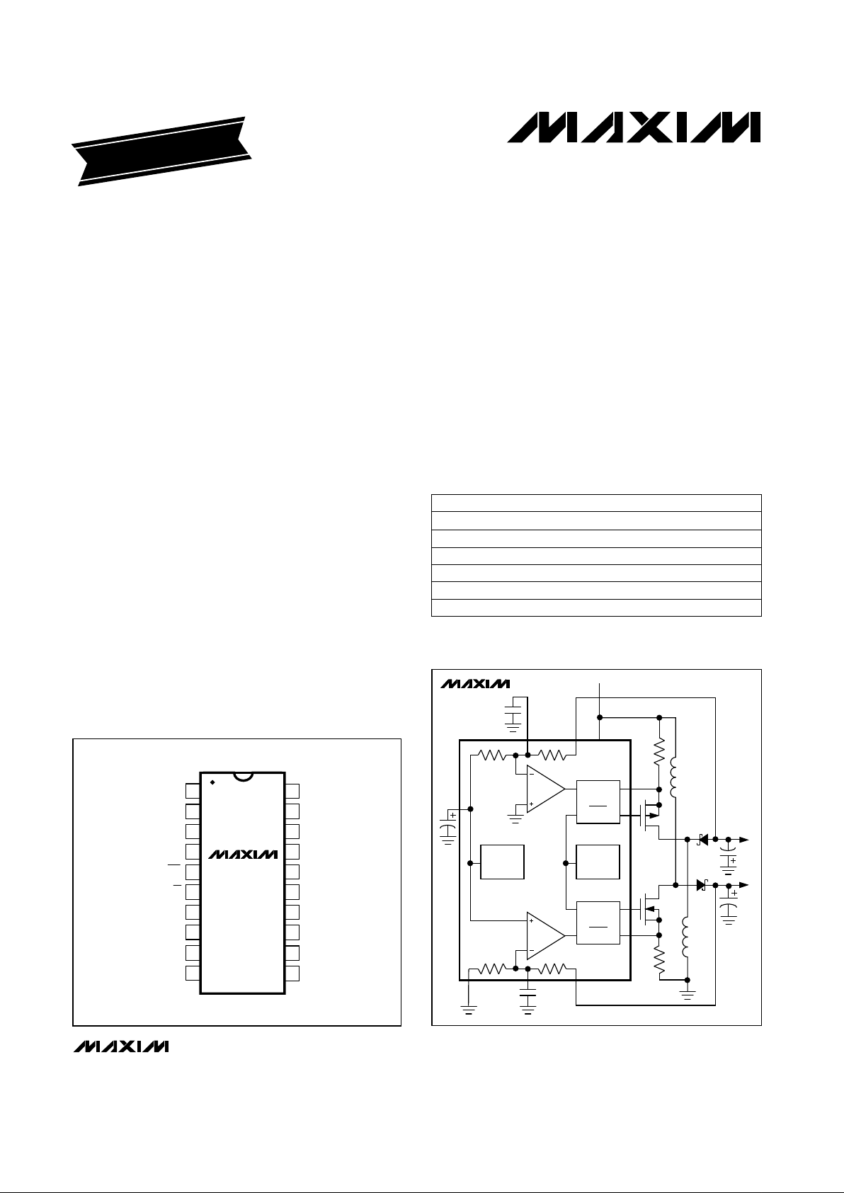
MAX742
P
R
+5V
INPUT
S
-SENSE
-DRIVE
PWM
N
R
S
+SENSE
+DRIVE
-VO
+VO
PWM
OSC
+2.0V
VREF
CC+
CC-
__________Simplified Block Diagram
20
19
18
17
16
15
14
13
1
2
3
4
5
6
7
8
CSH+
CSL+
GND
EXT+
AV
AGND
CC+
FB+
TOP VIEW
PUMP
PDRV
EXTV+
SS
VREF
12/15
100/200
12
11
9
10
CSHCSL-
FB-
CC-
DIP/SO
MAX742
__________________Pin Configuration
19-3105; Rev 2; 8/96
PART
MAX742CPP
MAX742CWP
MAX742C/D 0°C to +70°C
0°C to +70°C
0°C to +70°C
TEMP. RANGE PIN-PACKAGE
20 Plastic DIP
20 Wide SO
Dice*
EVALUATION KIT MANUAL
FOLLOWS DATA SHEET
MAX742EWP
MAX742MJP -55°C to +125°C
-40°C to +85°C 20 Wide SO
20 CERDIP
MAX742EPP -40°C to +85°C 20 Plastic DIP
______________Ordering Information
* Contact factory for dice specifications
For free samples & the latest literature: http://www.maxim-ic.com, or phone 1-800-998-8800
MAX742
Switch-Mode Regulator with
+5V to ±12V or ±15V Dual Output
2 _______________________________________________________________________________________
ABSOLUTE MAXIMUM RATINGS
ELECTRICAL CHARACTERISTICS
(Circuit of Figure 2, +4.5V < V+ < +5.5V.)
Stresses beyond those listed under “Absolute Maximum Ratings” may cause permanent damage to the device. These are stress ratings only, and functional
operation of the device at these or any other conditions beyond those indicated in the operational sections of the specifications is not implied. Exposure to
absolute maximum rating conditions for extended periods may affect device reliability.
V+, AV+ to AGND, GND.........................................-0.3V to +12V
PDRV to V+.............................................................+0.3V to -14V
FB+, FB- to GND..................................................................±25V
Input Voltage to GND
(CC+, CC-, CSH+, CSL+, CSH-, CSL-,
SS, 100/200
, 12/15)..................................-0.3V to (V+ + 0.3V)
Output Voltage to GND
(EXT+, PUMP) ..........................................-0.3V to (V+ + 0.3V)
EXT- to PDRV................................................-0.3V to (V+ + 0.3V)
Continuous Power Dissipation (any package)
up to +70°C.....................................................................500mW
derate above +70°C by ..........................................100mW/°C
Operating Temperature Ranges
MAX742C_ _ .......................................................0°C to +70°C
MAX742E_ _ ....................................................-40°C to +85°C
MAX742MJP ..................................................-55°C to +125°C
Storage Temperature Range.............................-65°C to +150°C
Lead Temperature (soldering, 10sec).............................+300°C
0mA < IL< 100mA,
12/15 = 0V
CONDITIONS
14.40 15.60
V
14.55 15.45
Output Voltage, ±15V Mode
(Notes 1, 2)
UNITSMIN TYP MAXSYMBOLPARAMETER
TA= +25°C
TA= T
MIN
to T
MAX
TA= +25°C
TA= T
MIN
to T
MAX
0mA < IL< 125mA,
12/15 = V+
11.52 12.48
V
11.64 12.36
Output Voltage, ±12V Mode
(Notes 1, 2)
No EXT- or PUMP load,
FB+ = FB- = open circuit
I
LOAD
= 0mA to 100mA
V+ = 4.5V to 5.5V, PDRV from PUMP
CSL+ = 0V, FB+ = open circuit
EXT+ or EXT-
100/200 = V+
100/200 = 0V
CSH- = V+, FB- = open circuit
CONDITIONS
mV150 225 300
Negative Current-Limit Threshold
(CSH- to CSL-)
mA
3
No-Load Supply Current
mV30 100
%/%0.01 0.05Line Regulation
Load Regulation (Note 2)
mV150 225 300
Positive Current-Limit Threshold
(CSH+ to CSL+)
%85 90Duty-Cycle Limit (Note 3)
kHzf
OSC
/2PUMP Frequency
kHz
75 100 125
V3.8 4.2UVLOUndervoltage Lockout
V0.2Undervoltage Lockout Hysteresis
V2.0Reference Output Voltage
170 200 230
f
OSC
Oscillator Frequency
UNITSMIN TYP MAXSYMBOLPARAMETER
V+ = 5V
ELECTRICAL CHARACTERISTICS
(Circuit of Figure 2, V+ = 5V, 100/200 = 12/15 = 0V; TA= T
MIN
to T
MAX
, unless otherwise noted.)
10V+ = 10V
MAX742
Switch-Mode Regulator with
+5V to ±12V or ±15V Dual Output
_______________________________________________________________________________________ 3
Note 1: Devices are 100% tested to these limits under 0mA to 100mA and to 125mA conditions using automatic test equipment.
The ability to drive loads up to 1A is guaranteed by the current-limit threshold, output swing, and the output current
source/sink tests. See Figures 2 and 3.
Note 2: Actual load capability of the circuit of Figure 2 is ±200mA in ±15V mode and ±250mA in ±12V mode. Load regulation is
tested at lower limits due to test equipment limitations.
Note 3: Guaranteed by design.
Note 4: Measured at Point A, circuit of Figure 2, with PDRV disconnected.
ELECTRICAL CHARACTERISTICS (continued)
(Circuit of Figure 2, V+ = 5V, 100/200 = 12/15 = 0V; TA= T
MIN
to T
MAX
, unless otherwise noted.)
EXT+, EXT-, IL= -1mA, V+ = 4.5V, PDRV= -3V
EXT+, EXT-, IL= 1mA, V+ = 4.5V, PDRV= -3V
V+ = 3.8V, SS = 2V
CC+, CC-
V+ = 4.5V, PDRV = -3V,
TA= +25°C
V+ = 4.5V, IL= -5mA, TA= +25°C
SS = 0V
CONDITIONS
mA-2 -0.5Soft-Start Sink Current
µA37Soft-Start Source Current
V-2.8V
OL
V4.3V
OH
Output Voltage High
Output Voltage Low
°C190Thermal-Shutdown Threshold
kΩ10Compensation Pin Impedance
mA
100 200
Output Sink Current
200 350
V-3PUMP Output Voltage (Note 4)
UNITSMIN TYP MAXSYMBOLPARAMETER
EXT+ = 4.5V
EXT- = 4.5V
EXT+ = 0V
V+ = 4.5V, PDRV = -3V,
TA= +25°C
EXT- = -3V
mA
-200 -100
Output Source Current
-350 -200
EXT+, C
LOAD
= 2nF
ns
70
Output Rise/Fall Time
100EXT-, C
LOAD
= 4nF, PDRV = -3V
MAX742
Switch-Mode Regulator with
+5V to ±12V or ±15V Dual Output
4 _______________________________________________________________________________________
__________________________________________Typical Operating Characteristics
(Circuit of Figure 2, V+ = 5V, TA = +25°C, unless otherwise noted.)
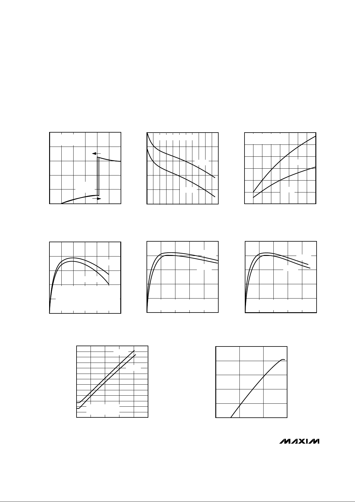
25
06
UNDERVOLTAGE LOCKOUT HYSTERESIS
5
10
20
MAX742 -1
SUPPLY VOLTAGE (V)
QUIESCENT SUPPLY CURRENT (mA)
15
4
23 51
±15V MODE,
200kHz MODE
LOCKOUT
ENABLED
-4.5
0
CHARGE-PUMP LOAD REGULATION
-2.5
-5.0
-3.0
-4.0
MAX742 -2
CHARGE-PUMP LOAD CURRENT (mA)
CHARGE-PUMP OUTPUT VOLTAGE (V)
-3.5
4
23 75 6 10 891
MEASURED AT POINT A
V+ = 5V
V+ = 4.5V
5
0
PDRV CURRENT vs. C
EXT-
1
6
2
4
MAX742 -3
CAPACITANCE AT EXT- (nF)
PDRV CURRENT (mA)
3
4
231
PDRV FORCED TO -4V
PUMP DISCONNECTED
200kHz
100kHz
50
0
EFFICIENCY vs. LOAD CURRENT,
22W CIRCUIT, ±15V MODE
60
70
90
MAX742 -4
LOAD CURRENT (mA)
EFFICIENCY (%)
80
±800
±400 ±600 ±1000±200
100kHz
200kHz
CIRCUIT OF FIGURE 3,
INDUCTORS = GOWANDA 121-AT2502
(MPP CORE),
Q2 = TWO IRF9Z30 IN PARALLEL
±15V MODE
0
PEAK INDUCTOR CURRENT vs.
LOAD CURRENT
100
200
400
MAX742 -7
LOAD CURRENT (mA)
PEAK INDUCTOR CURRENT (mA)
300
500
700
600
800
1000
900
1100
1200
200
100 15050
100kHz
200kHz
MEASURED AT LX-,
±15V MODE
50
0
EFFICIENCY vs. LOAD CURRENT,
6W CIRCUIT, ±15V MODE
60
70
90
MAX742 -5
LOAD CURRENT (mA)
EFFICIENCY (%)
80
±200
±100 ±150 ±250±50
100kHz
200kHz
INDUCTORS = GOWANDA 050-AT1003
(MPP CORE)
50
0
EFFICIENCY vs. LOAD CURRENT,
6W CIRCUIT, ±12V MODE
60
70
90
MAX742 -6
LOAD CURRENT (mA)
EFFICIENCY (%)
80
±300
±150 ±225±75
100kHz
200kHz
INDUCTORS = GOWANDA 050-AT1003
(MPP CORE)
0
CURRENT-LIMIT THRESHOLD vs.
SOFT-START VOLTAGE
50
100
200
MAX742 -8
SOFT-START VOLTAGE (V)
CURRENT-LIMIT THRESHOLD (mV)
150
3
12

MAX742
Switch-Mode Regulator with
+5V to ±12V or ±15V Dual Output
_______________________________________________________________________________________ 5
A = GATE DRIVE, 5V/div
B = SWITCH VOLTAGE, 10V/div
C = SWITCH CURRENT, 0.2A/div
SWITCHING WAVEFORMS,
INVERTING SECTION
A
B
C
2µs/div
_____________________________Typical Operating Characteristics (continued)
(Circuit of Figure 2, I
LOAD
= 100mA, unless otherwise noted.)
A = GATE DRIVE, 5V/div
B = SWITCH VOLTAGE, 10V/div
C = SWITCH CURRENT, 0.2A/div
SWITCHING WAVEFORMS,
STEP-UP SECTION
A
B
C
2µs/div
A = NOISE WITH i FILTER, 1mV/div
B = NOISE WITHOUT FILTER, 20mV/div
MEASURED AT -V
OUT
V+ = 5V
BW = 5MHz
OUTPUT-VOLTAGE NOISE,
FILTERED AND UNFILTERED
A
B
2µs/div
A = +VO, 20mV/div
B = -VO, 50mV/div
LOAD-TRANSIENT RESPONSE
A
B
200µs/div

MAX742
Switch-Mode Regulator with
+5V to ±12V or ±15V Dual Output
6 _______________________________________________________________________________________
______________________________________________________________Pin Description
Inverting Compensation CapacitorCC-9
Inverting Section Feedback InputFB-10
Current-Sense Low (inverting section)CSL-11
Current-Sense High (inverting section)CSH-12
Supply Voltage Input (+5V)V+13
Selects oscillator frequency. Ground for 200kHz, or tie to V+ for 100kHz.100/2005
Selects V
OUT
. Ground for ±15V, or tie to V+ for ±12V.12/156
Reference Voltage Output (+2.00V). Force to GND or V+ to disable chip.VREF7
Soft-Start Timing Capacitor (sources 5µA)SS8
Analog Supply Voltage Input (+5V)AV+4
Analog GroundAGND3
PIN
Step-Up Compensation CapacitorCC+2
Step-Up Feedback InputFB+1
FUNCTIONNAME
Charge-Pump Driver—clock output at 1/2 oscillator frequency.PUMP16
Push-Pull Output—drives external logic-level N-channel MOSFET.EXT+17
High-Current GroundGND18
Current-Sense Low (step-up section)CSL+19
Current-Sense High (step-up section)CSH+20
Push-Pull Output—drives external P-channel MOSFET.EXT-14
Voltage Input—negative supply for P-channel MOSFET driver.PDRV15
________________Operating Principle
Each current-mode controller consists of a summing
amplifier that adds three signals: the current waveform
from the power switch FET, an output-voltage error signal, and a ramp signal for AC compensation generated
by the oscillator. The output of the summing amplifier
resets a flip-flop, which in turn activates the power FET
driver stage (Figure 1).
Both external transistor switches are synchronized to
the oscillator and turn on simultaneously when the flipflop is set. The switches turn off individually when their
source currents reach a trip threshold determined by
the output-voltage error signal. This creates a dutycycle modulated pulse train at the oscillator frequency,
where the on time is proportional to both the outputvoltage error signal and the peak inductor current. Low
peak currents or high output-voltage error signals result
in a high duty cycle (up to 90% maximum).
AC stability is enhanced by the internal ramp signal
applied to the error amplifier. This scheme eliminates
regenerative “staircasing” of the inductor current, which
is otherwise a problem when in continuous current
mode with greater than 50% duty cycle.

_______________Detailed Description
100kHz/200kHz Oscillator
The MAX742 oscillator frequency is generated without
external components and can be set at 100kHz or
200kHz by pin strapping. Operating the device at
100kHz results in lower supply current and improved
efficiency, particularly with light loads. However, component stresses increase and noise becomes more difficult to filter. For a given inductor value, the lower
operating frequency results in slightly higher peak currents in the inductor and switch transistor (see
Typical
Operating Characteristics
, Peak Inductor Current vs.
Load Current graph). When the lower frequency is used
in conjunction with an LC-type output filter (optional
components in Figure 2), larger component values are
required for equivalent filtering.
Charge-Pump Voltage Inverter
The charge-pump (PUMP) output is a rail-to-rail square
wave at half the oscillator frequency. The square wave
drives an external diode-capacitor circuit to generate a
negative DC voltage (Point A in Figure 2), which in turn
biases the inverting-output drive stage via PDRV. The
charge pump thus increases the gate-source voltage
applied to the external P-channel FET. The low onresistance resulting from increased gate drive ensures
high efficiency and guarantees start-up under heavy
loads. If a -5V to -8V supply is already available, it can
be tied directly to PDRV and all of the charge-pump
components removed. For input voltages greater than
8V, ground PDRV to prevent overvoltage. Observe
PDRV absolute maximum ratings.
MAX742
Switch-Mode Regulator with
+5V to ±12V or ±15V Dual Output
_______________________________________________________________________________________ 7
MAX742
PULSE
SQUARE
RAMP
OSC
12/15
SELECT
VREF
SOFT-START
AND THERMAL
SHUTDOWN
S
RQ
S
TO V+
RQ
∑
∑
AGND
VREF
12/15
CC-FB-
CC+FB+
CSH+
CSL+
V+
EXT+
GND
SS
PUMP
EXTPDRV
CSH-
CSL-
AV+100/200
Figure1. MAX742 Detailed Block Diagram

MAX742
Switch-Mode Regulator with
+5V to ±12V or ±15V Dual Output
8 _______________________________________________________________________________________
MAX742
Q2
Q1
CSH+
VIN
4.5V to 6V*
CSL+
1
J1
C2
3.3nF
+VO
OPTIONAL
D1
L3
25µH
L1
100µH
C8
150µF
C6
D4
D3
C9
150µF
C14
2.2µF
GND
EXT+
PUMP
PDRV
EXT-
V+
CSH-
CSL-
C7
1µF
C13
0.1µF
DISC CERAMIC
C1
0.1µF
NOTES:
Q1 = Motorola MTP15N05L
Q2 = Motorola MTP12P05
L1, L2 = MAXL001
C8–C12 = MAXC001
D1, D2 = 1N5817
D3, D4 = Fuji ERA82-004 or 1N5817
R2, R3 = RCD RSF 1A Metal Film ±3%
L3, L4 = Wilco MFB 250
R3
0.1Ω
C10
150µF
C3
10µF
R1
100Ω
C4
C5
3.3nF
L2
100µH
-VO
POINT
A
OPTIONAL
D2
L4
25µH
C11
150µF
C12
150µF
C15
2.2µF
1µF
FB+
CC+
AGND
AV+
100/200
12/15
VREF
* FOR HIGHER INPUT VOLTAGE, SEE
SUPPLY-VOLTAGE RANGE
SECTION.
SS
CC-
FB-
R2
0.16Ω
Figure 2. Standard 6W Application Circuit

MAX742
Switch-Mode Regulator with
+5V to ±12V or ±15V Dual Output
_______________________________________________________________________________________ 9
MAX742
Q2
Q1
CSH+
VIN
4.5V to 6V*
CSL+
1
J1
C2
6.8nF
+VO
D1
1N5820
L1
25µH
R2
0.02Ω
C8
1000µF
C6
D4
1N914
D3
1N914
C9
1000µF
GND
EXT+
PUMP
PDRV
EXT-
V+
CSH-
CSL-
C7
1µF
C14
0.1µF
DISC CERAMIC
C1
0.1µF
NOTES:
Q1 = Motorola MTP25N06L
Q2 = International Rectifier IRF9Z30
L1, L2 = Gowanda 121AT2502VC
R2, R3 = KRL LB4-1 ±3%
C8–C13 = Nichicon PL Series (25V or 35V)
R3
0.02Ω
C10
1000µF
10V
C3
10µF
R1
100Ω
C4
2.2µF
C5
6.8nF
L2
25µH
-VO
D2
1N5820
C11
1000µF
C12
1000µF
1µF
FB+
CC+
AGND
AV+
100/200
12/15
VREF
* FOR HIGHER INPUT VOLTAGE, SEE
SUPPLY-VOLTAGE RANGE
SECTION.
SS
CC-
FB-
C13
330µF
Figure 3. High-Power 22W Application Circuit

MAX742
Switch-Mode Regulator with
+5V to ±12V or ±15V Dual Output
10 ______________________________________________________________________________________
Supply-Voltage Range
Although designed for operation from a +5V logic
supply, the MAX742 works well from 4.2V (the upper
limit of the undervoltage lockout threshold) to +10V
(absolute maximum rating plus a safety margin). The
upper limit can be further increased by limiting the
voltage at V+ with a zener shunt or series regulator.
To ensure AC stability, the inductor value should be
scaled linearly with the nominal input voltage. For
example, if Figure 3’s application circuit is powered
from a nominal 9V source, the inductor value should be
increased to 40µH or 50µH. At high input voltages
(>8V), the charge pump can cause overvoltage at
PDRV. If the input can exceed 8V, ground PDRV and
remove the capacitors and diodes associated with the
charge pump.
In-Circuit Testing for
Guaranteed Performance
Figure 2’s circuit has been tested at all extremes of line,
load, and temperature. Refer to the
Electrical
Characteristics
table for guaranteed in-circuit specifications. Successful use of this circuit requires no component calculations.
Soft-Start
A capacitor connected between Soft-Start (SS) and
ground limits surge currents at power-up. As shown in
the
Typical Operating Characteristics
, the peak switch
current limit is a function of the voltage at SS. SS is
internally connected to a 5µA current source and is
diode-clamped to 2.6V (Figure 8). Soft-start timing is
therefore set by the SS capacitor value. As the SS voltage ramps up, peak inductor currents rise until they
reach normal operating levels. Typical values for the SS
capacitor, when it is required at all, are in the range of
1µF to 10µF.
Fault Conditions Enabling SS Reset
In addition to power-up, the soft-start function is enabled
by a variety of fault conditions. Any of the following conditions will cause an internal pull-down transistor to discharge the SS capacitor, triggering a soft-start cycle:
Undervoltage lockout
Thermal shutdown
VREF shorted to ground or supply
VREF losing regulation
__________________Design Procedure
Inductor Value
An exact inductor value isn’t critical. The inductor value
can be varied in order to make tradeoffs between
noise, efficiency, and component sizes. Higher inductor
values result in continuous-conduction operation, which
maximizes efficiency and minimizes noise. Physically
smallest inductors (where E = 1/2 LI2is minimum) are
realized when operating at the crossover point between
continuous and discontinuous modes. Lowering the
inductor value further still results in discontinuous current even at full load, which minimizes the output
capacitor size required for AC stability by eliminating
the right-half-plane zero found in boost and inverting
topologies. Ideal current-mode slope compensation
where m = 2 x V/L is achieved if L (Henries) = R
SENSE
(Ω) x 0.001, but again the exact value isn’t critical and
the inductor value can be adjusted freely to improve
AC performance. The following equations are given for
continuous-conduction operation since the MAX742 is
mainly intended for low-noise analog power supplies.
See Appendix A in Maxim’s
Battery Management and
DC-DC Converter Circuit Collection
for crossover point
and discontinuous-mode equations.
Boost (positive) output:
(VIN- VSW)2(V
OUT
+ VD- VIN)
L = ———————————————
(V
OUT
+ VD)2(I
LOAD
)(F)(LIR)
Inverting (negative) output:
(V
IN
- VSW)
2
L = —————————————
(V
OUT
+ VD)(I
LOAD
)(F)(LIR)
MAX742
N
8
EXTERNAL
SS
CAPACITOR
5µA
+5V
TO CURRENT–
LIMIT COMPARATOR
FAULT
SS
+2V
REFERENCE
Figure 4. Soft-Start Equivalent Circuit

MAX742
Switch-Mode Regulator with
+5V to ±12V or ±15V Dual Output
______________________________________________________________________________________ 11
where:
VSWis the voltage drop across the the switch transistor
and current-sense resistor in the on state (0.3V typ).
VDis the rectifier forward voltage drop (0.4V typ).
LIR is the ratio of peak-to-peak ripple current to DC
offset current in the inductor (0.5 typ).
Current-Sense Resistor Value
The current-sense resistor values are calculated according to the worst-case-low current-limit threshold voltage
from the
Electrical Characteristics
table and the peak
inductor current. The peak inductor current calculations
that follow are also useful for sizing the switches and
specifying the inductor current saturation ratings.
150mV
R
SENSE
= ————
I
PEAK
I
LOAD(VOUT
+ VD)
+I
PEAK
(boost) = ————————— +
VIN- V
SW
(VIN- VSW) (V
OUT
+ VD- VIN)
—————————————
(2)(F)(L)(V
OUT
+ VD)
I
LOAD(VOUT
+ VD+ VIN)
+I
PEAK
(inverting) = ———————————— +
VIN- V
SW
(VIN- VSW) (V
OUT
+ VD+ VIN)
—————————————
(2)(F)(L) (V
OUT
+ VD)
Filter Capacitor Value
The output filter capacitor values are generally determined by the effective series resistance (ESR) and voltage rating requirements rather than actual capacitance
requirements for loop stability. In other words, the
capacitor that meets the ESR requirement for noise purposes nearly always has much more output capacitance than is required for AC stability. Output voltage
noise is dominated by ESR and can be roughly calculated by an Ohm’s Law equation:
V
NOISE
(peak-to-peak) = I
PEAK
x R
ESR
where V
NOISE
is typically 0.15V.
Ensure the output capacitors selected meet the following minimum capacitance requirements:
Minimum CF = 60µF per output or the following, whichever is greater:
CF = 0.015/R
LOAD
(in Farads, ±15V mode)
CF = 0.01/R
LOAD
(in Farads, ±12V mode)
Compensation Capacitor (CC) Value
The compensation capacitors (CC+ and CC-) cancel
the zero introduced by the output filter capacitors’ ESR,
improving phase margin, and AC stability. The compensation poles set by CC+ and CC- should be set to
match the ESR zero frequencies of the output filter
capacitors according to the following:
R
ESR
x CF
CC (in Farads) = —————— (use 1000pF minimum)
10kΩ
Standard 6W Application
The 6W supply (Figure 2) generates ±200mA at ±15V,
or ±250mA at ±12V. Output capability is increased to
10W or more by heatsinking the power FETs, using
cores with higher current capability (such as Gowanda
#050AT1003), and using higher filter capacitance.
Ferrite and MPP inductor cores optimize efficiency and
size. Iron-power toroids designed for high frequencies
are economical, but larger.
Ripple is directly proportional to filter capacitor equivalent series resistance (ESR). In addition, about 250mV
transient noise occurs at the LX switch transitions. A
very short scope probe ground lead or a shielded
enclosure is need for making accurate measurements
of transient noise. Extra filtering, as shown in Figure 2,
reduces both noise components.
High-Power 22W Application
The 22W application circuit (Figure 3) generates ±15V
at ±750mA or ±12V at ±950mA. Noninductive wirewound resistors with Kelvin current-sensing connections replace the metal-film resistors of the previous
(6W) circuit. Gate drive for the P-channel FET is bootstrapped from the negative supply via diode D6. The
2.7V zener (D5) is required in 15V mode to prevent
overvoltage. The charge pump (D3, D4, and C6) may
not be necessary if the circuit is lightly loaded
(<100mA) on start-up. AIE part #415-0963 is a ferrite
pot-core inductor that can be used in place of a smaller, more expensive moly-permalloy toroid inductor (L1,
L2). Higher efficiencies can be achieved by adding
extra MOSFETs in parallel. Load levels above 10W
make it necessary to add heatsinks, especially to the Pchannel FET.

MAX742
Switch-Mode Regulator with
+5V to ±12V or ±15V Dual Output
12 ______________________________________________________________________________________
Table 1. Trouble-Shooting Chart
___________________Chip Topography
GND
EXT+
V+
EXT-
AV+
PUMP
PDRV
12/15
100/200
VREF
AGND
CC+ FB+
CSH+ CSL+
CSH-
CSL- CC-
SS
FB-
0.135"
(3.45mm)
0.080"
(2.03mm)
TRANSISTOR COUNT: 375
SUBSTRATE CONNECTED TO V+
SYMPTOM CORRECTION
Output is unloaded. Apply ±30mA or
greater load to observe waveform.
No Switching.
±VO are correct,
but no waveform is
seen at LX+ or LX-.
A. Check connections. VREF should be +2V.
B. When input voltage is less than +4.2V,
undervoltage lockout is enabled.
No Output. +VO
= 5V or less. -VO
= 0V.
A. Inductor saturation: Peak currents
exceed coil ratings.
B. MOSFET on-resistance too high.
C. Switching losses: Diode is slow or has high
forward voltage. Inductor has high DC resis-
tance. Excess capacitance at LX nodes.
D. Inductor core losses: Hysteresis losses
cause self-heating in some core materials.
E. Loop instability: See Unstable Output
above.
Poor Efficiency.
Supply current is
high. Output will
not drive heavy
loads.
A. Input overvoltage: Never apply more
than +12V.
B. FB+ or FB- disconnected or shorted. This
causes runaway and output overvoltage.
C. CC+ or CC- shorted.
D. Output filter capacitor disconnected.
Self-Destruction.
Transistors or IC
die on power-up.
A. Ground noise: Probe ground is picking up
switching EMI. Reduce probe ground lead
length (use probe tip shield) or put circuit
in shielded enclosure.
B. Poor HF response: Add ceramic or
tantalum capacitors in parallel with output
filter capacitors.
Noisy Output.
Switching is
steady, but large
inductive spikes
are seen at the
outputs.
Loop stability problem.
A. CC+ or CC- disconnected.
B. EMI: Move inductor away from IC or use
shielded inductors. Keep noise sources
away from CC- and CC+.
C. Grounding: Tie AGND directly to the filter
capacitor ground lead. Ensure that cur-
rent spikes from GND do not cause noise
at AGND or compensation capacitor or
reference bypass ground leads. Use wide
PC traces or a ground plane.
D. Bypass: Tie 10µF or larger between AGND
and VREF. Use 150µF to bypass the input
right at AV+. If there is high source resis-
tance, 1000µF or more may be required.
E. Current limiting: Reduce load currents.
Ensure that inductors are not saturating.
F. Slope compensation: Inductor value not
matched to sense resistor.
Unstable Output.
Noise or jitter on
output ripple
waveform. Scope
may not trigger
correctly.
 Loading...