MAXIM MAX7426, MAX7427 Technical data

现货库存、技术资料、百科信息、热点资讯,精彩尽在鼎好!
General Description
The MAX7426/MAX7427 5th-order, lowpass, elliptic,
switched-capacitor filters (SCFs) operate from a single
+5V (MAX7426) or +3V (MAX7427) supply. The devices
draw only 0.8mA of supply current and allow corner frequencies from 1Hz to 12kHz, making them ideal for
low-power post-DAC filtering and anti-aliasing applications. They can be put into a low-power mode, reducing
supply current to 0.2µA.
Two clocking options are available: self-clocking (through
the use of an external capacitor) or external clocking for
tighter cutoff-frequency control. An offset-adjust pin
allows for adjustment of the DC output level.
The MAX7426/MAX7427 deliver 37dB of stopband
rejection and a sharp rolloff with a transition ratio of
1.25. Their fixed response limits the design task to
selecting a clock frequency.
Applications
ADC Anti-Aliasing CT2 Base Stations
Post-DAC Filtering Speech Processing
Features
♦ 5th-Order, Elliptic Lowpass Filters
♦ Low Noise and Distortion: -80dB THD + Noise
♦ Clock-Tunable Corner Frequency (1Hz to 12kHz)
♦ Single-Supply Operation
+5V (MAX7426)
+3V (MAX7427)
♦ Low Power
0.8mA (Operating Mode)
0.2µA (Shutdown Mode)
♦ Available in 8-Pin µMAX/PDIP Packages
♦ Low Output Offset: ±4mV
MAX7426/MAX7427
5th-Order, Lowpass, Elliptic,
Switched-Capacitor Filters
________________________________________________________________ Maxim Integrated Products 1
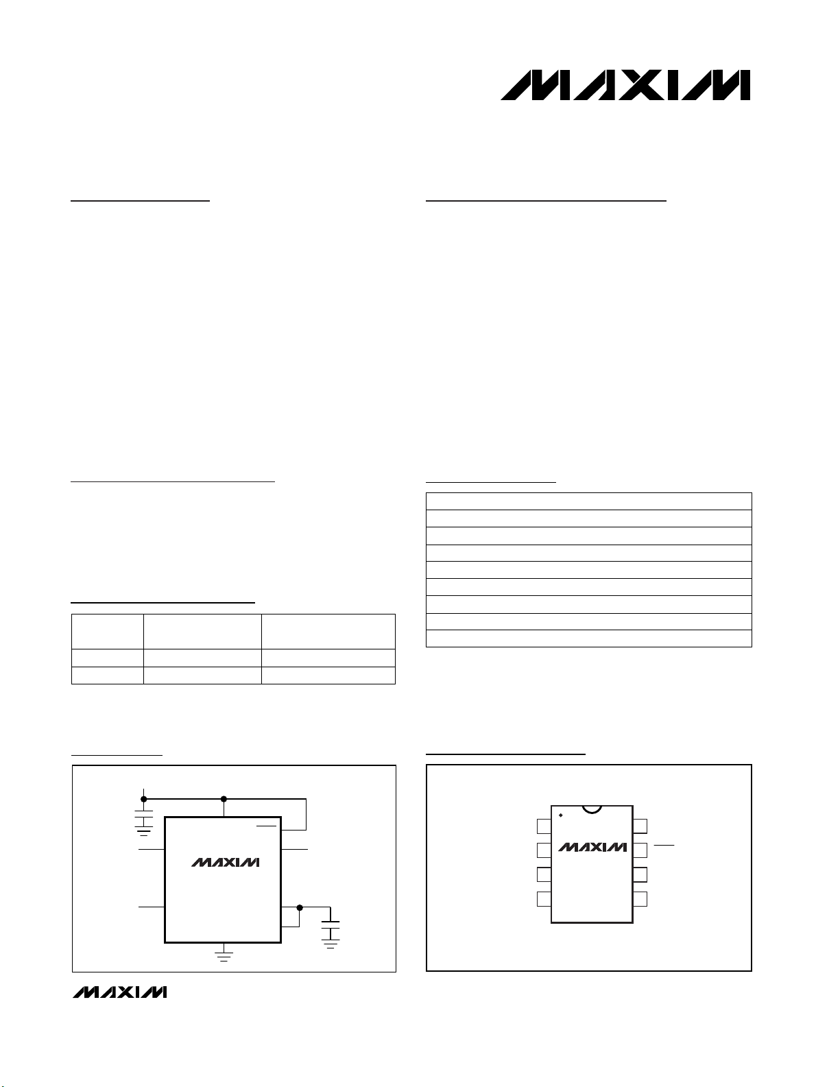
Typical Operating Circuit
19-1710; Rev 0; 4/00
Pin Configuration
Ordering Information
PART
MAX7426CUA
MAX7426CPA
MAX7426EUA -40°C to +85°C
0°C to +70°C
0°C to +70°C
TEMP. RANGE PIN-PACKAGE
8 µMAX
8 Plastic DIP
8 µMAX
MAX7426EPA -40°C to +85°C 8 Plastic DIP
PART
TRANSITION RATIO
OPERATING
VOLTAGE (V)
MAX7426 r = 1.25 +5
Selector Guide
MAX7427 r = 1.25 +3
MAX7427CUA
MAX7427CPA
MAX7427EUA -40°C to +85°C
0°C to +70°C
0°C to +70°C 8 µMAX
8 Plastic DIP
8 µMAX
MAX7427EPA -40°C to +85°C 8 Plastic DIP
For free samples and the latest literature, visit www.maxim-ic.com or phone 1-800-998-8800.
For small orders, phone 1-800-835-8769.
87CLK
MAX7426
MAX7427
µMAX/PDIP
SHDNIN
OS
6
OUTV
5
0.1µF
INPUT
CLOCK
V
SUPPLY
V
DD
SHDN
IN
MAX7426
MAX7427
CLK
GND
OUT
COM
OUTPUT
OS
0.1µF
TOP VIEW
COM
GND
1
2
3
4
DD

MAX7426/MAX7427
5th-Order, Lowpass, Elliptic,
Switched-Capacitor Filters
2 _______________________________________________________________________________________
ABSOLUTE MAXIMUM RATINGS
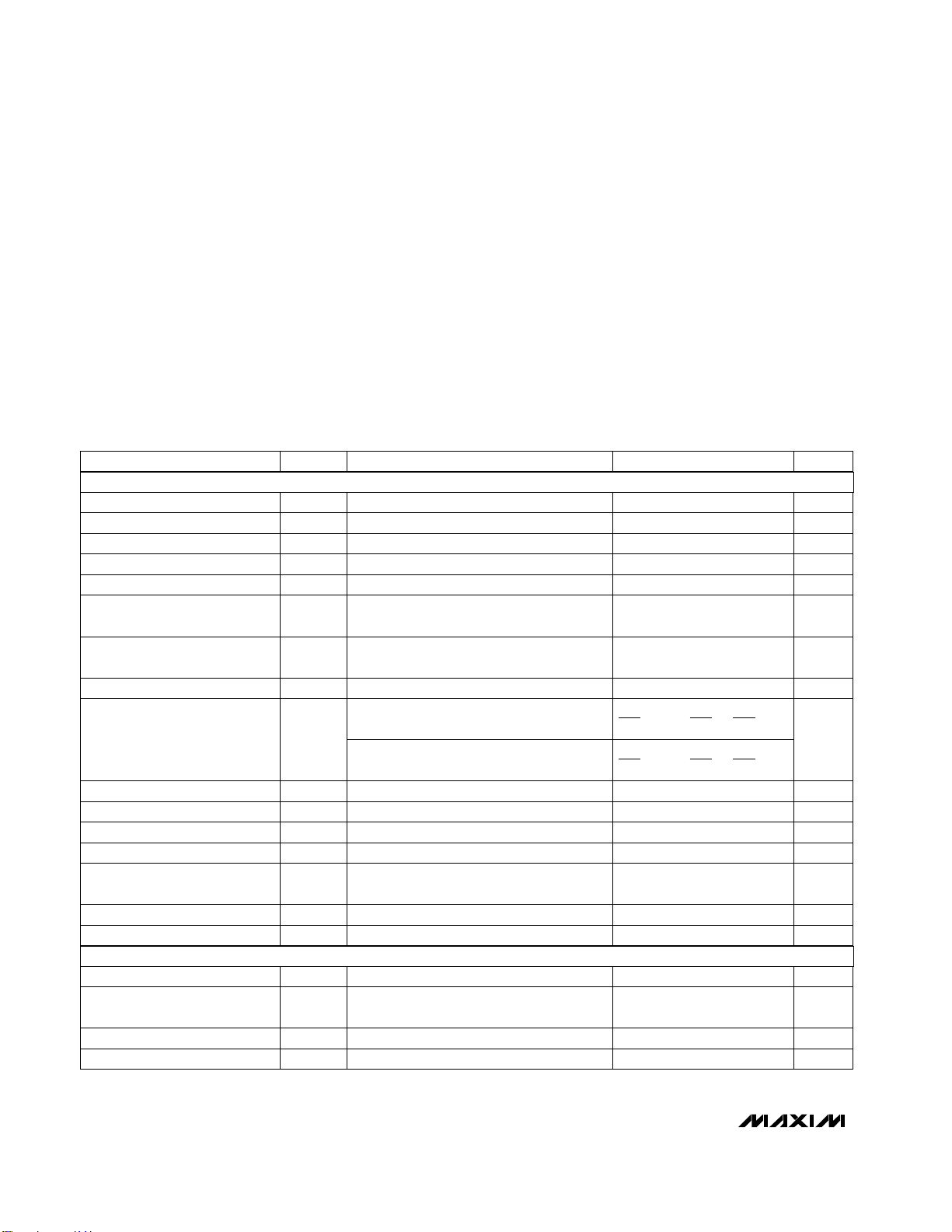
ELECTRICAL CHARACTERISTICS—MAX7426
(VDD= +5V, filter output measured at OUT, 10kΩ
|| 50pF load to GND at OUT, SHDN = V
DD
, OS = COM, 0.1µF from COM to GND,
f
CLK
= 100kHz, TA= T
MIN
to T
MAX
, unless otherwise noted. Typical values are at TA= +25°C.)
Stresses beyond those listed under “Absolute Maximum Ratings” may cause permanent damage to the device. These are stress ratings only, and functional
operation of the device at these or any other conditions beyond those indicated in the operational sections of the specifications is not implied. Exposure to
absolute maximum rating conditions for extended periods may affect device reliability.
VDDto GND..............................................................-0.3V to +6V
IN, OUT, COM, OS, CLK, SHDN ................-0.3V to (V
DD
+ 0.3V)
OUT Short-Circuit Duration.......................................................1s
Continuous Power Dissipation (T
A
= +70°C)
8-Pin µMAX (derate 4.1mW/°C above +70°C) .............330mW
8-Pin PDIP (derate 6.90mW/°C above +70°C).............552mW
Operating Temperature Ranges
MAX742 _C_A....................................................0°C to +70°C
MAX742 _E_A .................................................-40°C to +85°C
Storage Temperature Range .............................-65°C to +160°C
Lead Temperature (soldering, 10s) .................................+300°C
C
OSC
= 1000pF (Note 3)
VOS= 0 to V
DD
SHDN = GND, V
COM
= 0 to V
DD
(Note 1)
TA= +25°C
Input, COM externally driven
OS to OUT
Measured with respect to COM
fIN= 200Hz, VIN= 4Vp-p,
measurement bandwidth = 22kHz
VIN= V
COM
= V
DD
/ 2
V
COM
= V
DD
/ 2 (Note 2)
Output, COM internally driven
CONDITIONS
13.5 17.5 21.5f
OSC
Internal Oscillator Frequency
±0.2 ±10Input Leakage Current at OS
±0.2 ±10Input Leakage Current at COM
50 500C
L
10 1R
L
Resistive Output Load Drive
5Clock Feedthrough
90 130R
COM
Input Resistance at COM
±0.1V
OS
Input Voltage Range at OS
V
DD
- 0.2
V
DDVDD
+ 0.2
2 2 2
100:1f
CLK/fC
Clock-to-Corner Ratio
0.001 to 9f
C
Corner-Frequency Range
V
DD
- 0.5
V
DDVDD
+ 0.5
2 2 2
V
COM
COM Voltage Range
+1A
OS
Offset Voltage Gain
-81THD+N
Total Harmonic Distortion plus
Noise
10Clock-to-Corner Tempco
0.25 VDD- 0.25Output Voltage Range
±4 ±25V
OFFSET
Output Offset Voltage
0 0.2 0.4
DC Insertion Gain with Output
Offset Removed
MIN TYP MAXSYMBOLPARAMETER
0.5V
IL
Clock Input Low
4.5V
IH
Clock Input High
±8 ±12.5I
CLK
Clock Output Current
(internal oscillator mode)
V
V
µA
kHz
µA
µA
pF
kΩ
mVp-p
kΩ
V
V
V/V
dB
dB
mV
V
ppm/°C
kHz
UNITS
Maximum Capacitive Load
at OUT
FILTER
CLOCK

MAX7426/MAX7427
5th-Order, Lowpass, Elliptic,
Switched-Capacitor Filters
_______________________________________________________________________________________ 3
5th-Order, Lowpass, Elliptic,
Switched-Capacitor Filters
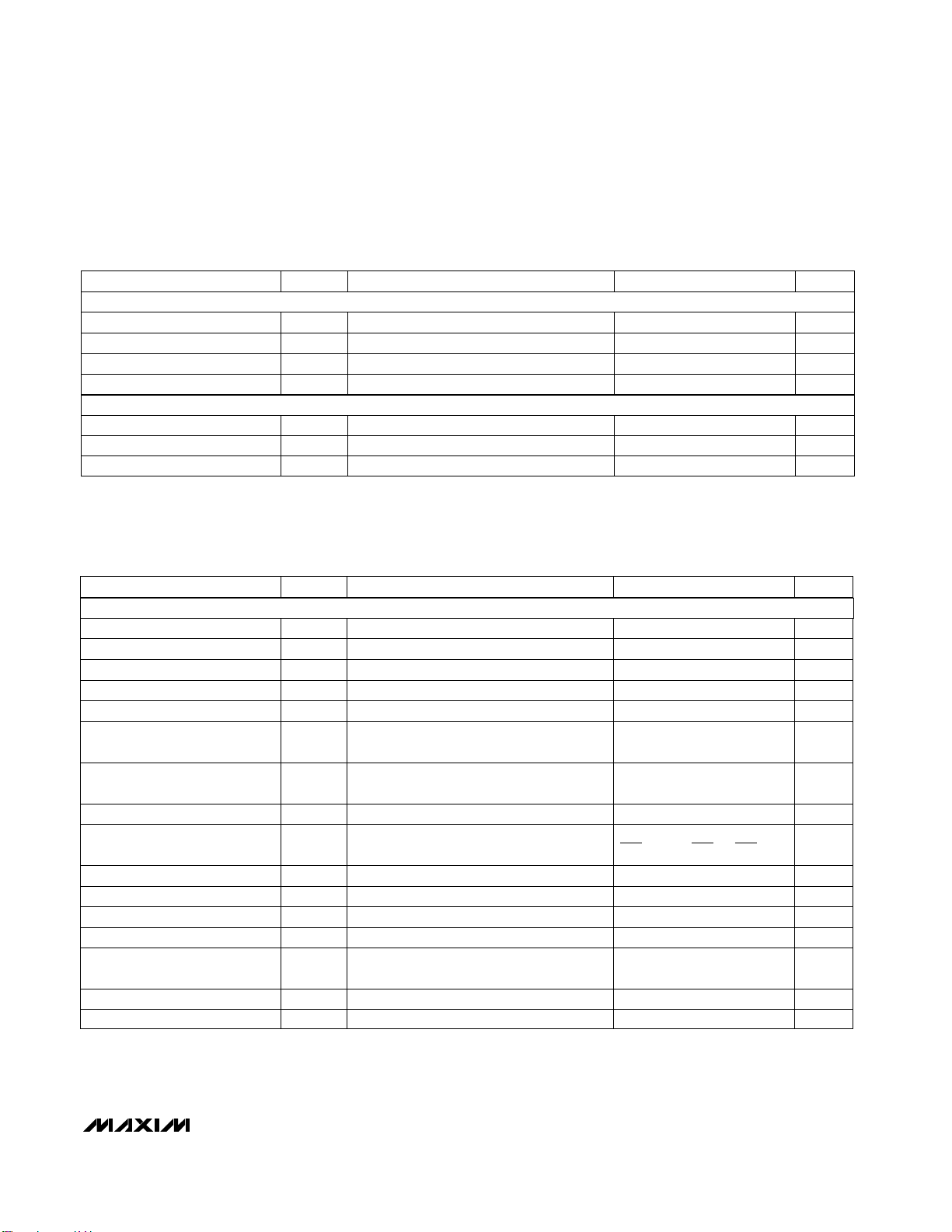
ELECTRICAL CHARACTERISTICS—MAX7426 (continued)
(VDD= +5V, filter output measured at OUT, 10kΩ
|| 50pF load to GND at OUT, SHDN = V
DD
, OS = COM, 0.1µF from COM to GND,
f
CLK
= 100kHz, TA= T
MIN
to T
MAX
, unless otherwise noted. Typical values are at TA= +25°C.)
ELECTRICAL CHARACTERISTICS—MAX7427
(VDD= +3V, filter output measured at OUT pin, 10kΩ || 50pF load to GND at OUT, SHDN = VDD, OS = COM, 0.1µF from COM to
GND, f
CLK
= 100kHz, TA= T
MIN
to T
MAX
, unless otherwise noted. Typical values are at TA= +25°C.)
CONDITIONS
MIN TYP MAXSYMBOLPARAMETER
Measured at DC
SHDN = GND
Operating mode, no load
0.5V
SDL
SHDN Input Low
4.5V
SDH
SHDN Input High
70PSRRPower-Supply Rejection Ratio
0.2 1I
SHDN
Shutdown Current
0.8 1.0Supply Current I
DD
4.5 5.5V
DD
Supply Voltage
V
V
dB
µA
mA
V
UNITS
SHDN Input Leakage Current
V
SHDN
= 0 to V
DD
±0.2 ±10 µA
V
OS
Input Voltage Range at OS
90 130R
COM
Input Resistance at COM kΩ
(Note 1)
TA= +25°C
Measured with respect to COM
OS to OUT
fIN= 200Hz, VIN= 2.5Vp-p,
measurement bandwidth = 22kHz
VIN= V
COM
= V
DD
/ 2
V
COM
= V
DD
/ 2 (Note 2)
CONDITIONS
50 500C
L
10 1R
L
Resistance Output Load Drive
3Clock Feedthrough
±0.1
V
DD
- 0.1
V
DDVDD
+ 0.1
2 2 2
V
COM
COM Voltage Range
100:1f
CLK
/
f
C
Clock-to-Corner Ratio
0.001 to 12f
C
Corner-Frequency Range
+1A
OS
Offset Voltage Gain
-79THD+N
Total Harmonic Distortion plus
Noise
10Clock-to-Corner Tempco
0.25 VDD- 0.25Output Voltage Range
±4 ±25V
OFFSET
Output Offset Voltage
0 0.2 0.4
DC Insertion Gain with Output
Offset Removed
MIN TYP MAXSYMBOLPARAMETER
pF
kΩ
mVp-p
V
V
V/V
dB
dB
mV
V
ppm/°C
kHz
UNITS
Maximum Capacitive Load
at OUT
Input Leakage Current at COM
SHDN = GND, V
COM
= 0 to V
DD
±0.2 ±10 µA
Input Leakage Current at OS VOS= 0 to V
DD
±0.2 ±10 µA
POWER REQUIREMENTS
SHUTDOWN
FILTER CHARACTERISTICS

MAX7426/MAX7427
5th-Order, Lowpass, Elliptic,
Switched-Capacitor Filters
4 _______________________________________________________________________________________
C
OSC
= 1000pF (Note 3)
CONDITIONS
13.5 17.5 21.5f
OSC
Internal Oscillator Frequency
MIN TYP MAXSYMBOLPARAMETER
Measured at DC
SHDN = GND
Operating mode, no load
V
CLK
= 0 or 3V
0.5V
SDL
SHDN Input Low
2.5V
SDH
SHDN Input High
70PSRRPower-Supply Rejection Ratio
0.2 1I
SHDN
Shutdown Current
0.75 1.0
2.7 3.6V
DD
Supply Voltage
0.5V
IL
Clock Input Low
2.5V
IH
Clock Input High
±7.5 ±12.5I
CLK
Clock Output Current
(internal oscillator mode)
V
V
dB
µA
V
V
V
µA
kHz
UNITS
SHDN Input Leakage Current
V
SHDN
= 0 to V
DD
±0.2 ±10 µA
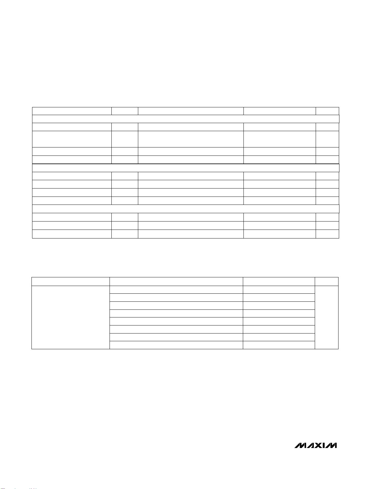
ELECTRICAL CHARACTERISTICS—MAX7427 (continued)
(VDD= +3V, filter output measured at OUT pin, 10kΩ
|| 50pF load to GND at OUT, SHDN = V
DD
, OS = COM, 0.1µF from COM to
GND, f
CLK
= 100kHz, TA= T
MIN
to T
MAX
, unless otherwise noted. Typical values are at TA= +25°C.)
ELLIPTIC FILTER CHARACTERISTICS (r = 1.25)
(VDD= +5V for MAX7426, VDD= +3V for MAX7427, filter output measured at OUT, 10kΩ || 50pF load to GND at OUT, SHDN = V
DD,
V
COM
= V
OS =VDD
/ 2, f
CLK
= 100kHz, TA = T
MIN
to T
MAX
, unless otherwise noted. Typical values are at TA= +25°C.) (Note 3)
Note 1: The maximum f
C
is defined as the clock frequency f
CLK
= 100 ✕fCat which the peak SINAD drops to 68dB with a sinu-
soidal input at 0.2f
C
.
Note 2: DC insertion gain is defined as ∆V
OUT
/ ∆VIN.
Note 3: f
OSC
(kHz) ≈ 17.5 ✕103/ C
OSC(COSC
in pF).
Note 4: The input frequencies, f
IN
, are selected at the peaks and troughs of the ideal elliptic frequency responses.
f
IN
= 0.68f
C
fIN= 0.38f
C
fIN= 3.25f
C
fIN= 1.43f
C
fIN= 1.25f
C
fIN= 0.87f
C
fIN= 0.97f
C
fIN= f
C
CONDITIONS
-0.4 0.2 0.4
dB
-0.4 -0.2 0.4
Insertion Gain
with DC Gain Error Removed
(Note 4)
-37.2 -35
-37.2 -35
-38.5 -34
-0.4 -0.2 0.4
-0.4 0.2 0.4
-0.7 -0.2 0.2
UNITSMIN TYP MAXPARAMETER
mAI
DD
Supply Current
CLOCK
POWER REQUIREMENTS
SHUTDOWN
 Loading...