

Page 1
General Description
The MAX7389/MAX7390 replace ceramic resonators,
crystals, and supervisory functions for microcontrollers
in 3.3V and 5V applications.
The MAX7389/MAX7390 provide a clock source, reset,
and watchdog functions. The watchdog timer is pin programmable and provides watchdog timeout values in
the 16ms to 2048ms range. The MAX7389 provides a
separate watchdog output that is used as a status indicator or to control safety-critical system elements.
The MAX7390 features a clock-speed select that
reduces the output frequency by half. This functionality
allows the microcontroller to operate at reduced power
and may be used to extend the time available to perform housekeeping tasks, such as writing data to flash
during a power failure.
The MAX7389/MAX7390 clock outputs are factory programmed to a frequency in the 1MHz to 16MHz range.
Four standard frequencies are available. Other frequencies are available upon request. The maximum operating
supply current is 5.5mA with a clock frequency of 12MHz.
Unlike typical crystal and ceramic resonator oscillator
circuits, the MAX7389/MAX7390 are resistant to EMI
and vibration, and operate reliably at high temperatures. The high-output drive current and absence of
high-impedance nodes make the oscillator invulnerable
to dirty or humid operating conditions.
The MAX7389/MAX7390 are available in an 8-pin µMAX
®
package. The MAX7389/MAX7390 standard operating
temperature range is from -40°C to +125°C.
Applications
White Goods Handheld Products
Automotive Portable Equipment
Appliances and Controls Microcontroller Systems
Features
♦ Robust Microcontroller Clock and Supervisor in a
Single Package
♦ Integrated Reset and Watchdog Functions
♦ Pin-Programmable Watchdog Timeout
♦ Speed Select
♦ +2.7V to +5.5V Operation
♦ Factory-Trimmed Oscillator
♦ Reset Valid Down to 1.1V Supply Voltage
♦ ±10mA Clock-Output Drive Current
♦ ±4% Total Accuracy for -40°C to +125°C
♦ ±2.75% Total Accuracy for 0°C to +85°C
♦ 5.5mA Operating Current (12MHz Version)
♦ -40°C to +125°C Temperature Range
♦ 8-Pin µMAX Surface-Mount Package
♦ 1MHz to 16MHz Factory Preset Frequency
MAX7389/MAX7390
Microcontroller Clock Generator with
Watchdog
________________________________________________________________ Maxim Integrated Products 1
19-3897; Rev 1; 2/06
For pricing, delivery, and ordering information, please contact Maxim/Dallas Direct! at
1-888-629-4642, or visit Maxim’s website at www.maxim-ic.com.
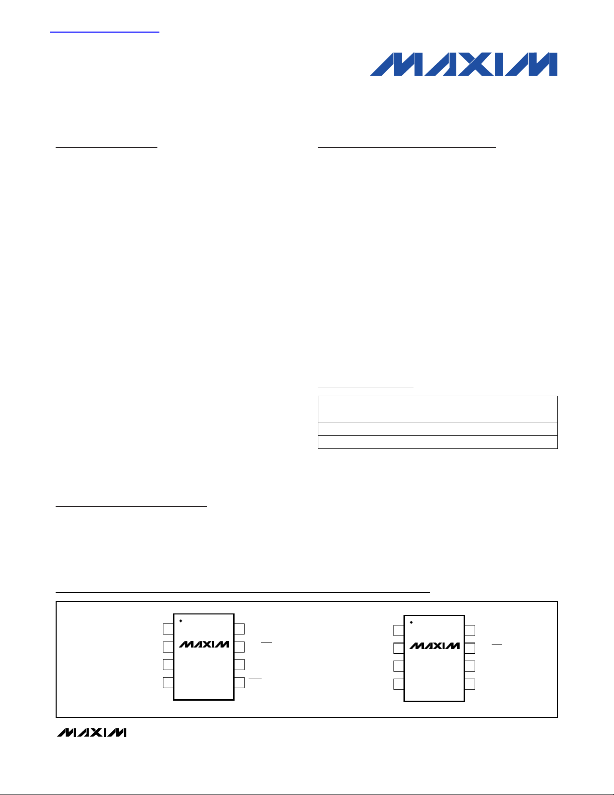
RST/RST
TOP VIEW
µMAX
WDI
WDOGND
1
2
87CLOCK
WDS1
WDS2
V
CC
3
4
6
5
MAX7389
Pin Configurations
Ordering Information
Note: “s” is a placeholder for the reset output type. Insert the
symbol found in Table 3 in the place of “s.” “r” is a placeholder
for the power-on reset (POR) voltage. Insert the symbol found in
Table 2 in the place of “r.” “ff” is a placeholder for the nominal
output frequency. Insert the symbol found in Table 4 in the
place of “ff.” For example, MAX7389CMTP describes a device
with 4.38V reset level, open-collector
RST
output, and a clock
output frequency of 8MHz.
Typical Application Circuit, Functional Diagram, and Selector
Guide appear at end of data sheet.
µMAX is a registered trademark of Maxim Integrated Products, Inc.
WDI
SPEEDGND
1
2
87CLOCK
RST/RSTWDS1
WDS2
V
CC
TOP VIEW
3
4
6
5
MAX7390
µMAX
查询MAX7389供应商
PART TEMP RANGE
o
MAX7389srff -40
MAX7390srff -40oC to +125oC 8 µMAX U8-1
C to +125oC 8 µMAX U8-1
PINPACKAGE
PKG
CODE
Page 2
MAX7389/MAX7390
Microcontroller Clock Generator with
Watchdog
2 _______________________________________________________________________________________
ABSOLUTE MAXIMUM RATINGS
Stresses beyond those listed under “Absolute Maximum Ratings” may cause permanent damage to the device. These are stress ratings only, and functional
operation of the device at these or any other conditions beyond those indicated in the operational sections of the specifications is not implied. Exposure to
absolute maximum rating conditions for extended periods may affect device reliability.
VCCto GND...........................................................-0.3V to +6.0V
All Other Pins to GND ................................-0.3V to (V
CC
+ 0.3V)
CLOCK, RST/RST, WDO Output Current .........................±50mA
Continuous Power Dissipation (T
A
= +70°C)
8-Pin µMAX (derate 4.5mW/°C over +70°C) ................362mW
Operating Temperature Range .........................-40°C to +125°C
Junction Temperature......................................................+150°C
Storage Temperature Range .............................-65°C to +150°C
Lead Temperature (soldering, 10s) .................................+300°C
ELECTRICAL CHARACTERISTICS
(Typical Application Circuit, VCC= +2.7V to +5.5V, TA= -40°C to +125°C, 1MHz to 16MHz output frequency range, typical values at
V
CC
= +5.0V, TA= +25°C, unless otherwise noted.) (Note 1)
PARAMETER SYMBOL CONDITIONS MIN TYP MAX UNITS
POWER REQUIREMENTS
Operating Supply Voltage V
Valid RST/RST Supply Voltage V
Operating Supply Current I
TRI-LEVEL ANALOG INPUTS: WDS1, WDS2
Input-High Voltage Level V
Input-Middle Voltage Level 0.9 VCC - 1.1V V
Input-Low Voltage Level 0.45 V
LOGIC INPUT: WDI
Input Leakage Current I
Logic-Input High Voltage V
Logic-Input Low Voltage V
PUSH-PULL LOGIC OUTPUTS: RST/RST
Output High V
Output Low V
OPEN-DRAIN LOGIC OUTPUTS: RST, PFO, WDO
Output Low V
OUTPUT: CLOCK
Output High Voltage V
Output Low Voltage V
CLOCK Accuracy f
Clock Frequency Temperature
Coefficient
Clock Frequency Supply Voltage
Coefficient
CC
CCR
LEAK
OLO
OHCISOURCE
OLCISINK
CLOCK
TA = 0°C to +85°C 1.1
TA = -40°C to +125°C 1.18
f
CC
CLOCK
f
CLOCK
Input high 0.5 µA
IH
IL
I
OH
SOURCE
I
OL
SINK
I
SINK
TA = 0°C to +85°C, VCC = 5.0V -2.75 +2.75
TA = -40°C to +125°C, VCC = 5.0V -4 +4
V
CC
T
= +25°C (Note 2) 0.67 1 %/V
A
= 12MHz 5.5
= 8MHz 4.5
= 1mA VCC - 1.5 V
= 3mA 0.05 0.4 V
= 3mA 0.05 0.4 V
= 5mA VCC - 0.3 V
= 5mA 0.3 V
= 5.0V (Note 2) 140 400 ppm/°C
2.7 5.5 V
- 0.55V V
C C
0.7 x V
CC
0.3 x V
CC
V
mA
V
V
%
Page 3
MAX7389/MAX7390
Microcontroller Clock Generator with
Watchdog
_______________________________________________________________________________________ 3
ELECTRICAL CHARACTERISTICS (continued)
(Typical Application Circuit, VCC= +2.7V to +5.5V, TA= -40°C to +125°C, 1MHz to 16MHz output frequency range, typical values at
V
CC
= +5.0V, TA= +25°C, unless otherwise noted.) (Note 1)
(
)
(
)
Note 1: All parameters are tested at TA= +25°C. Specifications over temperature are guaranteed by design.
Note 2: Guaranteed by design. Not production tested.
CLOCK Duty Cycle (Note 2) 45 50 55 %
CLOCK Output Jitter
Output Rise Time t
Output Fall Time t
INTERNAL POWER-ON RESET
Reset Voltage
Reset Timeout Period t
WATCHDOG
Watchdog Timeout Period
(Figure 2)
POWER FAIL
Power-Fail Select Threshold V
VCC Monitoring Threshold
Internal Threshold
Internal Threshold Hysteresis V
PFI Monitoring Threshold
External Threshold
External Threshold Hysteresis V
PARAMETER SYMBOL CONDITIONS MIN TYP MAX UNITS
Observation for 20s using a 500MHz
oscilloscope
C
R
C
F
V
V
RST
t
WDG
V
IHYSTVCC
V
EHYST
VCC rising, Table 2
TH+
VCC falling
TH-
Figures 1, 2 86 135 250 µs
WDS1 = GND, WDS2 = GND 11 16 22
WDS1 = open, WDS2 = GND 22 32 44
WDS1 = VCC, WDS2 = GND 44 64 88
WDS1 = GND, WDS2 = open 88 128 177
WDS1 = open, WDS2 = open 177 256 354
WDS1 = VCC, WDS2 = open 354 512 708
WDS1 = GND, WDS2 = V
WDS1 = open, WDS2 = V
W D S 1 = W D S 2 = V
PFI input
SEL
VCC rising 4.06 4.38 4.60 V
ITH
PFI rising 0.9 1.1 1.4 V
ETH
PFI falling 1.0 3.5 8.0 %V
310
= 10p F, 10% to 90% of ful l scal e ( N ote 2) 2.5 7.0 ns
L OA D
= 10p F, 90% to 10% of ful l scal e ( N ote 2) 2.8 7.5 ns
L OA D
V
TA = +25°C
T
= -40°C to +125°C
A
CC
CC
( w atchd og d i sab l ed )
C C
falling 1.0 2 4.0 %V
TH
- 1.5%
V
TH
- 2.5%
0.98 x
V
TH+
708 1024 1416
1416 2048 2832
0.65 x
V
CC
V
TH
+ 1.5%
V
TH
+ 2.5%
0.85 x
V
CC
ps
RMS
V
ms
V
ITH
ETH
Page 4
MAX7389/MAX7390
Microcontroller Clock Generator with
Watchdog
4 _______________________________________________________________________________________
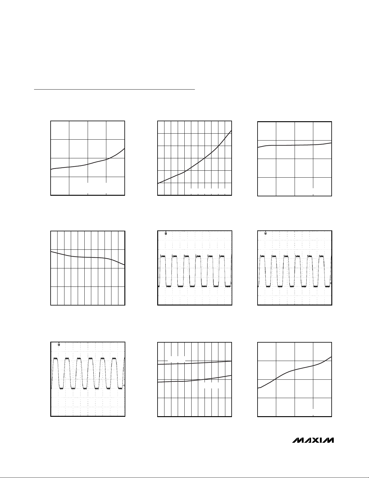
Typical Operating Characteristics
(Typical Application Circuit, VCC= +5V, f
CLOCK
= 16MHz, TA= +25°C, unless otherwise noted.)
DUTY CYCLE vs. TEMPERATURE
MAX7389 toc04
DUTY CYCLE (%)
49
50
51
52
48
TEMPERATURE (°C)
1109580655035205-10-25-40 125
CLOCK OUTPUT WAVEFORM
WITH C
L
= 10pF
MAX7389 toc05
40ns/div
CLOCK
1V/div
VCC = +3.3V
CLOCK OUTPUT WAVEFORM
WITH C
L
= 50pF
MAX7389 toc06
40ns/div
CLOCK
1V/div
VCC = +3.3V
CLOCK OUTPUT WAVEFORM
WITH C
L
= 100pF
MAX7389 toc07
40ns/div
CLOCK
1V/div
SUPPLY CURRENT vs. TEMPERATURE
MAX7389 toc08
I
CC
(mA)
2
3
4
5
1
TEMPERATURE (°C)
1109580655035205-10-25-40 125
VCC = +5V
VCC = +3.3V
SUPPLY CURRENT vs. SUPPLY VOLTAGE
MAX7389 toc09
VCC (V)
I
CC
(mA)
4.854.203.55
2
3
4
5
1
2.90 5.50
V
TH+
= +2.9V
FREQUENCY vs. SUPPLY VOLTAGE
1.020
1.010
1.000
NORMALIZED FREQUENCY
0.990
NORMALIZED TO VCC = +5V
= +2.9V
V
0.980
2.90 5.50
TH+
4.854.203.55
VCC (V)
MAX7389 toc01
1.040
FREQUENCY vs. TEMPERATURE
1.030
1.020
1.010
1.000
NORMALIZED FREQUENCY
0.990
0.980
-40 125
NORMALIZED TO TA = +25°C
TEMPERATURE (°C)
DUTY CYCLE vs. SUPPLY VOLTAGE
52
MAX7389 toc02
51
50
DUTY CYCLE (%)
49
V
1109580655035205-10-25
48
2.90 5.50
VCC (V)
TH+
4.854.203.55
MAX7389 toc03
= +2.9V
Page 5

MAX7389/MAX7390
Microcontroller Clock Generator with
Watchdog
_______________________________________________________________________________________ 5
Typical Operating Characteristics (continued)
(Typical Application Circuit, VCC= +5V, f
CLOCK
= 16MHz, TA= +25°C, unless otherwise noted.)
RESPONSE OF RST AND WDO
WDI EXCEEDING t
WDG
MAX7389/90 toc13
2ms/div
WDO
5V/div
WDI
2V/div
RST
5V/div
t
RST
t
WDG
RISING THRESHOLD vs. TEMPERATURE
MAX7389 toc14
TEMPERATURE (°C)
V
TH+
(V)
1109580655035205-10-25
2.82
2.84
2.86
2.88
2.90
2.80
-40 125
CLOCK RESPONSE TO SPEED SELECT INPUT
MAX7389/90 toc15
200ns/div
SPEED
2V/div
CLOCK
2V/div
CLOCK SETTLING TIME FROM START
1µs/div
MAXIMUM VCC TRANSIENT DURATION
vs. RESET THRESHOLD OVERDRIVE
1000
RESET OCCURS ABOVE THIS CURVE
100
10
TRANSIENT DURATION (µs)
MAX7389 toc10
V
CC
2V/div
CLOCK
2V/div
MAX7389 toc12
POWER-ON RESET BEHAVIOR
100µs/div
MAX7389/90 toc11
t
RST
V
CC
2V/div
CLOCK
5V/div
RST
5V/div
VCC FALLING FROM V
1
100 1000
RESET THRESHOLD OVERDRIVE (mV)
TH+
+ 100mV
900800700600500400300200
Page 6

MAX7389/MAX7390
Microcontroller Clock Generator with
Watchdog
6 _______________________________________________________________________________________
Pin Description
Detailed Description
The MAX7389/MAX7390 replace ceramic resonators,
crystals, and supervisory functions for microcontrollers
in 3.3V and 5V applications.
The MAX7389/MAX7390 provide a clock source, reset,
and watchdog functions. The watchdog timer is pin
programmable and provides watchdog timeout values
in the 16ms to 2048ms range. The MAX7389 provides a
separate watchdog output that is used as a status indicator or to control safety-critical system elements. The
MAX7390 features a clock-speed switch that reduces
the output frequency by half. This functionality allows
the microcontroller to operate at reduced power and
may be used to extend the time available to perform
housekeeping tasks, such as writing data to flash during
a power failure.
The integrated reset and watchdog functions provide the
power-supply monitoring functions necessary to ensure
correct microcontroller operation. The reset circuit has
built-in power-supply transient immunity and provides
both power-on reset and power-fail or brownout reset
functionality. Two standard factory-trimmed reset levels
are available. The watchdog timer is programmable to
eight individual timeout values and may be disabled for
test purposes.
Clock Output (CLOCK)
The push-pull clock output (CLOCK) drives a groundconnected 1kΩ load or a positive supply connected
500Ω load to within 300mV of either supply rail. CLOCK
remains stable over the full operating voltage range and
does not generate short output cycles during either
power-on or power-off. A typical startup characteristic is
shown in the Typical Operating Characteristics section.
The MAX7390 clock output frequency is reduced by a
factor of two by taking SPEED low. This functionality
allows the microcontroller to operate at reduced power
and may be used to extend the time available to perform housekeeping tasks.
Reset
The reset function drives the microcontroller reset input
to prevent operation in the cases of the initial power-on
setting, low power-supply voltages, and the failed
PIN
MAX7389 MAX7390
11V
2 2 WDS1
3 3 WDS2
4 4 GND Ground
5 ⎯ WDO
— 5 SPEED
NAME FUNCTION
Power Input. Connect VCC to the power supply. Bypass VCC to GND with a 1µF capacitor.
CC
Install the bypass capacitor as close to the device as possible.
Watchdog Timeout Select Input 1. Connect WDS1 and WDS2 to V
shown in Table 1, to set the watchdog timeout period.
Watchdog Timeout Select Input 2. Connect WDS2 and WDS1 to V
shown in Table 1, to set the watchdog timeout period.
Watchdog Output. Open-drain watchdog output asserts if WDI is not toggled within the
watchdog timeout period.
Clock-Speed Select Input. Connect SPEED high for the factory-trimmed clock output
frequency. Connect SPEED low to reduce the clock output frequency by half.
, GND, or VCC/2, as
CC
, GND, or VCC/2, as
CC
6 6 WDI
7 7 RST/RST
8 8 CLOCK Clock Output
Watchdog Input. A rising edge on WDI resets watchdog timer. If WDI does not receive a
rising edge within the watchdog timeout period (t
timeout period is programmable through WDS1 and WDS2. Connect WDS1 and WDS2 to
V
to disable the watchdog timer.
CC
Reset Output. Reset output is available in one of three configurations: push-pull RST, pushpull RST, or open-drain RST. The reset output is asserted if one of the following conditions
occurs: whenever V
asserts when WDI does not receive a rising edge within the watchdog timeout period.
), RST/RST asserts. The watchdog
WDG
is below the reset threshold level; for devices with WDI, reset output
CC
Page 7

watchdog operations. Three reset output versions are
available: push-pull RST, push-pull RST, and open-drain
RST. The reset timeout period (t
RST
) is nominally 135s.
Power-On Reset (POR)
The internal power-on reset (POR) circuit detects the
power-supply voltage (VCC) level at startup. The POR
circuit starts the oscillator when VCCexceeds the reset
rising threshold level (V
TH+
). The reset output remains
asserted from the time VCCcrosses the V
TH+
and con-
tinues to be asserted for the reset timeout period (t
RST
).
Upon completion of the reset timeout, the reset output
is released. See Figure 1.
Low-Voltage Lockout
The reset output asserts whenever VCCdrops below the
reset falling threshold, V
TH-
. The difference between the
reset rising and falling threshold values is V
TH+
- (V
TH-
).
The nominal hysteresis value is 2% of the reset rising
threshold value. The reset detection circuitry provides
filtering to prevent triggering on negative voltage spikes.
See the Typical Operating Characteristics for a plot of
maximum transient duration without causing a reset
pulse vs. reset comparator overdrive.
Figure 1 shows the reset output (RST/RST) behavior
during power-up and brownout.
Watchdog
The watchdog function provides microprocessor monitoring by requiring the microprocessor to toggle an output pin to indicate correct operation. The WDI input
monitors the port signal and resets the watchdog timer
on receipt of a rising edge. If an edge is not received
within the required watchdog timeout period, the watchdog circuit initiates a reset cycle and asserts the WDO
output (MAX7389 only). The internal watchdog circuits
are reset and the watchdog timer restarts at the end of
the reset cycle (RST/RST output releases). The WDO
output remains asserted until a valid edge is received
on the WDI input, signifying correct microprocessor
operation. The WDO output can be used as a status
indicator either to the microprocessor or to an external
device, such as a fault-indicating LED or sounder. The
MAX7389/MAX7390
Microcontroller Clock Generator with
Watchdog
_______________________________________________________________________________________ 7
Figure 1. RST/
RST
Behavior During Power-Up and Brownout
5
4
V
(V)
CC
V
3
2
TH+
V
TH-
CLK
RST
CLOCK STARTS ON INTERNAL
POR (V
RST RELEASES AFTER THE
RESET TIMEOUT PERIOD.
RST ASSERTS ON RESET FALLING
VOLTAGE (V
CLOCK STOPS.
RST CONTINUES TO
ASSERT UNTIL V
1
t
RST
, VCC RISING).
TH+
, VCC FALLING).
TH-
.
CCR
V
CCR
Page 8

Figure 2. Watchdog Timing Diagram
MAX7389/MAX7390
WDO output is an open-drain output. The power-up
condition of the WDO output is high (not asserted).
The operation of the watchdog and reset function is
illustrated in Figure 2.
The watchdog timeout period is set to one of nine possible values by pin strapping WDS1 and WDS2. Each
control input has three possible values assigned by
connection to GND, V
CC
, or VCC/2 (see Table 1). One
of the assigned values disables the watchdog function
and is intended for customer use during test. The
watchdog timer is disabled while the RST/RST output is
asserted.
Applications Information
Interfacing to a Microcontroller
Clock Input
The CLOCK output is a push-pull, CMOS logic output,
which directly drives any microprocessor (µP) or microcontroller (µC) clock input. There are no impedancematching issues when using the MAX7389/MAX7390.
Operate the MAX7389/MAX7390 and microcontroller
(or other clock input device) from the same supply voltage level. Refer to the microcontroller data sheet for
clock-input compatibility with external clock signals.
The MAX7389/MAX7390 require no biasing components
or load capacitance. When using the MAX7389/
MAX7390 to retrofit a crystal oscillator, remove all biasing
components from the oscillator input.
Power-Supply Considerations
The MAX7389/MAX7390 operate with power-supply
voltages in the 2.7V to 5.5V range. Power-supply
decoupling is needed to maintain the power-supply
rejection performance of the devices. Bypass VCCto
GND with a 0.1µF surface-mount ceramic capacitor.
Mount the bypass capacitor as close to the device as
possible. If possible, mount the MAX7389/MAX7390
close to the microcontroller’s decoupling capacitor so
that additional decoupling is not required.
A larger-value bypass capacitor is recommended if the
MAX7389/MAX7390 are to operate with a large capacitive load. Use a bypass capacitor value of at least 1000
times that of the output load capacitance.
Microcontroller Clock Generator with
Watchdog
8 _______________________________________________________________________________________
Table 1. Watchdog Timeout Periods
Note: WDS1 or WDS2 is pulled internally to VCC/2 if left floating.
WATCHDOG TIMEOUT
WDS1 WDS2
GND GND 11 16 22
VCC/2 = open GND 22 32 44
V
CC
GND VCC/2 = open 88 128 177
VCC/2 = open VCC/2 = open 177 256 354
V
CC
GND V
VCC/2 = open V
V
CC
GND 44 64 88
VCC/2 = open 354 512 708
CC
CC
V
CC
PERIOD (ms)
MIN TYP MAX
708 1024 1416
1416 2048 2828
Disabled
V
CC
CLK
RST
INTERNAL
WATCHDOG STATE
WDI
WDO
ACTIVE
TRIPPED
WATCHDOG TIMEOUT
PERIOD (t
WDG
)
RESET TIMEOUT PERIOD
(t
RST
)
Page 9

Output Jitter
The MAX7389/MAX7390s’ jitter performance is given in
the Electrical Characteristics table as a peak-to-peak
value obtained by observing the output of the device for
20s with a 500MHz oscilloscope. Jitter measurements
are approximately proportional to the period of the output frequency of the device. Thus, a 4MHz part has
approximately twice the jitter value of an 8MHz part.
The jitter performance of all clock sources degrades in
the presence of mechanical and electrical interference.
The MAX7389/MAX7390 are immune to vibration,
shock, and EMI influences and thus provide a considerably more robust clock source than crystal- or ceramicresonator-based oscillator circuits.
MAX7389/MAX7390
Microcontroller Clock Generator with
Watchdog
_______________________________________________________________________________________ 9
Table 2. POR Voltage
Note: Standard values are shown in bold. Contact factory for
other POR voltage.
Table 3. Reset Output Type
Table 4. Clock Output Frequency
Note: Contact factory for other frequencies.
Note: Other versions with different features are available. Refer to the MAX7387/MAX7388 and MAX7391 data sheets.
Selector Guide
(
)
(
)
(
)
Note: Standard values are shown in bold. Contact factory for
other output types.
POWER-ON RESET VOLTAGE (VTH) r
4.38 M
3.96 J
3.44 N
3.34 P
3.13 Q
2.89 S
2.82 V
2.5 X
OUTPUT TYPE s
Push-pull RST A
Push-pull RST B
Open drain RST C
CLOCK FREQUENCY (f
4RD
8TP
12 VB
16 WB
) (MHz) ff
CLOCK
PART
MAX7387 1 to 16 Yes Yes/yes Yes/yes — 10 µMAX
MAX7388 1 to 16 Yes Yes/no No/yes — 8 µMAX
MAX7389 1 to 16 Yes Yes/yes No/no — 8 µMAX
MAX7390 1 to 16 Yes Yes/no No/no Yes 8 µMAX
MAX7391 1 to 16 Yes No/no Yes/no Yes 8 µMAX
FREQUENCY
RANGE
MHz
RESET
FUNCTION
WATCHDOG INPUT (WDI)/
WATCHDOG OUTPUT
WDO
POWER-FAIL INPUT (PFI)/
POWER-FAIL OUTPUT
PFO
SPEED
PACKAGE
PIN-
Page 10

MAX7389/MAX7390
Microcontroller Clock Generator with
Watchdog
10 ______________________________________________________________________________________
Functional Diagram
Typical Application Circuit
Chip Information
PROCESS: BiCMOS
V
CC
MAX7389
MAX7390
RST/RST
POWER-ON
RESET
WDI
WDS1
WDS2
12V
*MAX7389 ONLY
**MAX7390 ONLY
5V
DC-DC
WDS1
OSCILLATOR
V
CC
RST/RST
PRESCALER
WATCHDOG
TIMER
GND
RESET TIMER
CLOCK
SPEED**
WDO*
N
V
RST/RST
CC
*MAX7389 ONLY
**MAX7390 ONLY
WDS2
MAX7389
MAX7390
GND
WDO*
WDI
SPEED**
CLOCK
I/O PORT
I/O PORT
I/O PORT
OSC1
µC
Page 11
MAX7389/MAX7390
Microcontroller Clock Generator with
Watchdog
Maxim cannot assume responsibility for use of any circuitry other than circuitry entirely embodied in a Maxim product. No circuit patent licenses are
implied. Maxim reserves the right to change the circuitry and specifications without notice at any time.
Maxim Integrated Products, 120 San Gabriel Drive, Sunnyvale, CA 94086 408-737-7600 ____________________ 11
© 2006 Maxim Integrated Products Printed USA is a registered trademark of Maxim Integrated Products, Inc.
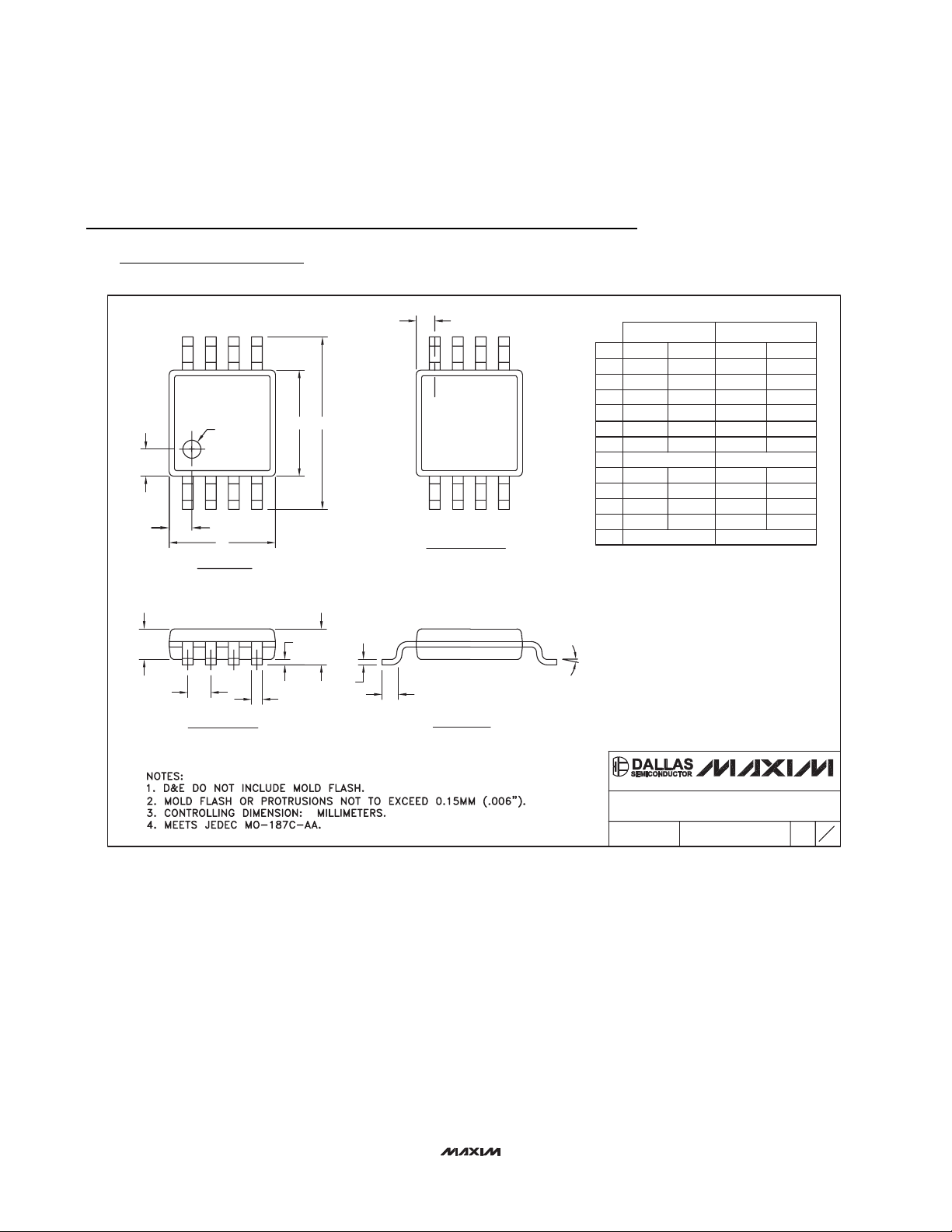
Package Information
(The package drawing(s) in this data sheet may not reflect the most current specifications. For the latest package outline information,
go to www.maxim-ic.com/packages
.)
8
Ø0.50±0.1
0.6±0.1
0.6±0.1
1
D
TOP VIEW
A2
E H
A1
4X S
BOTTOM VIEW
A
8
1
DIM
A
A1
A2
b
c
D
e
E
H
L
α
S
INCHES
MIN
-
0.002
0.030
0.010
0.005
0.116
0.0256 BSC
0.116
0.188
0.016
0°
0.0207 BSC
MAX
0.043
0.006
0.037
0.014
0.007
0.120
0.120
0.198
0.026
6°
MILLIMETERS
MIN
0.05 0.15
0.25 0.36
0.13 0.18
2.95 3.05
2.95 3.05
4.78
0.41
MAX
- 1.10
0.950.75
0.65 BSC
5.03
0.66
0.5250 BSC
6°0°
8LUMAXD.EPS
e
FRONT VIEW
c
b
L
SIDE VIEW
α
PROPRIETARY INFORMATION
TITLE:
PACKAGE OUTLINE, 8L uMAX/uSOP
REV.DOCUMENT CONTROL NO.APPROVAL
21-0036
1
J
1
 Loading...