

Page 1
现货库存、技术资料、百科信息、热点资讯,精彩尽在鼎好!
General Description
The MAX7384 dual-speed silicon oscillator replaces
ceramic resonators, crystals, and crystal-oscillator
modules as the primary and secondary clock source for
microcontrollers in 3V, 3.3V, and 5V applications. The
MAX7384 features a factory-programmed high-speed
oscillator, a 32.768kHz oscillator, a clock-selector input,
and a µP power-on-reset (POR) supervisor. The clock
output can be switched at any time between the highspeed clock and the 32.768kHz clock for low-power
operation. Switchover is synchronized internally to provide glitch-free clock switching.
Unlike typical crystal and ceramic-resonator oscillator
circuits, the MAX7384 is resistant to vibration and EMI.
The high-output-drive current and absence of highimpedance nodes makes the oscillator less susceptible
to dirty or humid operating conditions. With a wide operating temperature range as standard, the MAX7384 is a
good choice for demanding home appliance, industrial,
and automotive environments.
The MAX7384 is available with factory-programmed frequencies ranging from 10MHz to 16MHz. See Table 1
for standard frequencies and contact the factory for
custom frequencies. Refer to the MAX7378 data sheet
for frequencies less than 10MHz.
The MAX7384 is available in an 8-pin µMAX®package.
The MAX7384 standard operating temperature range is
-40°C to +125°C. See the Applications Information section for extended operating temperature range.
Applications
White Goods
Automotive
Consumer Products
Appliances and Controls
Handheld Products
Portable Equipment
Microcontroller Systems
Features
♦ 2.7V to 5.5V Operation
♦ High-Speed Oscillator from 10MHz to 16MHz
Low-Speed 32kHz Oscillator
Glitch-Free Clock-Speed Switching
♦ Integrated POR
♦ ±10mA Clock-Output Drive Capability
♦ 2.5% Initial Accuracy
♦ ±50ppm/°C Frequency Drift
♦ 50% Duty Cycle
♦ 5ns Output Rise and Fall Time
♦ Low Jitter: 80ps
P-P
at 16MHz
♦ 4mA Operating Current at 16MHz
♦ 13µA, 32kHz Operating Current
♦ -40°C to +125°C Temperature Range
MAX7384
Silicon Oscillator with Low-Power Frequency
Switching and Reset Output
________________________________________________________________ Maxim Integrated Products 1
Ordering Information
OSC1
OSC2
RST
µC
GND
RST/RST
CLOCK
E.C.
V
CC
0.1µF
V
CC
2.7V TO 5.5V
MAX7384
V
L
0.1µF
I/O PORT
SPEED
Typical Application Circuit
19-3493; Rev 0; 11/04
For pricing, delivery, and ordering information, please contact Maxim/Dallas Direct! at
1-888-629-4642, or visit Maxim’s website at www.maxim-ic.com.
*Standard version is shown in bold. The first letter after the part
number designates the reset output option. Insert the letter
corresponding to the desired reset threshold level from Table 1
in the next position. Insert the two-letter code from Table 2 in
the remaining two positions for the desired frequency range.
Table 1 and Table 2 are located at the end of the data sheet.
Pin Configuration appears at end of data sheet.
µMAX is a registered trademark of Maxim Integrated Products, Inc.
PART* TEMP RANGE
MAX7384A_ _ _ -40°C to +125°C8 µMAX
MAX7384B_ _ _ -40°C to +125°C8 µMAX
MAX7384C_ _ _ -40°C to +125°C8 µMAX Open drain
PINPACKAGE
RESET
OUTPUT
Active high
push-pull
Active low
push-pull
Page 2
MAX7384
Silicon Oscillator with Low-Power Frequency
Switching and Reset Output
2 _______________________________________________________________________________________
ABSOLUTE MAXIMUM RATINGS
Stresses beyond those listed under “Absolute Maximum Ratings” may cause permanent damage to the device. These are stress ratings only, and functional
operation of the device at these or any other conditions beyond those indicated in the operational sections of the specifications is not implied. Exposure to
absolute maximum rating conditions for extended periods may affect device reliability.
VCCto GND...........................................................-0.3V to +6.0V
All Other Pins to GND.................................-0.3V to (V
CC
+ 0.3V)
CLOCK, RST Current .......................................................±50mA
Input Current (SPEED)......................................................±50mA
Continuous Power Dissipation (T
A
= +70°C)
8-Pin µMAX (derate 4.5mW/°C above +70°C) ...362mW (U8-1)
Operating Temperature Range .........................-55°C to +135°C
Junction Temperature......................................................+150°C
Storage Temperature Range .............................-65°C to +150°C
Lead Temperature (soldering, 10s) .................................+300°C
ELECTRICAL CHARACTERISTICS
(Typical Operating Circuit, VCC= 2.7V to 5.5V, VL= VCC, TA= -40°C to +125°C. Typical values are at VCC= 5.0V, TA= +25°C,
unless otherwise noted.) (Note 1)
Operating Supply Voltage V
Operating Supply Current I
LOGIC INPUTS (SPEED)
Input High Voltage V
Input Low Voltage V
Input Current I
CLOCK OUTPUT
Output High Voltage V
Output Low Voltage V
Initial Fast Clock Frequency
Accuracy
Fast Clock Temperature
Coefficient
PARAMETER SYMBOL CONDITIONS MIN TYP MAX UNITS
CC
f
= 16MHz, TA = -40°C to +125°C, no
CLOCK
load
f
= 14.7456MHz, TA = -40°C to
CLOCK
+125°C, no load
f
= 12MHz, TA = -40°C to +125°C, no
CLOCK
CC
IN
OH
OL
f
CLOCK
load
f
= 11.0592MHz, TA = -40°C to
CLOCK
+125°C, no load
f
= 10MHz, TA = -40°C to +125°C, no
CLOCK
load
f
= 32.768kHz, TA = -40°C to
CLOCK
+125°C, no load
IH
IL
V
= SPEED = 5.5V 2
CC
VL = 4.5V, I
VL = 2.7V, I
VL = 4.5V, I
VL = 2.7V, I
VCC = 5V, TA = +25°C, deviation from
selected frequency
VCC = 2.7V to 5.5V, TA = +25°C,
deviation from selected frequency
T
= -40°C to +125°C ±50 ±350 ppm/°C
A
SOURCE
SOURCE
SINK
SINK
2.7 5.5 V
8.7
8.0
6.5
6.0
5.4
13 25 µA
0.7 x V
CC
0.3 x V
CC
= 7.0mA
= 2.0mA
= 20mA
= 10mA
- 0.4 V
V
L
0.4 V
-2.5 +2.5
-5 +3.5
mA
V
µA
%
Page 3
MAX7384
Silicon Oscillator with Low-Power Frequency
Switching and Reset Output
_______________________________________________________________________________________ 3
ELECTRICAL CHARACTERISTICS (continued)
(Typical Operating Circuit, VCC= 2.7V to 5.5V, VL= VCC, TA= -40°C to +125°C. Typical values are at VCC= 5.0V, TA= +25°C,
unless otherwise noted.) (Note 1)
Note 1: All parameters tested at TA= +25°C. Specifications over temperature are guaranteed by design.
Note 2: Guaranteed by design. Not production tested.
Note 3: For push-pull output only.
Slow Clock Frequency f
Slow Clock Temperature
Coefficient
Duty Cycle (Note 2) 40 50 60 %
Output Jitter
Output Rise Time t
Output Fall Time t
Power-On-Reset Threshold V
Power-On-Reset Hysteresis V
Power-On-Reset Delay PORdly VCC rising from 0 to 5V in 1µs at +25°C 122 µs
RESET OUTPUT
Output High Voltage
(Note 3)
Output Low Voltage V
PARAMETER SYMBOL CONDITIONS MIN TYP MAX UNITS
CLOCK
R
F
TH
HYST
V
OH
OL
VCC = 5V, TA = +25°C 32.268 32.768 33.268
VCC = 2.7V to 5.5V, TA = +25°C 31.768 32.768 33.768
= -40°C to +125°C ±50 ±325 ppm/°C
T
A
Observation of 16MHz for 20s using a
12GHz oscilloscope
10% to 90% 5 ns
90% to 10% 5 ns
VCC rising, deviation
from nominal threshold
Difference between rising and falling
thresholds
VL = 4.5V, I
VL = 2.7V, I
VL = 4.5V, I
VL = 2.7V, I
SOURCE
SOURCE
= 20mA 0.4
SINK
SOURCE
TA = +25°C -2 +2
T
= -40°C to
A
+125°C
= 7.0mA
= 2.0mA
= 10mA 0.4
-5 +5
V
CC
0.4
V
CC
0.4
80 ps
1%
-
-
kHz
P-P
%
V
V
Page 4

MAX7384
Silicon Oscillator with Low-Power Frequency
Switching and Reset Output
4 _______________________________________________________________________________________
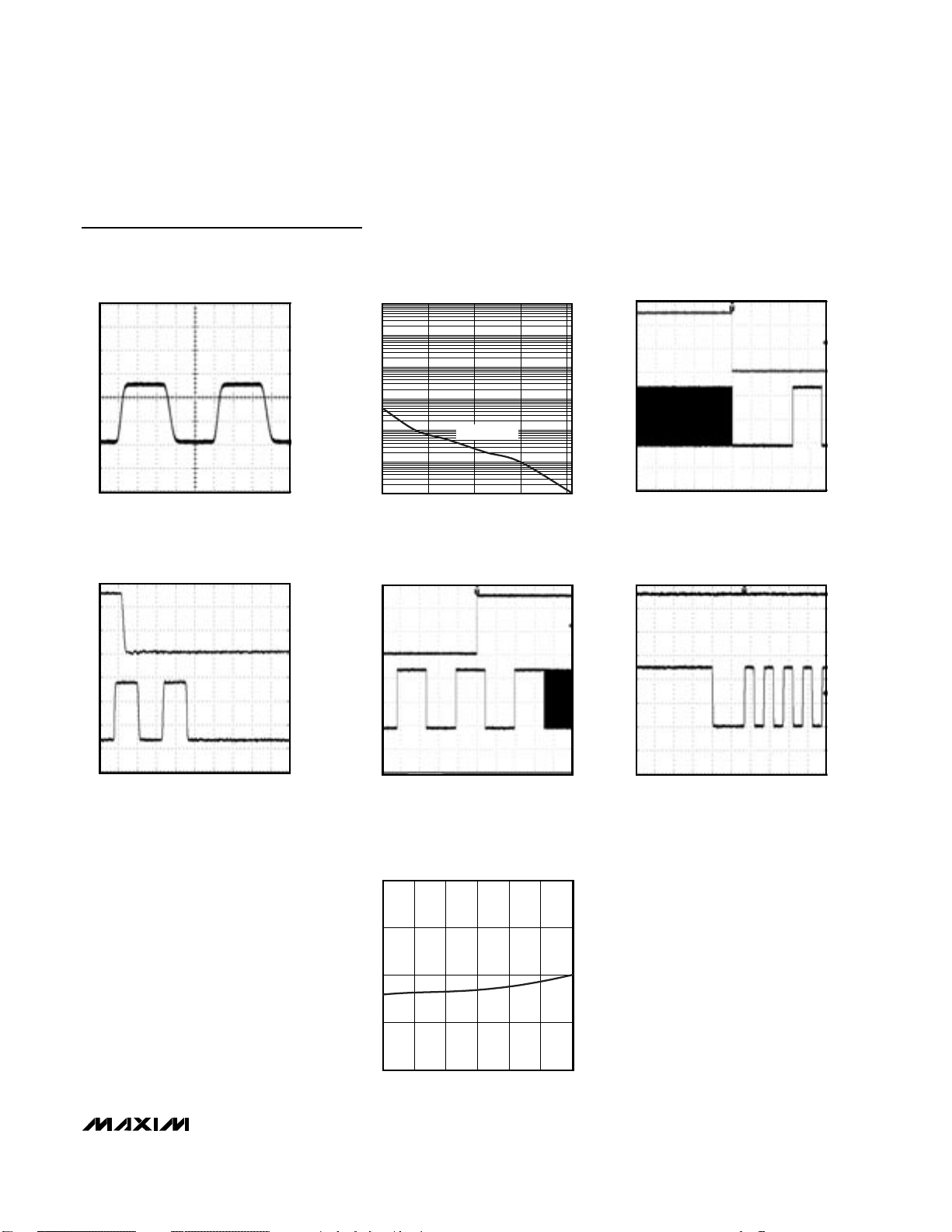
Typical Operating Characteristics
(VCC= VL= 5V, TA= +25°C, frequency = 10MHz, unless otherwise noted.)
48.0
48.5
49.5
49.0
50.0
50.5
-55 21-17 59 97 135
DUTY CYCLE vs. TEMPERATURE
MAX7384 toc01
TEMPERATURE (°C)
DUTY CYCLE (%)
FREQUENCY = 10MHz
45
47
46
49
48
50
51
2.7 3.9 4.33.1 3.5 4.7 5.1 5.5
DUTY CYCLE vs. SUPPLY VOLTAGE
MAX7384 toc02
SUPPLY VOLTAGE (V)
DUTY CYCLE (%)
FREQUENCY = 11.0592MHz
2.90
3.00
2.95
3.10
3.05
3.20
3.15
3.25
-55 21 59-17 97 135
SUPPLY CURRENT vs. TEMPERATURE
MAX7384 toc03
TEMPERATURE (°C)
SUPPLY CURRENT (mA)
FREQUENCY = 10MHz
1.5
2.0
3.0
2.5
3.5
4.0
2.7 3.53.1 3.9 4.3 4.7 5.1 5.5
SUPPLY CURRENT
vs. SUPPLY VOLTAGE
MAX7384 toc04
SUPPLY VOLTAGE (V)
SUPPLY CURRENT (mA)
FREQUENCY = 11.0592MHz
-2.0
-1.0
-1.5
0
-0.5
1.5
1.0
0.5
2.0
2.7 3.53.1 3.9 4.3 4.7 5.1 5.5
FREQUENCY DEVIATION
vs. SUPPLY VOLTAGE
MAX7384 toc05
SUPPLY VOLTAGE (V)
PERCENT (%)
FREQUENCY = 11.0592MHz
-4
-3
-2
-1
0
1
2
3
4
-55 -17 21 59 97 135
FREQUENCY DEVIATION
vs. TEMPERATURE
MAX7384 toc06
TEMPERATURE (°C)
PERCENT (%)
FREQUENCY = 10MHz
CHANNEL 1 = CLOCK, CHANNEL 2 = V
CC
10µs/div
SETTLING TIME FROM START
MAX7384 toc07
CH1 FREQ
9.992MHz
LOW RESOLUTION
CLOCK OUTPUT WAVEFORM
(C
L
= 10pF)
MAX7384 toc08
20ns/div
CLOCK OUTPUT WAVEFORM
(C
L
= 50pF)
MAX7384 toc09
20ns/div
Page 5
MAX7384
Silicon Oscillator with Low-Power Frequency
Switching and Reset Output
_______________________________________________________________________________________ 5
Typical Operating Characteristics (continued)
(VCC= VL= 5V, TA= +25°C, frequency = 10MHz, unless otherwise noted.)
CLOCK OUTPUT WAVEFORM
= 100pF)
(C
L
20ns/div
HIGH-SPEED TO LOW-SPEED
TRANSITION
MAX7384 toc10
MAXIMUM TRANSIENT DURATION (s)
MAX7384 toc13
MAXIMUM TRANSIENT DURATION
vs. RESET THRESHOLD OVERDRIVE
1
0.1
0.01
1m
10m
100m
1µ
0.04 0.24
RESET THRESHOLD OVERDRIVE (V)
0.09
V
RESET
0.14
= 4.32V
LOW-SPEED TO HIGH-SPEED
TRANSITION
0.19
MAX7384 toc14
MAX7384 toc11
HIGH-SPEED TO LOW-SPEED
TRANSITION
10µs/div
CHANNEL 1 = CLOCK, CHANNEL 2 = SPEED
MAX7384 toc12
LOW-SPEED TO HIGH-SPEED
TRANSITION
MAX7384 toc15
40ns/div
CHANNEL 1 = CLOCK, CHANNEL 2 = SPEED
10µs/div
CHANNEL 1 = CLOCK, CHANNEL 2 = SPEED
SUPPLY CURRENT vs. FREQUENCY
5
4
3
SUPPLY CURRENT (mA)
2
1
10 1311 12 14 15 16
FREQUENCY (MHz)
100ns/div
CHANNEL 1 = CLOCK, CHANNEL 2 = SPEED
MAX7384 toc16
Page 6
MAX7384
Detailed Description
The MAX7384 is a dual-speed clock generator with integrated reset for microcontrollers (µCs) and UARTs in 3V,
3.3V, and 5V applications. The MAX7384 is a replacement for crystal-oscillator modules, crystals, or ceramic
resonators and a system reset IC. The high-speed clock
frequency and reset threshold voltage are factory
trimmed to specific values (see Table 1). A variety of
popular standard frequencies are available. The lowspeed clock frequency is fixed at 32.768kHz; see Table
2. No external components are required for setting or
adjusting the frequency.
Oscillator
The push-pull clock output drives a load to within
400mV of either supply rail. The clock output remains
stable over the full operating voltage range and does
not generate short output cycles during either power-on
or changing of the frequency. A typical oscillating startup is shown in the Typical Operating Characteristics.
Clock-Speed Selection
Drive SPEED low to select slow clock speed (nominally
32.768kHz) or high to select full clock speed. SPEED can
be connected to VCCor to GND to select fast or slow
clock speed, or connected to a logic output (such as a µP
GPIO port) used to change clock speed on the fly. If
SPEED is connected to a µP GPIO port, connect a pullup
or pulldown resistor to set the clock to the preferred
speed on power-up. SPEED input bias current is 2µA
(max), so a resistor value as high as 500kΩ can be used.
Applications Information
Interfacing to a Microcontroller
Clock Input
The MAX7384 clock output is a push-pull, CMOS, logic
output that directly drives a µP or µC clock input. There
are no impedance-matching issues when using the
MAX7384. Refer to the microcontroller data sheet for
clock input compatibility with external clock signals.
The MAX7384 requires no biasing components or load
capacitance. When using the MAX7384 to retrofit a
crystal oscillator, remove all biasing components from
the oscillator input.
Reset Output
The MAX7384 is available with three reset output stage
options: push-pull active low, push-pull active high, and
open-drain active low. RST is asserted when the monitored input (VCC) drops below the internal V
TH-
threshold
and remains asserted for 120µs after the monitored input
exceeds the internal V
TH+
threshold. The open-drain
RST output requires an external pullup resistor.
Output Jitter
The MAX7384’s jitter performance is given in the
Electrical Characteristics table as a peak-to-peak value
obtained by observing the output of the MAX7384 for
Silicon Oscillator with Low-Power Frequency
Switching and Reset Output
6 _______________________________________________________________________________________
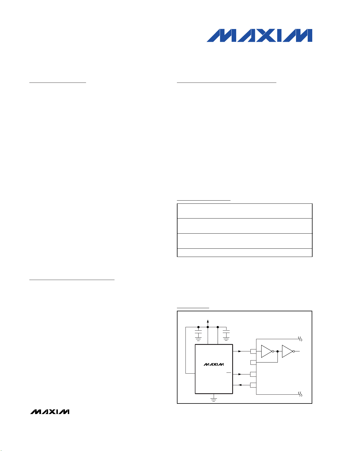
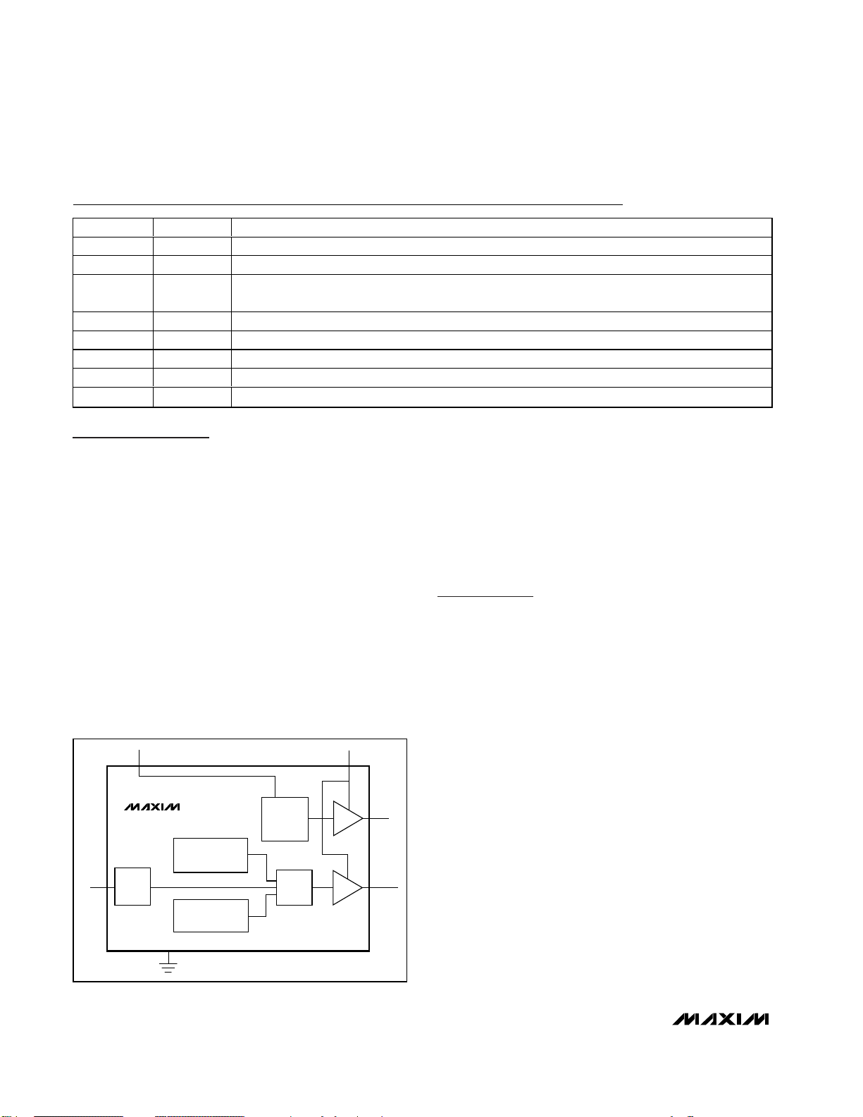
Figure 1. Functional Diagram
Pin Description
PIN
1VCCPositive Supply Voltage. Bypass VCC to GND with a 0.1µF capacitor.
2V
3 SPEED
4 RST Reset Output. Open-drain or push-pull output. See the Ordering Information.
5 CLOCK Push-Pull Clock Output
6 GND Ground
7 E.C. Externally Connected. Connect to Vcc.
8 N.C. No Connection. Not internally connected.
NAME
L
Output Supply Voltage. Bypass VL to GND with a 0.1µF capacitor. VL must be connected to VCC.
Clock-Speed Select Input. Drive SPEED low to select the 32kHz fixed frequency. Drive SPEED high
to select factory-trimmed frequency.
2.7V TO 5.5V
V
CC
V
L
FUNCTION
RST
CLOCK
SPEED
LOGIC
MAX7384
32kHz
(LF OSCILLATOR)
10MHz TO 16MHz
(HF OSCILLATOR)
GND
POR
MUX
Page 7
20s with a 12GHz oscilloscope. Jitter measurements
are approximately proportional to the output period of
the device. Thus, a 10MHz device has approximately
twice the jitter value of a 20MHz device. The jitter performance of all clock sources degrades in the presence of mechanical and electrical interference. The
MAX7384 is relatively immune to vibration, shock, and
EMI influences and thus provides a considerably more
robust clock source than crystal or ceramic resonatorbased oscillator circuits.
Initial Power-Up and Operation
An internal power-up reset asserts RST until the supply
voltage has risen above the power-on-reset threshold
(V
TH+
).
RST holds the microcontroller in a reset condition until
120µs after VCChas risen above V
TH+
. This reset delay
ensures that the clock output and the microcontroller’s
internal clock circuits have stabilized before the system
is allowed to start. Typical microcontroller reset delay
ranges from 1ms to 250ms to allow a slow crystal oscillator circuit to start up. The MAX7384 has a fast startup,
eliminating the need for such a long reset delay.
Extended Temperature Operation
The MAX7384 was tested to +135°C during product characterization and shown to function normally at this temperature (see the Typical Operating Characteristics).
However, production test and qualification is only performed from -40°C to +125°C at this time. Contact the factory if operation outside this range is required.
Power-Supply Considerations
The MAX7384 operates with a 2.7V and 5.5V powersupply voltage. VCCprovides power to the the internal
circuitry and VLsupplies power to the clock and reset
outputs. Good power-supply decoupling is needed to
maintain the power-supply rejection performance of the
MAX7384. Bypass both V
CC
and VLto GND with a
0.1µF surface-mount ceramic capacitor. Mount the
bypassing capacitors as close to the device as possible. Use a larger value bypass capacitor if the MAX7384
is to operate with a large capacitive load. Use a bypass
capacitor value of at least 1000 times that of the output
load capacitance.
MAX7384
Silicon Oscillator with Low-Power Frequency
Switching and Reset Output
_______________________________________________________________________________________ 7
Table 3. Standard Part Numbers
Table 1. Standard Reset Threshold
Levels
Table 2. Standard Frequencies
Contact factory for nonstandard reset threshold options.
For all other frequency options, contact factory.
SUFFIX RESET THRESHOLD (V)
X 2.50
V 2.71
R 2.89 Standard value
Q 3.13
P 3.34
N 3.44
J 3.96
M 4.38 Standard value
SUFFIX STANDARD FREQUENCY (MHz)
UK 10
UT 11.0592
VB 12
VT 14.7456
WB 16
PART
MAX7384CRUK Open drain 2.89 10
MAX7384CRUT Open drain 2.89 11.0592
MAX7384CRVB Open drain 2.89 12
MAX7384CRVT Open drain 2.89 14.7456
MAX7384CRWB Open drain 2.89 16
MAX7384CMUK Open drain 4.38 10
MAX7384CMUT Open drain 4.38 11.0592
MAX7384CMVB Open drain 4.38 12
MAX7384CMVT Open drain 4.38 14.7456
MAX7384CMWB Open drain 4.38 16
RESET
OUTPUT
TYPE
RESET
THRESHOLD
(V)
FREQUENCY
(MHz)
Page 8

MAX7384
Silicon Oscillator with Low-Power Frequency
Switching and Reset Output
8 _______________________________________________________________________________________
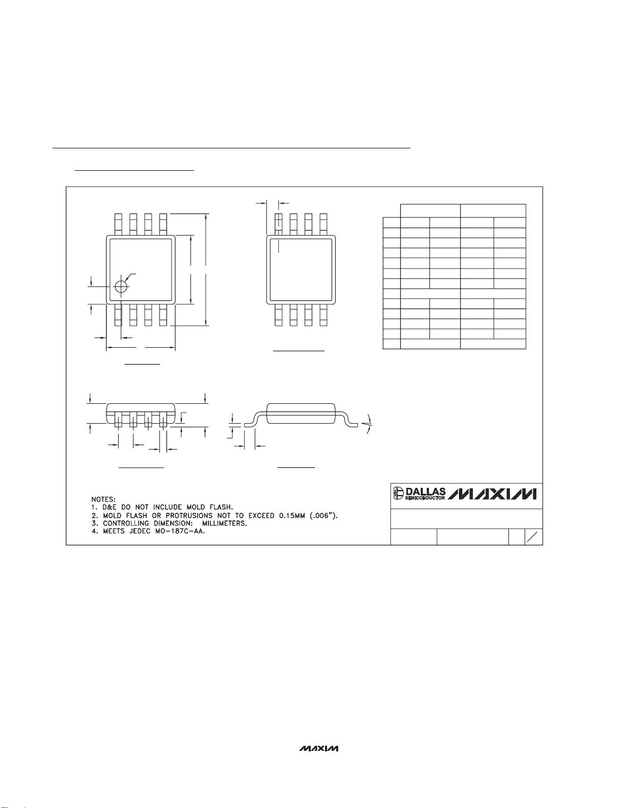
Pin Configuration
Chip Information
TRANSISTOR COUNT: 2937
PROCESS: BiCMOS
TOP VIEW
V
SPEED
1
CC
2
L
MAX7384
3
4
µMAX
87N.C.
E.C.V
GND
6
CLOCKRST
5
Page 9
MAX7384
Silicon Oscillator with Low-Power Frequency
Switching and Reset Output
Maxim cannot assume responsibility for use of any circuitry other than circuitry entirely embodied in a Maxim product. No circuit patent licenses are
implied. Maxim reserves the right to change the circuitry and specifications without notice at any time.
Maxim Integrated Products, 120 San Gabriel Drive, Sunnyvale, CA 94086 408-737-7600 _____________________ 9
© 2004 Maxim Integrated Products Printed USA is a registered trademark of Maxim Integrated Products.
Package Information
(The package drawing(s) in this data sheet may not reflect the most current specifications. For the latest package outline information,
go to www.maxim-ic.com/packages
.)
b
E H
A1
4XS
BOTTOMVIEW
A
c
L
SIDEVIEW
8
1
DIM
A
A1
A2
b
c
D
e
E
H
L
α
S
INCHES
MIN
-
0.002
0.030
0.010
0.005
0.116
0.0256BSC
0.116
0.188
0.016
0∞
0.0207BSC
MAX
0.043
0.006
0.037
0.014
0.007
0.120
0.120
0.198
0.026
6∞
MILLIMETERS
MIN
0.05 0.15
0.25 0.36
0.13 0.18
2.95 3.05
2.95 3.05
4.78
0.41
MAX
- 1.10
0.950.75
0.65BSC
5.03
0.66
6∞0∞
0.5250BSC
α
8
ÿ 0.50±0.1
0.6±0.1
0.6±0.1
1
D
TOPVIEW
A2
e
FRONTVIEW
8LUMAXD.EPS
PROPRIETARYINFORMATION
TITLE:
PACKAGEOUTLINE,8LuMAX/uSOP
REV.DOCUMENTCONTROLNO.APPROVAL
21-0036
1
J
1
 Loading...