

Page 1
现货库存、技术资料、百科信息、热点资讯,精彩尽在鼎好!
General Description
The MAX7378 dual-speed silicon oscillator with reset, is
a replacement for ceramic resonators, crystals, crystaloscillator modules, and discrete reset circuits. The
MAX7378 provides the primary and secondary clock
source and reset function for microcontrollers in 3V,
3.3V, and 5V applications. The MAX7378 features a
factory-programmed high-speed oscillator, a
32.768kHz oscillator, a clock selector input, and a
microprocessor (µP) power-on-reset (POR) supervisor.
The clock output can be switched at any time between
the high-speed clock and the 32.768kHz clock for lowpower operation. Switchover is synchronized internally
to provide glitch-free clock switching.
Unlike typical crystal and ceramic resonator oscillator
circuits, the MAX7378 is resistant to vibration and EMI.
The high-output-drive current and absence of highimpedance nodes make the oscillator less susceptible
to dirty or humid operating conditions. With a wide
operating temperature range as standard, the
MAX7378 is a good choice for demanding home appliance, industrial, and automotive environments.
The MAX7378 is available in an 8-pin µMAX®package.
Refer to the MAX7384 data sheet for frequencies
≥10MHz. The MAX7378 standard operating temperature range is -40°C to +125°C. See the Applications
Information section for the extended operating temperature range.
Applications
White Goods
Automotive
Consumer Products
Appliances and Controls
Handheld Products
Portable Equipment
Microcontroller (µC) Systems
Features
♦ 2.7V to 5.5V Operation
♦ Accurate High-Speed Oscillator: 600kHz to 10MHz
♦ Accurate Low-Speed 32kHz Oscillator
♦ Glitch-Free Switch Between High Speed and Low
Speed at Any Time
♦ Reset Output Holds the µC in Reset for 100µs
After Clock Startup
♦ ±10mA Clock-Output Drive Capability
♦ 2% Initial Accuracy
♦ ±50ppm/°C Temperature Coefficient
♦ 50% ±7% Output Duty Cycle
♦ 5ns Output Rise and Fall Time
♦ Low Jitter: 160ps
(Peak-to-Peak)
at 8MHz
♦ 2.4mA Fast-Mode Operating Current (8MHz)
♦ 11µA Slow-Mode Operating Current (32kHz)
♦ -40°C to +125°C Temperature Range
MAX7378
Silicon Oscillator with Low-Power
Frequency Switching and Reset Output
________________________________________________________________ Maxim Integrated Products 1
Ordering Information
19-3350; Rev 0; 7/04
For pricing, delivery, and ordering information, please contact Maxim/Dallas Direct! at
1-888-629-4642, or visit Maxim’s website at www.maxim-ic.com.
Pin Configuration appears at end of data sheet.
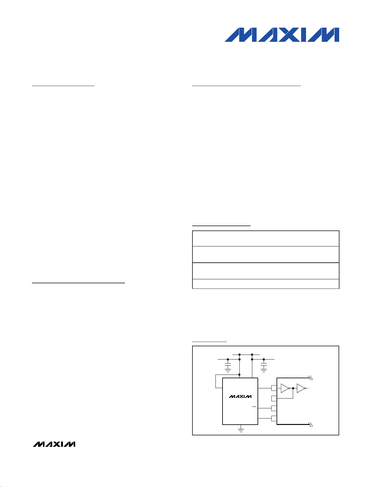
MAX7378
CLOCK
V
L
OSC1
OSC2
µCRST
I/O PORT
V
CC
SUPPLY VOLTAGE
ENABLE
RST/RST
SPEED
Typical Application Circuit
µMAX is a registered trademark of Maxim Integrated Products, Inc.
PART
TEMP RANGE
RESET
PIN-
PACKAGE
MAX7378A _ _ _
push-pull
8 µMAX
MAX7378B _ _ _
push-pull
8 µMAX
MAX7378C _ _ _
8 µMAX
Standard version is shown in bold. The first letter after the part
number designates the reset output option. Insert the letter corresponding to the desired reset threshold level from Table 1 in
the next position. Insert the two-letter code from Table 2 in the
remaining two positions for the desired frequency range. See
Table 3 for standard part numbers.
OUTPUT
-40oC to +125oC
-40oC to +125oC
-40oC to +125oC Open drain
Active high
Active low
Page 2
MAX7378
Silicon Oscillator with Low-Power
Frequency Switching and Reset Output
2 _______________________________________________________________________________________
ABSOLUTE MAXIMUM RATINGS
ELECTRICAL CHARACTERISTICS
(VCC= 2.7V to 5.5V, VL= VCC, TA= -40°C to +125°C, unless otherwise noted. Typical values are at VCC= 5V, TA = +25°C.) (Note 1)
Stresses beyond those listed under “Absolute Maximum Ratings” may cause permanent damage to the device. These are stress ratings only, and functional
operation of the device at these or any other conditions beyond those indicated in the operational sections of the specifications is not implied. Exposure to
absolute maximum rating conditions for extended periods may affect device reliability.
VCCto GND .............................................................-0.3V to +6V
All Other Pins to GND ................................-0.3V to (V
CC
+ 0.3V)
CLOCK Current ................................................................±10mA
Continuous Power Dissipation (T
A
= +70°C)
8-Pin µMAX (derate 4.5mW/°C above +70°C)....362mW (U8-1)
Operating Temperature Range .........................-40°C to +135°C
Junction Temperature .....................................................+150°C
Storage Temperature Range.............................-60°C to +150°C
Lead Temperature (soldering, 10s).................................+300°C
PARAMETER
CONDITIONS
UNITS
Operating Supply Voltage V
CC
2.7 5.5 V
Logic Output Supply Voltage V
L
Must be connected to V
CC
2.7 5.5 V
f
CLOCK
= 8MHz, no load 2.4 5.5 mA
Operating Supply Current
f
CLOCK
= 32.768kHz, no load 11 25 µA
Shutdown Current I
SHDN
ENABLE = 0V; ICC + I
L
3.0 7.5 µA
LOGIC INPUT (SPEED, ENABLE)
Input High Voltage V
IH
0.7 x
V
Input Low Voltage V
IL
0.3 x
V
Input Current I
IN
2µA
CLOCK OUTPUT
VL = 4.5V, I
SOURCE
= 9mA
V
L
-
0.4
Output High Voltage V
OH
VL = 2.7V, I
SOURCE
= 2.5mA
V
L
-
0.4
V
VL = 4.5V, I
SINK
= 20mA 0.4
Output Low Voltage V
OL
VL = 2.7V, I
SINK
= 10mA 0.4
V
VCC = 5V, TA = +25°C (Note 2) -2 +2
Initial Fast CLOCK Frequency
Accuracy
VCC = 2.7V to 5.5V, TA = +25°C -4 +4
%
Fast CLOCK Frequency
Temperature Sensitivity
(Note 3)
ppm/oC
VCC = 5V, TA = +25°C
Initial Slow CLOCK Frequency
Accuracy
VCC = 2.7V to 5.5V, TA = +25°C
kHz
Slow CLOCK Frequency
Temperature Sensitivity
(Note 3)
ppm/oC
SYMBOL
I
+ I
CC
I
+ I
CC
L
L
MIN TYP MAX
f
FCLOCK
f
SCLOCK
V
CC
32.440 32.768 33.096
31.785 33.751
±50 ±325
±50 ±325
V
CC
Page 3
MAX7378
Silicon Oscillator with Low-Power
Frequency Switching and Reset Output
_______________________________________________________________________________________ 3
Note 1: All parameters are tested at TA= +25°C. Specifications over temperature are guaranteed by design.
Note 2: The frequency is determined by part number selection. See the Ordering Information.
Note 3: Guaranteed by design. Not production tested.
ELECTRICAL CHARACTERISTICS (continued)
(VCC= 2.7V to 5.5V, VL= VCC, TA= -40°C to +125°C, unless otherwise noted. Typical values are at VCC= 5V, TA = +25°C.) (Note 1)
PARAMETER
SYMBOL
CONDITIONS
MIN
TYP
MAX
UNITS
CLOCK Output Duty Cycle 43 50 57 %
CLOCK Output Jitter
Observation of 8MHz output for 20s using a
500MHz oscilloscope
ps
P-P
CLOCK Output Rise Time t
R
10% to 90% 5 ns
CLOCK Output Fall Time t
F
90% to 10% 5 ns
RST/RST OUTPUT
TA = +25°C
V
TH
-
VTH +
Reset Threshold V
TH+
VCC rising
T
A
= -40°C to +125°C
V
TH
-
5%
VTH +
5%
V
Reset Hysteresis V
THYS
V
HYST
= {(V
TH+
) - ( V
TH-
)}/(V
TH-
) x 100% 2.0 %
POR Delay
µs
VL = 4.5V, I
SOURCE
= 9mA VL - 0.4
Output High Voltage V
OH
VL = 2.7V, I
SOURCE
= 2.5mA VL - 0.4
V
VL = 4.5V, I
SINK
= 20mA 0.4
Output Low Voltage V
OL
VL = 2.7V, I
SINK
= 10mA 0.4
V
160
1.5%
VCC rising from 0V to (VTH +200mV) in 1µs 100
1.5%
Page 4

Typical Operating Characteristics
(VCC= VL= 5V, TA = +25°C, unless otherwise noted.)
MAX7378
Silicon Oscillator with Low-Power
Frequency Switching and Reset Output
4 _______________________________________________________________________________________
DUTY CYCLE vs. TEMPERATURE
MAX7378 toc01
TEMPERATURE (°C)
DUTY CYCLE (%)
1209545 70-5 20-30
46
47
48
49
50
51
52
53
54
55
45
-55
CLOCK = 32kHz
DUTY CYCLE vs. TEMPERATURE
MAX7378 toc02
TEMPERATURE (°C)
DUTY CYCLE (%)
20-5-30
46
47
48
49
50
51
52
53
54
55
45
-55 45 70 95 120
CLOCK = 4MHz
DUTY CYCLE vs. SUPPLY VOLTAGE
MAX7378 toc03
SUPPLY VOLTAGE (V)
DUTY CYCLE (%)
5.24.94.6
46
47
48
49
50
51
52
53
54
55
45
4.3 5.5
CLOCK = 32kHz
DUTY CYCLE vs. SUPPLY VOLTAGE
MAX7378 toc04
SUPPLY VOLTAGE (V)
DUTY CYCLE (%)
5.24.94.6
46
47
48
49
50
51
52
53
54
55
45
4.3 5.5
CLOCK = 4MHz
SUPPLY CURRENT vs. TEMPERATURE
MAX7378 toc05
TEMPERATURE (°C)
SUPPLY CURRENT (µA)
1209545 70-5 20-30
10.0
10.5
11.0
11.5
12.0
12.5
13.0
13.5
14.0
-55
CLOCK = 32kHz
SUPPLY CURRENT vs. TEMPERATURE
MAX7378 toc06
TEMPERATURE (°C)
SUPPLY CURRENT (mA)
1209545 70-5 20-30
0.6
0.7
0.8
0.9
1.0
1.1
1.2
1.3
1.4
1.5
0.5
-55
CLOCK = 4 MHz
SUPPLY CURRENT vs. SUPPLY VOLTAGE
MAX7378 toc07
SUPPLY VOLTAGE (V)
SUPPLY CURRENT (µA)
5.24.94.6
8
9
10
11
12
13
14
4.3 5.5
CLOCK = 32kHz
SUPPLY CURRENT vs. SUPPLY VOLTAGE
MAX7378 toc08
SUPPLY VOLTAGE (V)
SUPPLY CURRENT (mA)
5.24.94.6
0.6
0.7
0.8
0.9
1.0
1.1
1.2
1.3
1.4
1.5
0.5
4.3 5.5
CLOCK = 4MHz
FREQUENCY vs. SUPPLY VOLTAGE
MAX7378 toc09
SUPPLY VOLTAGE (V)
FREQUENCY (kHz)
5.24.94.6
30.5
31.0
31.5
32.0
32.5
33.0
33.5
34.0
34.5
35.0
30.0
4.3 5.5
CLOCK = 32kHz
Page 5

MAX7378
Silicon Oscillator with Low-Power
Frequency Switching and Reset Output
_______________________________________________________________________________________ 5
FREQUENCY vs. SUPPLY VOLTAGE
MAX7378 toc10
SUPPLY VOLTAGE (V)
FREQUENCY (MHz)
5.24.94.6
3.92
3.94
3.96
3.98
4.00
4.02
4.04
4.06
4.08
4.10
3.90
4.3 5.5
CLOCK = 4MHz
FREQUENCY vs. TEMPERATURE
MAX7378 toc11
TEMPERATURE (°C)
FREQUENCY (kHz)
1209545 70-5 20-30
32.1
32.2
32.3
32.4
32.5
32.6
32.7
32.8
32.9
33.0
32.0
-55
CLOCK = 32kHz
FREQUENCY vs. TEMPERATURE
MAX7378 toc12
TEMPERATURE (°C)
FREQUENCY (MHz)
1209545 70-5 20-30
3.92
3.94
3.96
3.98
4.00
4.02
4.04
4.06
4.08
4.10
3.90
-55
CLOCK = 4MHz
CLOCK OUTPUT WAVEFORM (CL = 10pF)
MAX7378 toc13
40ns/div
F = 4MHz, CL = 10pF
CLOCK OUTPUT WAVEFORM (CL = 50pF)
MAX7378 toc14
40ns/div
F = 4MHz, CL = 50pF
CLOCK OUTPUT WAVEFORM (CL = 100pF)
MAX7378 toc15
40ns/div
F = 4MHz, CL = 100pF
MAXIMUM TRANSIENT DURATION
vs. RESET THRESHOLD
MAX7378 toc16
RESET THRESHOLD OVERDRIVE (mV)
MAXIMUM TRANSIENT DURATION (µs)
200 400 600 800
100
1000
10
01000
RESET = 4.29V
RESET OCCURS
ABOVE THE CURVE
HIGH-SPEED TO LOW-SPEED
TRANSITION
MAX7378 toc17
CLOCK
SPEED
20µs/div
HIGH-SPEED TO LOW-SPEED
TRANSITION (EXPANDED SCALE)
MAX7378 toc18
CLOCK
SPEED
400µs/div
Typical Operating Characteristics (continued)
(VCC= VL= 5V, TA = +25°C, unless otherwise noted.)
Page 6

MAX7378
Silicon Oscillator with Low-Power
Frequency Switching and Reset Output
6 _______________________________________________________________________________________
Detailed Description
The MAX7378 is a dual-speed clock generator with
integrated reset for microcontrollers and UARTs in 3V,
3.3V, and 5V applications (Figure 1). The MAX7378 is a
replacement for two crystal-oscillator modules, crystals,
or ceramic resonators and a system-reset IC. The highspeed clock frequency is factory trimmed to specific
values. A variety of popular standard frequencies are
available (Table 2). The low-speed clock frequency is
fixed at 32.768kHz (Figure 1). No external components
are required for setting or adjusting the frequency.
Supply Voltage
The MAX7378 has been designed for use in systems
with nominal supply voltages of 3V, 3.3V, or 5V and is
specified for operation with supply voltages in the 2.7V
to 5.5V range. See the Absolute Maximum Ratings section for limit values of power-supply and pin voltages.
Oscillator
The clock output is a push-pull configuration and is
capable of driving a ground-connected 500Ω or a positive-supply connected 250Ω load to within 400mV of
either supply rail. The clock output remains stable over
the full operating voltage range and does not generate
short output cycles when switching between high- and
low-speed modes. A typical startup characteristic is
shown in the Typical Operating Characteristics.
Pin Description
PIN NAME FUNCTION
1VCCPositive Supply Voltage. Bypass VCC to GND with a 0.1µF capacitor.
2VLOutput Supply Voltage. Connect VL to VCC. Bypass VL to GND with a 0.1µF capacitor.
3 SPEED
Clock Speed-Select Input. Drive SPEED low to select the 32kHz fixed frequency. Drive SPEED high to
select factory-trimmed frequency.
4 RST Reset Output. See the RST Reset Output Options section for more details.
5 CLOCK Push-Pull Clock Output
6 GND Ground
7 ENABLE Active-High Clock Enable Input. See the ENABLE Input section for more details.
8N. C. No Connect. No internal connection.
Typical Operating Characteristics (continued)
(VCC= VL= 5V, TA = +25°C, unless otherwise noted.)
LOW-SPEED TO HIGH-SPEED
TRANSITION
MAX7378 toc19
LOW-SPEED TO HIGH-SPEED TRANSITION
(EXPANDED SCALE)
MAX7378 toc20
20µs/div
CLOCK
SPEED
CLOCK
SPEED
400µs/div
Page 7

MAX7378
Silicon Oscillator with Low-Power
Frequency Switching and Reset Output
_______________________________________________________________________________________ 7
ENABLE Input
The MAX7378 has an active-high enable input that controls the clock and reset outputs. The clock output is
driven high when disabled. The reset asserts when disabled (low for active-low reset, high for active-high
reset). Drive ENABLE low to disable the clock output on
the next rising edge. Drive ENABLE high to activate the
clock output.
Clock-Speed Select Input
The MAX7378 uses logic input pin, SPEED, to set clock
speed. Take this pin low to select slow clock speed
(nominally 32.768kHz) or high to select full clock
speed. The SPEED input may be strapped to VCCor to
GND to select fast or slow clock speed, or connected
to a logic output (such as a processor port) used to
change clock speed on the fly. If the SPEED input is
connected to a processor port that powers up in the
input condition, connect a pullup or pulldown resistor to
the SPEED input to set the clock to the preferred speed
on power-up. The leakage current through the resistor
into the SPEED input is very low, so a resistor value as
high as 500kΩ may be used.
Applications Information
Interfacing to a Microcontroller
Clock Input
The MAX7378 clock output is a push-pull, CMOS logic
output that directly drives any µP or µC clock input.
There are no impedance-matching issues when using
the MAX7378. The MAX7378 is not sensitive to its position on the board and does not need to be placed right
next to the µP. Connect the MAX7378 VLpin and µC (or
other clock-input device) to the same supply voltage
level. Refer to the µC data sheet for clock-input compatibility with external clock signals. The MAX7378 requires
no biasing components or load capacitance. When
using the MAX7378 to retrofit a crystal oscillator, remove
all biasing components from the oscillator input.
RST Reset Output Options
The MAX7378 is available with three reset output stage
options: push-pull with active-low output, push-pull with
active-high output, and open drain with active-low output. The RST output is asserted when the monitored
input (VCC) drops below the internal V
TH-
threshold and
remains asserted for 100µs after the monitored input
exceeds the internal V
TH+
threshold. The open-drain
RST output requires an external pullup resistor.
Output Jitter
The MAX7378’s jitter performance is given in the
Electrical Characteristics table as a peak-to-peak value
obtained by observing the output of the MAX7378 for
20s with a 500MHz oscilloscope. Jitter values are
approximately proportional to the period of the output
frequency of the device. Thus, a 4MHz part has
approximately twice the jitter value of an 8MHz part.
The jitter performance of clock sources degrades in the
presence of mechanical and electrical interference.
The MAX7378 is relatively immune to vibration, shock,
and EMI influences, and thus provides a considerably
more robust clock source than crystal or ceramic resonator-based oscillator circuits.
Initial Power-Up and Operation
An intial power-up reset holds the reset output active for
100µs (typ). However, the clock starts up within 30µs
(typ) at the frequency determined by the SPEED pin.
Power-Supply Brownout
The RST output is asserted whenever VCCdrops below
the specified threshold level. The action of VCCdropping below the reset threshold and then rising back
above the threshold asserts RST and starts a normal
RST/RST
LOGIC
600kHz TO 10MHz
(HF OSCILLATOR)
POR
MUX
CLOCK
SPEED
ENABLE
V
CC
V
L
MAX7378
32kHz
(LF OSCILLATOR)
Figure 1. Functional Diagram
Page 8

MAX7378
power-on reset cycle. The MAX7378 reset circuit features internal hysteresis that creates two trip points: one
for rising supply voltage and one for falling supply voltage. The standard threshold values (see Table 1) are
the trip points for rising supply voltage. The trip point
for falling supply voltage is calculated by subtracting
the hysteresis value from the rising supply trip point.
The hysteresis prevents the reset output from oscillating (chattering) when VCCis near the voltage threshold.
The reset circuit is immune to short transient VCCdrops
(see Maximum Transient Duration vs. Reset Threshold
in the Typical Operating Characteristics).
Extended Temperature Operation
The MAX7378 was tested to +135°C during product
characterization and shown to function normally at
this temperature (see the Typical Operating Characteris-
tics). However, production test and qualification is only
performed from -40°C to +125°C at this time. Contact the
factory if operation outside this range is required.
Power-Supply Considerations
The MAX7378 operates with a 2.7V and 5.5V powersupply voltage. There are two power-supply pins, V
CC
and VL. VCCprovides the main power input to the
device and VLsupplies the clock and reset output circuits. Good power-supply decoupling is needed to
maintain the power-supply rejection performance of the
MAX7378. Bypass both VCCand VLto GND with a
0.1µF surface-mount ceramic capacitor. Mount the
bypassing capacitors as close to the device as possible. If possible, mount the MAX7378 close to the µC’s
decoupling capacitor so that additional decoupling is
not required. A larger value bypass capacitor is recommended if the MAX7378 is to operate with a large
capacitive load. Use a bypass capacitor value of at
least 1000 times that of the output load capacitance.
Note: VLmust be equal to VCC.
Silicon Oscillator with Low-Power
Frequency Switching and Reset Output
8 _______________________________________________________________________________________
Pin Configuration
TOP VIEW
1
2
3
4
8
7
6
5
N.C.
ENABLE
GND
CLOCKRST
SPEED
V
L
V
CC
MAX7378
µMAX
Table 1. Standard Reset Threshold Levels
Table 2. Standard Frequencies
For all other reset threshold options, contact the factory.
For all other frequency options, contact the factory.
SUFFIX RESET THRESHOLD (V)
R 2.57
M 4.29
SUFFIX STANDARD FREQUENCY (MHz)
MG 1
OK 1.8432
QT 3.39545
QW 3.6864
RD 4
RH 4.1943
TP 8
Page 9

MAX7378
Silicon Oscillator with Low-Power
Frequency Switching and Reset Output
_______________________________________________________________________________________ 9
PART PIN-PACKAGE
FREQUENCY (MHZ)
MAX7378CRMG 8 µMAX Open drain 2.57 1
MAX7378CROK 8 µMAX Open drain 2.57 1.8432
MAX7378CRQT 8 µMAX Open drain 2.57 3.39545
MAX7378CRQW 8 µMAX Open drain 2.57 3.6864
MAX7378CRRD 8 µMAX Open drain 2.57 4
MAX7378CRRH 8 µMAX Open drain 2.57 4.1943
MAX7378CRTP 8 µMAX Open drain 2.57 8
MAX7378CMMG 8 µMAX Open drain 4.29 1
MAX7378CMOK 8 µMAX Open drain 4.29 1.8432
MAX7378CMQT 8 µMAX Open drain 4.29 3.39545
MAX7378CMQW
8 µMAX Open drain 4.29 3.6864
MAX7378CMRD 8 µMAX Open drain 4.29 4
MAX7378CMRH 8 µMAX Open drain 4.29 4.1943
MAX7378CMTP 8 µMAX Open drain 4.29 8
Table 3. Standard Part Numbers
Chip Information
TRANSISTOR COUNT: 2027
PROCESS: BiCMOS
RESET OUTPUT TYPE R ESET T H R ESH O L D ( V)
Page 10

MAX7378
Silicon Oscillator with Low-Power
Frequency Switching and Reset Output
Maxim cannot assume responsibility for use of any circuitry other than circuitry entirely embodied in a Maxim product. No circuit patent licenses are
implied. Maxim reserves the right to change the circuitry and specifications without notice at any time.
10 ____________________Maxim Integrated Products, 120 San Gabriel Drive, Sunnyvale, CA 94086 408-737-7600
© 2004 Maxim Integrated Products Printed USA is a registered trademark of Maxim Integrated Products.
Package Information
(The package drawing(s) in this data sheet may not reflect the most current specifications. For the latest package outline information
go to www.maxim-ic.com/packages
.)
8LUMAXD.EPS
PACKAGE OUTLINE, 8L uMAX/uSOP
1
1
21-0036
J
REV.DOCUMENT CONTROL NO.APPROVAL
PROPRIETARY INFORMATION
TITLE:
MAX
0.043
0.006
0.014
0.120
0.120
0.198
0.026
0.007
0.037
0.0207 BSC
0.0256 BSC
A2
A1
c
e
b
A
L
FRONT VIEW
SIDE VIEW
E H
0.6±0.1
0.6±0.1
ÿ 0.50±0.1
1
TOP VIEW
D
8
A2
0.030
BOTTOM VIEW
1
6∞
S
b
L
H
E
D
e
c
0∞
0.010
0.116
0.116
0.188
0.016
0.005
8
4X S
INCHES
-
A1
A
MIN
0.002
0.950.75
0.5250 BSC
0.25 0.36
2.95 3.05
2.95 3.05
4.78
0.41
0.65 BSC
5.03
0.66
6∞0∞
0.13 0.18
MAX
MIN
MILLIMETERS
- 1.10
0.05 0.15
α
α
DIM
 Loading...