

Page 1
现货库存、技术资料、百科信息、热点资讯,精彩尽在鼎好!
General Description
The MAX7376 silicon oscillator with reset, is a replacement for ceramic resonators, crystals, crystal oscillator
modules, and discrete reset circuits. The MAX7376 provides the primary clock source and reset function for
microcontrollers in 3V, 3.3V, and 5V applications. The
MAX7376 features a factory-programmed high-speed
oscillator and a microprocessor (µP) power-on-reset
(POR) supervisor.
Unlike typical crystal and ceramic resonator oscillator
circuits, the MAX7376 is resistant to vibration and EMI.
The high-output-drive current and absence of highimpedance nodes make the oscillator less susceptible
to dirty or humid operating conditions. With a wide
operating temperature range as standard, the MAX7376
is a good choice for demanding home appliance,
industrial, and automotive environments.
The MAX7376 is available in factory-programmed frequencies from 32.768kHz to 10MHz. See Table 2 for
standard frequencies and contact the factory for custom frequencies.
The MAX7376 is available in a 5-pin SOT23 package.
Refer to the MAX7382 data sheet for frequencies
≥10MHz. The MAX7376 standard operating temperature range is -40°C to +125°C. See the Applications
Information section for the extended operating temperature range.
Applications
White Goods
Automotive
Consumer Products
Appliances and Controls
Handheld Products
Portable Equipment
Microcontroller (µC) Systems
Features
♦ 2.7V to 5.5V Operation
♦ Accurate Oscillator: 600kHz to 10MHz or 32kHz
♦ Reset Output Holds the µC in Reset for 100µs
After Clock Startup
♦ ±10mA Clock Output Drive Capability
♦ 2% Initial Accuracy
♦ ±50ppm/°C Temperature Coefficient
♦ 50% Duty Cycle
♦ 5ns Output Rise and Fall Time
♦ Low Jitter: 160ps
P-P
)
at 8MHz (No PLL)
♦ 3mA Operating Current (8MHz)
♦ 13µA Operating Current (32kHz)
♦ -40°C to +125°C Temperature Range
MAX7376
Silicon Oscillator with Reset Output
________________________________________________________________ Maxim Integrated Products 1
Pin Configuration
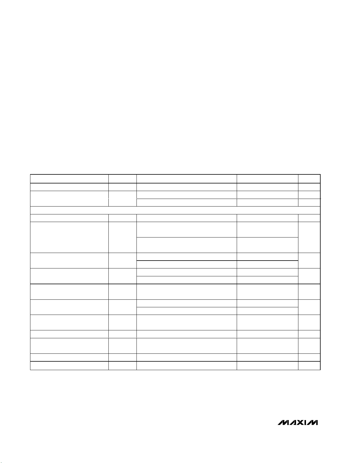
Ordering Information
19-3475; Rev 0; 10/04
For pricing, delivery, and ordering information, please contact Maxim/Dallas Direct! at
1-888-629-4642, or visit Maxim’s website at www.maxim-ic.com.
Standard version is shown in bold.
The first letter after the part number designates the reset output
option. Insert the letter corresponding to the desired reset
threshold level from Table 1 in the next position. Insert the twoletter code from Table 2 in the remaining two positions for the
desired frequency range. See Table 3 for standard part numbers.
Typical Application Circuit appears at end of data sheet.
PART TEMP RANGE
M A X7 3 7 6C _ _ _ - T -40°C to +125°C5 SOT23-5 Open drain
M AX7376A_ _ _- T -40°C to +125°C5 SOT23-5
M AX7376B_ _ _- T -40°C to +125°C5 SOT23-5
PINPACKAGE
RESET
OUTPUT
Active high
push-pull
Active low
push-pull
TOP VIEW
15E.C.CLOCK
MAX7376
2
GND
3
RST/RST
SOT23
4
V
CC
Page 2
MAX7376
Silicon Oscillator with Reset Output
2 _______________________________________________________________________________________
ABSOLUTE MAXIMUM RATINGS
ELECTRICAL CHARACTERISTICS
(VCC= 2.7V to 5.5V, TA= -40°C to +125°C, unless otherwise noted. Typical values are at VCC= 5V and TA = +25°C.) (Note 1)
Stresses beyond those listed under “Absolute Maximum Ratings” may cause permanent damage to the device. These are stress ratings only, and functional
operation of the device at these or any other conditions beyond those indicated in the operational sections of the specifications is not implied. Exposure to
absolute maximum rating conditions for extended periods may affect device reliability.
VCCto GND .............................................................-0.3V to +6V
All Other Pins to GND ................................-0.3V to (V
CC
+ 0.3V)
CLOCK Current ................................................................±10mA
Continuous Power Dissipation (T
A
= +70°C)
5-Pin SOT23
(derate 7.1mW/°C above +70°C) ...................571mW (U5 - 2)
Operating Temperature Range.........................-40°C to +135°C
Junction Temperature .....................................................+150°C
Storage Temperature Range.............................-60°C to +150°C
Lead Temperature (soldering, 10s).................................+300°C
Operating Supply Voltage V
Operating Supply Current I
CLOCK OUTPUT
Minimum Operating Voltage 1.65 V
Output High Voltage V
Output Low Voltage V
Initial Frequency Accuracy f
Frequency Temperature
Sensitivity
Initial Frequency Accuracy
(32.768kHz)
Frequency Temperature
Sensitivity
CLOCK Output Duty Cycle 43 50 57 %
CLOCK Output Jitter
CLOCK Output Rise Time t
CLOCK Output Fall Time t
PARAMETER SYMBOL CONDITIONS MIN TYP MAX UNITS
CC
f
= 8MHz, no load 3 5 mA
CC
CLOCK
f
= 32.768kHz, no load 13 25 µA
CLOCK
VCC = 4.5V, I
OH
VCC = 2.7V, I
VCC = 4.5V, I
OL
VCC = 2.7V, I
CLOCK
VCC = 5V, TA = +25°C (Note 2) -2 +2
VCC = 2.7V to 5.5V, TA = +25°C -4 +4
(Note 3) ±50 ±325 ppm/
f
CLOCK
VCC = 5V, TA = +25°C (Note 2) 32.440 32.768 33.096
VCC = 2.7V to 5.5V, TA = +25°C 31.785 33.751
32.768kHz (Note 3) ±50 ±325 ppm/
Observation of 8MHz output for 20s using a
500MHz oscilloscope
10% to 90% 5 ns
R
90% to 10% 5 ns
F
2.7 5.5 V
V
= 9mA
SOURCE
= 2.5mA
SOURCE
= 20mA 0.4
SINK
= 10mA 0.4
SINK
CC
- 0.4
V
CC
- 0.4
160 ps
V
V
%
kHz
o
C
o
C
-
Page 3
MAX7376
Silicon Oscillator with Reset Output
_______________________________________________________________________________________ 3
Note 1: All parameters are tested at TA= +25°C. Specifications over temperature are guaranteed by design.
Note 2: The frequency is determined by part number selection. See Table 3.
Note 3: Guaranteed by design. Not production tested.
ELECTRICAL CHARACTERISTICS (continued)
(VCC= 2.7V to 5.5V, TA= -40°C to +125°C, unless otherwise noted. Typical values are at VCC= 5V and TA = +25°C.) (Note 1)
Typical Operating Characteristics
(VCC= 5V, TA= +25°C, unless otherwise noted.)
RST/RST OUTPUT
Reset Threshold V
Reset Hysteresis V
POR Delay VCC rising from 0V to (VTH + 200mV) in 1µs 100 µs
Output High Voltage V
Output Low Voltage V
Leakage Current I
PARAMETER SYMBOL CONDITIONS MIN TYP MAX UNITS
V
TH+
THYS
OH
OL
LEAK
VCC rising
V
= {(V
HYST
TH+
VCC = 4.5V, I
VCC = 2.7V, I
VCC = 4.5V, I
VCC = 2.7V, I
VCC = 5.5V, V
-
V
TH
2%
TH
5%
-
TA = +25°C
T
= -40°C to +125°C
A
) - ( V
SOURCE
SOURCE
SINK
SINK
RST
)}/(V
TH-
) x 100% 2.0 %
TH-
= 9mA VCC - 0.4
= 2.5mA VCC - 0.4
= 20mA 0.4
= 10mA 0.4
= 5.5V, open drain 1 µA
VTH +
2%
VTH +
5%
V
V
V
DUTY CYCLE
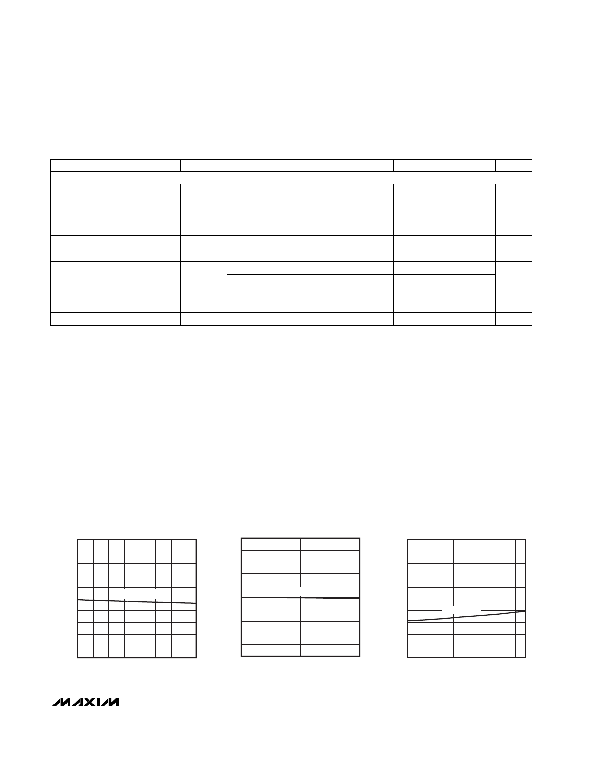
vs. TEMPERATURE
55
54
53
52
51
50
49
DUTY CYCLE (%)
48
47
46
45
-55 -5 20 45 70-30 95 120
CLOCK = 4MHz
TEMPERATURE (°C)
MAX7376 toc01
DUTY CYCLE (%)
DUTY CYCLE
vs. SUPPLY VOLTAGE
55
54
53
52
51
50
49
48
47
46
45
4.3 4.6 4.9 5.2 5.5
CLOCK = 4MHz
SUPPLY VOLTAGE (V)
MAX7376 toc02
SUPPLY CURRENT (mA)
SUPPLY CURRENT
vs. TEMPERATURE
1.5
1.4
1.3
1.2
1.1
1.0
0.9
0.8
0.7
0.6
0.5
-55 -5 20 45 70-30 95 120
CLOCK = 4MHz
TEMPERATURE (°C)
MAX7376 toc03
Page 4
MAX7376
Silicon Oscillator with Reset Output
4 _______________________________________________________________________________________
Typical Operating Characteristics (continued)
(VCC= 5V, TA= +25°C, unless otherwise noted.)
SUPPLY CURRENT
vs. SUPPLY VOLTAGE
1.5
1.4
1.3
1.2
1.1
1.0
0.9
CLOCK = 4MHz
0.8
SUPPLY CURRENT (mA)
0.7
0.6
0.5
4.3 4.6 4.9 5.2 5.5
SUPPLY VOLTAGE (V)
MAX7376 toc04
FREQUENCY (MHz)
4.10
4.08
4.06
4.04
4.02
4.00
3.98
3.96
3.94
3.92
3.90
4.3 4.6 4.9 5.2 5.5
FREQUENCY
vs. SUPPLY VOLTAGE
MAX7376 toc05
CLOCK = 4MHz
SUPPLY VOLTAGE (V)
FREQUENCY
vs. TEMPERATURE
4.10
4.08
4.06
4.04
4.02
4.00
3.98
FREQUENCY (MHz)
3.96
3.94
3.92
3.90
-55 -5 20 45 70-30 95 120
CLOCK = 4MHz
TEMPERATURE (°C)
MAX7376 toc06
CLOCK OUTPUT WAVEFORM
= 10pF)
(C
L
f = 4MHz, CL = 10pF
40ns/div
MAX7376 toc07
CLOCK
s)
µ
CLOCK OUTPUT WAVEFORM
(C
f = 4MHz, CL = 50pF
MAXIMUM TRANSIENT DURATION
vs. RESET THRESHOLD
1000
RESET OCCURS
ABOVE THE CURVE
100
= 50pF)
L
40ns/div
MAX7376 toc08
CLOCK
MAX7376 toc10
CLOCK OUTPUT WAVEFORM
= 100pF)
(C
L
f = 4MHz, CL = 100pF
40ns/div
MAX7376 toc09
CLOCK
MAXIMUM TRANSIENT DURATION (
10
0 200 400 600 800 1000
RESET THRESHOLD OVERDRIVE (mV)
RESET = 4.29V
Page 5
MAX7376
Silicon Oscillator with Reset Output
_______________________________________________________________________________________ 5
Detailed Description
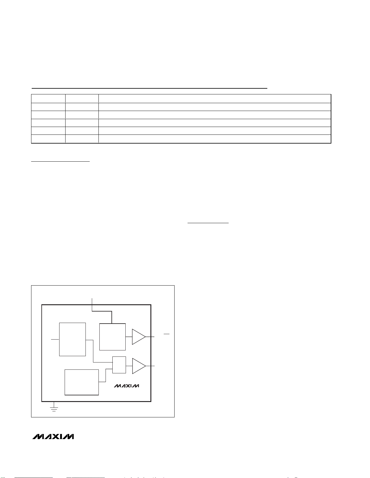
The MAX7376 is a clock generator with integrated reset
for µCs and UARTs in 3V, 3.3V, and 5V applications
(Figure 1). The MAX7376 is a replacement for crystal
oscillator modules, crystals, or ceramic resonators and
a system-reset IC. The clock frequency is factory
trimmed to specific values. A variety of popular standard frequencies are available (Table 2). No external
components are required for setting or adjusting the
frequency.
Supply Voltage
The MAX7376 has been designed for use in systems
with nominal supply voltages of 3V, 3.3V, or 5V and is
specified for operation with supply voltages in the 2.7V
to 5.5V range. See the Absolute Maximum Ratings section for limit values of power-supply and pin voltages.
Oscillator
The clock output is a push-pull configuration and is
capable of driving a ground-connected 500Ω or a positive-supply-connected 250Ω load to within 400mV of
either supply rail. The clock output remains stable over
the full operating voltage range and does not generate
short output cycles during either power-on or power-off.
A typical startup characteristic is shown in the Typical
Operating Characteristics.
Applications Information
Interfacing to a µC Clock Input
The MAX7376 clock output is a push-pull, CMOS, logic
output that directly drives any µP or µC clock input.
There are no impedance-matching issues when using
the MAX7376. The MAX7376 is not sensitive to its position on the board and it does not need to be placed right
next to the µP. Refer to the µC data sheet for clock-input
compatibility with external clock signals. The MAX7376
requires no biasing components or load capacitance.
When using the MAX7376 to retrofit a crystal oscillator,
remove all biasing components from the oscillator input.
RST Reset Output Options
The MAX7376 is available with three reset output stage
options: push-pull with active-low output, push-pull with
active-high output, and open drain with active-low output. The RST output is asserted when the monitored
input (VCC) drops below the internal V
TH-
threshold and
remains asserted for 100µs after the monitored input
exceeds the internal V
TH+
threshold. The open-drain
RST output requires an external pullup resistor.
Output Jitter
The MAX7376’s jitter performance is given in the
Electrical Characteristics table as a peak-to-peak value
obtained by observing the output of the MAX7376 for
20s with a 500MHz oscilloscope. Jitter values are
approximately proportional to the period of the output
frequency of the device. Thus, a 4MHz part has
approximately twice the jitter value of an 8MHz part.
The jitter performance of clock sources degrades in the
presence of mechanical and electrical interference.
Pin Description
Figure 1. Functional Diagram
PIN NAME FUNCTION
1 CLOCK Push-Pull Clock Output
2 GND Ground
3 RST Reset Output. See the RST Reset Output Options section for more details.
4VCCPositive Supply Voltage. Bypass VCC to GND with a 0.1µF capacitor.
5 E.C. Must Be Externally Connected to V
CC
V
CC
BIAS_V
LOGIC
600kHz TO 10MHz
POR
MUX
MAX7376
RST/RST
CLOCK
Page 6

MAX7376
Silicon Oscillator with Reset Output
6 _______________________________________________________________________________________
Typical Application Circuit
The MAX7376 is relatively immune to vibration, shock,
and EMI influences, and thus provides a considerably
more robust clock source than crystal or ceramic resonator-based oscillator circuits.
Initial Power-Up and Operation
The clock starts up within 30µs (typ) after VCChas risen
above the reset threshold. The reset output remains
asserted for 100µs after the reset threshold is reached.
Extended Temperature Operation
The MAX7376 was tested to +135°C during product
characterization and shown to function normally at
this temperature (see the Typical Operating
Characteristics). However, production test and qualification is only performed from -40°C to +125°C at this
time. Contact the factory if operation outside this range
is required.
Power-Supply Considerations
The MAX7376 operates with a 2.7V and 5.5V powersupply voltage. Good power-supply decoupling is
needed to maintain the power-supply rejection performance of the MAX7376. Bypass VCCto GND with a
0.1µF surface-mount ceramic capacitor. Mount the
bypass capacitor as close to the device as possible. If
possible, mount the MAX7376 close to the µC’s decoupling capacitor so that additional decoupling is not
required. A larger value bypass capacitor is recommended if the MAX7376 is to operate with a large
capacitive load. Use a bypass capacitor value of at
least 1000 times that of the output load capacitance.
Table 1. Standard Reset Threshold Levels
Table 2. Standard Frequencies
For all other reset threshold options, contact factory.
For all other reset threshold options, contact factory.
SUFFIX RESET THRESHOLD (V)
R 2.57
M 4.29
SUPPLY VOLTAGE
V
CC
SUFFIX STANDARD FREQUENCY (MHz)
AA 32.768kHz
MG 1
OK 1.8432
QT 3.39545
QW 3.6864
RD 4
RH 4.1943
TP 8
E.C.
MAX7376
CLOCK
RST/RST
OSC1
OSC2
µCRST
Page 7

MAX7376
Silicon Oscillator with Reset Output
_______________________________________________________________________________________ 7
Chip Information
TRANSISTOR COUNT: 2027
PROCESS: BiCMOS
Table 3. Standard Part Numbers
PART PIN-PACKAGE
MAX7376CRAA 5 SOT23 2.57 32.768k AEUZ
MAX7376CRMG 5 SOT23 2.57 1M AEUN
MAX7376CROK 5 SOT23 2.57 1.8432M AEUJ
MAX7376CRQT 5 SOT23 2.57 3.39545M AETT
MAX7376CRQW 5 SOT23 2.57 3.6864M AETU
MAX7376CRRD 5 SOT23 2.57 4M AETV
MAX7376CRRH 5 SOT23 2.57 4.1943M AETW
MAX7376CRTP 5 SOT23 2.57 8M AESF
MAX7376CMMG 5 SOT23 4.29 1M AEUM
MAX7376CMOK 5 SOT23 4.29 1.8432M AEUI
MAX7376CMQT 5 SOT23 4.29 3.39545M AESH
MAX7376CMQW 5 SOT23 4.29 3.6864M AETP
MAX7376CMRD 5 SOT23 4.29 4M AESJ
MAX7376CMRH 5 SOT23 4.29 4.1943M AETR
MAX7376CMTP 5 SOT23 4.29 8M AETS
RESET THRESHOLD
(V)
FREQUENCY
(Hz)
TOP MARK
Page 8

MAX7376
Silicon Oscillator with Reset Output
Maxim cannot assume responsibility for use of any circuitry other than circuitry entirely embodied in a Maxim product. No circuit patent licenses are
implied. Maxim reserves the right to change the circuitry and specifications without notice at any time.
8 _____________________Maxim Integrated Products, 120 San Gabriel Drive, Sunnyvale, CA 94086 408-737-7600
© 2004 Maxim Integrated Products Printed USA is a registered trademark of Maxim Integrated Products.
Package Information
(The package drawing(s) in this data sheet may not reflect the most current specifications. For the latest package outline information
go to www.maxim-ic.com/packages
.)
PACKAGEOUTLINE,SOT-23,5L
21-0057
SOT-23 5L .EPS
1
E
1
 Loading...