

19-6036; Rev 0; 9/11
MAX7365
2
1MHz I
C-Interfaced 8 x 7
Key-Switch Controller with GPIO Ports
General Description
The MAX7365 is an I2C-interfaced peripheral that provides microprocessors with management of up to 56 key
switches.
Key codes generated for each keypress and release
enable easier implementation of multiple key entries. Key
inputs monitored statically, not dynamically, ensure lowEMI operation. The switches can be metallic or resistive
(carbon) with up to 5kI of resistance.
The device features autosleep and autowake to further
minimize the power consumption of the device. The
autosleep feature puts the device in a low-power state
(1FA typ) after a programmable sleep timeout period.
The autowake feature configures the device to return to
normal operating mode from sleep upon a keypress.
The key controller debounces and maintains a FIFO of keypress and release events (including autorepeat, if enabled).
An interrupt (INT) output can be configured to alert key-
presses either as they occur or at the maximum rate.
Unused key switches can be used as GPI. In addition,
there are five additional general-purpose input/output
(GPIO) ports. GPOs can be programmed as push-pull
or open-drain to high- or low-side output drivers. When
programmed as open drain, an optional on-chip 100kI
pullup/pulldown resister can be enabled.
The device is available in a small (2mm x 2mm) 25-bump
wafer-level package (WLP) for cell phones, pocket PCs,
and other portable consumer electronic applications.
The device operates over the -40NC to +85NC extended
temperature range.
Benefits and Features
S Reduce Processor Load
Monitor Up to 56 Keys
FIFO Queues Up to 16 Debounced Key Events
Hardware Interrupt at the FIFO Level or at the
End-of-Definable Time Period
S Increased Battery Life
Autosleep and Autowake Minimize Current
Consumption
Less Than 1µA Sleep Current
S Save Board Space
Small (2mm x 2mm) and Low-Profile 25-Bump
WLP
S Flexible Design Requirements
1.62V to 3.6V Operation
Proprietary Ghost-Key Detection and Removal
Key Debounce Time User Configurable from
1ms to 31ms
Low-EMI Design Uses Static Matrix Monitoring
Five Additional GPIO Ports
All Key Switches Can Be Used as GPIs
1Mbps, 5.5V Tolerant, Two-Wire Serial Interface
Selectable Two-Wire, Serial-Bus Timeout
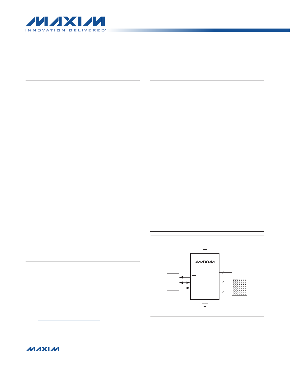
Typical Operating Circuit
+1.8V
V
MAX7365
INT
SDA
SCL
DD
GND
GPIO[0:4]
ROW[0:7]
COL[0:6]
5
I/O
8
7
56 KEYS
Applications
Netbooks
Cell Phones
PDAs
Handheld Games
Portable Consumer Electronics
Ordering Information appears at end of data sheet.
For related parts and recommended products to use with this part,
refer to www.maxim-ic.com/MAX7365.related.
����������������������������������������������������������������� Maxim Integrated Products 1
MCU
For pricing, delivery, and ordering information, please contact Maxim Direct at 1-888-629-4642,
or visit Maxim’s website at www.maxim-ic.com.
MAX7365
2
1MHz I
C-Interfaced 8 x 7
Key-Switch Controller with GPIO Ports
ABSOLUTE MAXIMUM RATINGS
VDD to GND ............................................................ -0.3V to 4.0V
ROW7–ROW0, COL6–COL0,
GPIO4–GPIO0 to GND
SDA, SCL, INT to GND
DC Current on ROW7–ROW0, COL6–COL0 to GND
DC Current on GPIO4–GPIO0 to GND
GND Current
Stresses beyond those listed under “Absolute Maximum Ratings” may cause permanent damage to the device. These are stress ratings only, and functional operation of the device at these or any other conditions beyond those indicated in the operational sections of the specifications is not implied. Exposure to absolute
maximum rating conditions for extended periods may affect device reliability.
......................................................................12mA
......................... -0.3V to (VDD + 0.3V)
.............................................. -0.3V to 6V
...........1mA
..............................12mA
PACKAGE THERMAL CHARACTERISTICS (Note 1)
Junction-to-Ambient Thermal Resistance (θ
Note 1: Package thermal resistances were obtained using the method described in JEDEC specification JESD51-7, using a four-
layer board. For detailed information on package thermal considerations, refer to www.maxim-ic.com/thermal-tutorial.
) ..............52NC/W
JA
ELECTRICAL CHARACTERISTICS
(VDD = 1.62V to 3.6V, TA = -40NC to +85NC, unless otherwise noted. Typical values are at VDD = 3.3V, TA = +25NC.) (Notes 2, 3)
PARAMETER SYMBOL CONDITIONS MIN TYP MAX UNITS
Operating Supply Voltage V
Operating Supply Current I
Sleep-Mode Supply Current I
Key-Switch Source Current I
Key-Switch Source Voltage V
Key-Switch Resistance R
Startup Time from Shutdown t
Keyscan Frequency f
Maximum Allowable Load
Capacitance for Keyscan Function
GPIO SPECIFICATIONS
Input High Voltage
GPIO_, ROW_, COL_, SDA, SCL
Input Low Voltage
GPIO_, ROW_, COL_, SDA, SCL
Input Leakage Current
GPIO_, ROW_, COL_, SDA, SCL
Output Logic Low Voltage
INT, SDA
Output Low Voltage
GPIO_
DD
DD
SL
KEY
KEY
KEY
START
KEY
V
IH
V
IL
I
IN
V
OL
N keys pressed; GPI static 34 + (25 x N)
All 56 key switches open 60 85
(Note 4) 5
N keys pressed simultaneously (Note 4) 500 pF
Input voltage = VDD or V
I
= 6mA 0.5 V
SINK
VDD = 1.8V and I
V
= 1.8V and I
DD
Continuous Power Dissipation (T
WLP (derate 19.2mW/NC above +70NC)....................1536mW
Operating Temperature Range
Junction Temperature
Storage Temperature Range
Soldering Temperature (reflow)
GND
= 5mA 40 100
SINK
= 10mA 80 200
SINK
.....................................................+150NC
= +70NC)
A
.......................... -40NC to +85NC
............................ -65NC to +150NC
.................................... +260NC
1.62 3.3 3.6 V
0.8 5
20 36
0.42 0.55 V
2 2.4 ms
51 64 82 kHz
0.7 x
V
DD
0.3 x
V
DD
-2 -2
FA
FA
FA
FA
kI
V
V
FA
V
����������������������������������������������������������������� Maxim Integrated Products 2
MAX7365
2
1MHz I
C-Interfaced 8 x 7
Key-Switch Controller with GPIO Ports
ELECTRICAL CHARACTERISTICS (continued)
(VDD = 1.62V to 3.6V, TA = -40NC to +85NC, unless otherwise noted. Typical values are at VDD = 3.3V, TA = +25NC.) (Notes 2, 3)
PARAMETER SYMBOL CONDITIONS MIN TYP MAX UNITS
-
V
Output High Voltage
GPIO_
2
C TIMING SPECIFICATIONS
I
Input Capacitance SCL, SDA C
SCL Serial-Clock Frequency f
Bus Free Time Between a STOP
and START Condition
Hold Time (Repeated) START
Condition
Repeated START Condition
Setup Time
STOP Condition Setup Time t
Data Hold Time t
Data Setup Time t
SCL Clock Low Period t
SCL Clock High Period t
Rise Time of Both SDA and SCL
Signals, Receiving
Fall Time of Both SDA and SCL
Signals, Receiving
Fall Time of SDA Signal,
Transmitting
Pulse Width of Spike Suppressed t
Capacitive Load for Each Bus
Line
Bus Timeout t
Note 2: All parameters are tested at TA = +25NC. Specifications over temperature are guaranteed by design.
Note 3:
All digital inputs at VDD or V
Note 4: Guaranteed by design.
Note 5: A master device must provide a hold time of at least 300ns for the SDA signal (referred to VIL of the SCL signal) to bridge
the undefined region of SCL’s falling edge.
Note 6:
CB = total capacitance of one bus line in pF. tR and tF measured between 0.8V and 2.1V.
Note 7:
I
= 6mA. CB = total capacitance of one bus line in pF. tR and tF measured between 0.8V and 2.1V.
Note 8: Input filters on the SDA and SCL inputs suppress noise spikes less than 50ns.
SINK
V
SCL
t
BUF
t
HD, STA
t
SU, STA
SU, STO
HD, DAT
SU, DAT
LOW
HIGH
t
t
F, TX
C
TIMEOUT
GND
VDD = 1.8V and I
OH
V
= 1.8V and I
DD
(Notes 3, 4) 10 pF
IN
Bus timeout enabled 0.05 1000
Bus timeout disabled 0 1000
(Note 5) 0.9
(Notes 4, 6) 120 ns
R
t
(Notes 4, 6) 120 ns
F
(Notes 4, 7)
(Notes 4, 8) 50 ns
SP
(Notes 3, 4) 550 pF
B
.
SOURCE
SOURCE
= 5mA
= 10mA
DD
0.1
V
DD
0.2
0.5
0.26
0.26
0.26
0.5
0.26
20 +
0.1C
VDD -
0.05
-
VDD -
0.1
50 ns
B
20 40 ms
120 ns
V
kHz
Fs
Fs
Fs
Fs
Fs
Fs
Fs
����������������������������������������������������������������� Maxim Integrated Products 3
Key-Switch Controller with GPIO Ports
(VDD = +2.5V, TA = +25NC, unless otherwise noted.)
MAX7365
2
1MHz I
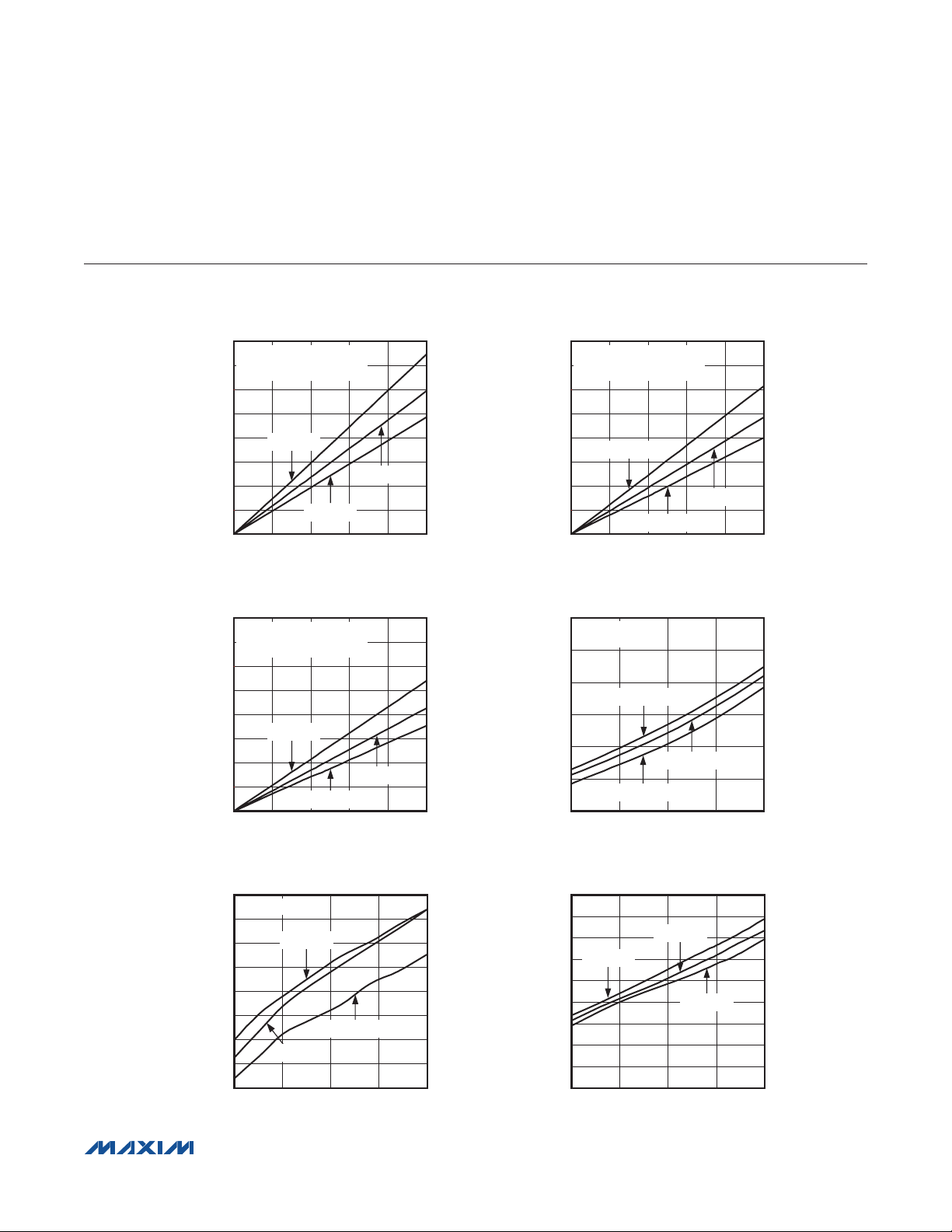
Typical Operating Characteristics
C-Interfaced 8 x 7
GPO OUTPUT LOW VOLTAGE
vs. SINK CURRENT (GPIO4–GPIO0)
40
VDD = 2.4V
35
LOW-SIDE OPEN-DRAIN MODE
30
25
20
15
10
GPO OUTPUT LOW VOLTAGE (mV)
5
0
TA = +85°C
TA = +25°C
TA = -40°C
0 5
SINK CURRENT (mA)
GPO OUTPUT LOW VOLTAGE
vs. SINK CURRENT (GPIO4–GPIO0)
40
VDD = 3.6V
35
LOW-SIDE OPEN-DRAIN MODE
30
25
20
15
10
GPO OUTPUT LOW VOLTAGE (mV)
5
0
TA = +85°C
TA = +25°C
TA = -40°C
0 5
SINK CURRENT (mA)
KEY-SWITCH SOURCE CURRENT
vs. SUPPLY VOLTAGE
28.0
COL0 = V
27.8
27.6
27.4
27.2
27.0
26.8
KEY-SWITCH SOURCE CURRENT (µA)
26.6
26.4
1.6 3.6
GND
TA = +25°C
TA = -40°C
TA = +85°C
SUPPLY VOLTAGE (V)
GPO OUTPUT LOW VOLTAGE
vs. SINK CURRENT (GPIO4–GPIO0)
40
VDD = 3.0V
35
MAX7365 toc01
431 2
LOW-SIDE OPEN-DRAIN MODE
30
25
20
15
10
GPO OUTPUT LOW VOLTAGE (mV)
5
0
TA = +85°C
TA = -40°C
0 5
SINK CURRENT (mA)
MAX7365 toc02
TA = +25°C
431 2
SUPPLY CURRENT vs. SUPPLY VOLTAGE
60
AUTOSLEEP = OFF
GPI = STANDBY MODE
MAX7365 toc03
431 2
55
50
45
40
SUPPLY CURRENT (µA)
35
30
1.6 3.6
TA = +85°C
TA = +25°C
TA = -40°C
SUPPLY VOLTAGE (V)
3.12.62.1
MAX7365 toc04
SLEEP MODE SUPPLY CURRENT
vs. SUPPLY VOLTAGE
1.8
MAX7365 toc05
3.12.62.1
1.6
1.4
TA = +85°C
1.2
1.0
0.8
0.6
0.4
SLEEP MODE SUPPLY CURRENT (µA)
0.2
0
1.6 3.6
TA = +25°C
TA = -40°C
SUPPLY VOLTAGE (V)
3.12.62.1
MAX7365 toc06
����������������������������������������������������������������� Maxim Integrated Products 4
MAX7365
2
1MHz I
C-Interfaced 8 x 7
Key-Switch Controller with GPIO Ports
Pin Configuration
TOP VIEW
(BUMP SIDE DOWN)
MAX7365
1 2 3 4
+
A
ROW6
B
ROW4
C
ROW2
D
ROW1
E
ROW0
BUMP NAME FUNCTION
A1 ROW6 Row 6 Input from Key Matrix or General-Purpose Input
A2 ROW7 Row 7 Input from Key Matrix or General-Purpose Input
A3 COL2 Column 2 Input from Key Matrix or General-Purpose Input
A4 COL3 Column 3 Input from Key Matrix or General-Purpose Input
A5 COL4 Column 4 Input from Key Matrix or General-Purpose Input
B1 ROW4 Row 4 Input from Key Matrix or General-Purpose Input
B2 ROW5 Row 5 Input from Key Matrix or General-Purpose Input
B3 COL1 Column 1 Input from Key Matrix or General-Purpose Input
B4 COL6 Column 6 Input from Key Matrix or General-Purpose Input
B5 COL5 Column 5 Input from Key Matrix or General-Purpose Input
C1 ROW2 Row 2 Input from Key Matrix or General-Purpose Input
C2 ROW3 Row 3 Input from Key Matrix or General-Purpose Input
C3 COL0 Column 0 Input from Key Matrix or General-Purpose Input
C4 GPIO0 General-Purpose Input/Output Port 0
ROW7 COL2 COL3 COL4
ROW5 COL1 COL6 COL5
ROW3 COL0 GPIO0 GND
V
DD
INT SCL GPIO3 GPIO2
SDA GPIO4 GPIO1
WLP
5
Pin Description
����������������������������������������������������������������� Maxim Integrated Products 5
2
1MHz I
C-Interfaced 8 x 7
Key-Switch Controller with GPIO Ports
Pin Description (continued)
BUMP NAME FUNCTION
C5 GND Ground
D1 ROW1 Row 1 Input from Key Matrix or General-Purpose Input
D2 V
DD
D3 SDA I
D4 GPIO4 General-Purpose Input/Output Port 4
D5 GPIO1 General-Purpose Input/Output Port 1
E1 ROW0 Row 0 Input from Key Matrix or General-Purpose Input
E2
INT Active-Low Key-Switch Interrupt Output. INT is open drain and requires a pullup resistor.
E3 SCL I
E4 GPIO3 General-Purpose Input/Output Port 3
E5 GPIO2 General-Purpose Input/Output Port 2
Positive Supply Voltage. Bypass to GND with a 0.1FF capacitor as close as possible to the device.
2
C-Compatible Serial-Data Input/Output
2
C-Compatible Serial-Clock Input
MAX7365
INT
SDA
SCL
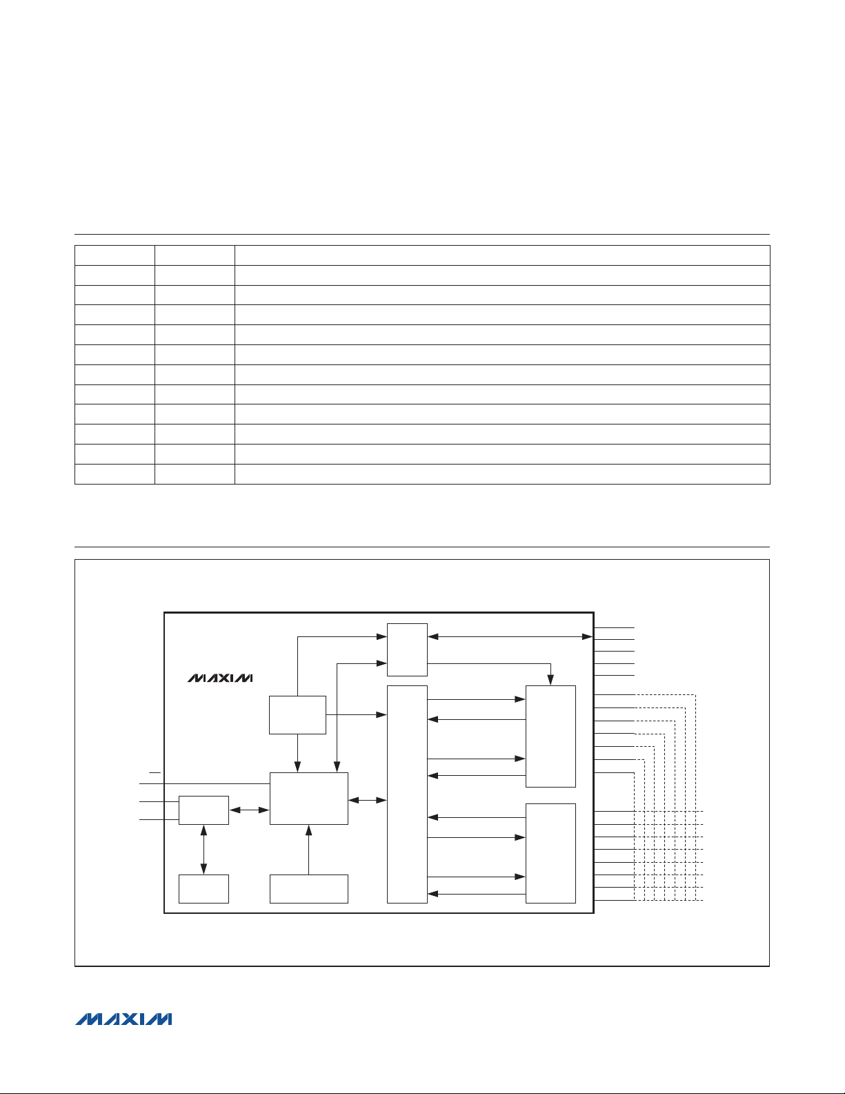
MAX7365
I2C
INTERFACE
BUS
TIMEOUT
OSCILLATOR
CONTROL
REGISTERS FIFO
POR
GPIO
LOGIC
KEY-
SCAN
LOGIC
COLUMN ENABLE
CURRENT DETECT
GPI ENABLE
GPI INPUT
ROW ENABLE
ROW DETECT
GPI ENABLE
GPI INPUT
CURRENT
SOURCE
COLUMN
DRIVES/
GPI
ROW
DRIVES/
GPI
Functional Diagram
GPIO0
GPIO1
GPIO2
GPIO3
GPIO4
COL0
COL1
COL2
COL3
COL4
COL5
COL6
ROW0
ROW1
ROW2
ROW3
ROW4
ROW5
ROW6
ROW7
����������������������������������������������������������������� Maxim Integrated Products 6
MAX7365
2
1MHz I
C-Interfaced 8 x 7
Key-Switch Controller with GPIO Ports
Detailed Description
the device cannot enter autosleep. The autowake feature
takes the device out of sleep mode following a keypress
The MAX7365 is a microprocessor peripheral low-noise,
key-switch controller that monitors up to 56 key switches
with optional autorepeat. Key events are presented in a
16-byte FIFO. Key-switch functionality can be traded to
provide up to 16 logic inputs. The device features an additional five GPIOs. Outputs configured as open drain feature an optional on-chip 100kI pullup/pulldown resistor.
The device features an automatic sleep mode and automatic wakeup that further reduce supply current con-
event. Autosleep and autowake can be disabled.
Interrupt requests can be configured to be issued on a
programmable number of FIFO entries or can be set to
a period of time to prevent overloading the microproces-
sor with too many interrupts. The key-switch status can
be checked at any time by reading the key-switch FIFO.
A 1-byte read access returns both the next key-event in
the FIFO, if there is one, and the FIFO status. Interrupts
are configurable per each input port with edge detection.
sumption. The device can be configured to enter sleep
mode after a programmable time following a key event.
The FIFO content is maintained during sleep mode and
can be read in sleep mode. When a key is held down,
On power-up, all control registers are set to power-up
values (Table 1), and the device is in sleep mode.
Table 1. Register Address Map and Power-Up Condition
ADDRESS
CODE (hex)
0x00 Read only 0x3F Keys FIFO Read FIFO keyscan data out
0x01
0x02
0x03
0x05
0x06
0x30
0x31
0x32
0x33 Read only 0xFF GPIs LSB Value GPI[7:0] (ROW0, COL[6:0]) port input values
0x34 Read only 0x7F GPIs MSB Value GPI[14:8] (ROW[7:1]) port input values
0x35
0x36
0x37
0x38
0x39
0x3A
0x3B
0x3C
READ/
WRITE
R/W
R/W
R/W
R/W
R/W
R/W
R/W
R/W
R/W
R/W
R/W
R/W
R/W
R/W
R/W
R/W
POWER-UP
VALUE (hex)
0x0B Configuration
0xFF Key-Switch Debounce Key debounce time setting
0x00 Key-Switch Interrupt
0x00 Key-Switch Autorepeat Delay and frequency for key repeat
0x07 Autosleep Idle time to autosleep
0xF7 Key-Switch Array Size Keyscan switch array size
0x00 GPIO Direction Select GPIO port as input mode or output mode
0x00 GPO Output Mode GPO open-drain/push-pull output setting for GPIO port
0x1F GPIO Value Debounced input or output values for GPIO port
0x1F GPIs Interrupt Mask GPIO port interrupt mask for inputs
0xFF GPIs LSB Interrupt Mask GPI[7:0] (ROW0, COL[6:0]) port interrupt mask for inputs
0x7F GPIs MSB Interrupt Mask GPI[14:8] (ROW[7:1]) port interrupt mask for inputs
0x00 GPIs Interrupt Trigger GPIO edge-triggered interrupt setting
0x00
0x00
0x00
REGISTER
FUNCTION
GPIs LSB Interrupt
Trigger Mode
GPIs MSB Interrupt
Trigger Mode
GPO High-Side
Open-Drain Enable
DESCRIPTION
Power-down, interrupt clearing mode, key-release enable,
autowake, and I
Key-switch interrupt and INT frequency setting
GPI[7:0] (ROW0, COL[6:0]) edge-triggered interrupt setting
GPI[14:8] (ROW[7:1]) edge-triggered interrupt setting
GPIO port output mode high-side open-drain setting
2
C timeout enable
Register Description
����������������������������������������������������������������� Maxim Integrated Products 7
2
1MHz I
C-Interfaced 8 x 7
Key-Switch Controller with GPIO Ports
Table 1. Register Address Map and Power-Up Condition (continued)
MAX7365
ADDRESS
CODE (hex)
0x3D
0x40
0x42
0x48
READ/
WRITE
R/W
R/W
R/W
R/W
POWER-UP
VALUE (hex)
0x00
0x00
0x00 GPI Debounce Setting GPIO port inputs debounce time setting
0x00 I
REGISTER FUNCTION DESCRIPTION
GPO Pullup/Pulldown
Resistor Enable
GPIO Global
Configuration
2
C Timeout Flag I2C timeout since last POR
GPIO port open-drain output mode pullup/pulldown resistor
setting
2
GPI autowake enable, I
mode
C timeout interrupt enable, operating
Table 2. Key-Switch Mapping
PIN COL0 COL1 COL2 COL3 COL4 COL5 COL6
ROW0
ROW1
ROW2
ROW3
ROW4
ROW5
ROW6
ROW7
KEY 0 KEY 8 KEY 16 KEY 24 KEY 32 KEY 40 KEY 48
KEY 1 KEY 9 KEY 17 KEY 25 KEY 33 KEY 41 KEY 49
KEY 2 KEY 10 KEY 18 KEY 26 KEY 34 KEY 42 KEY 50
KEY 3 KEY 11 KEY 19 KEY 27 KEY 35 KEY 43 KEY 51
KEY 4 KEY 12 KEY 20 KEY 28 KEY 36 KEY 44 KEY 52
KEY 5 KEY 13 KEY 21 KEY 29 KEY 37 KEY 45 KEY 53
KEY 6 KEY 14 KEY 22 KEY 30 KEY 38 KEY 46 KEY 54
KEY 7 KEY 15 KEY 23 KEY 31 KEY 39 KEY 47 KEY 55
Keyscan Controller
Key inputs are scanned statically, not dynamically, to
ensure low-EMI operation. Since inputs only toggle in
response to switch changes, the key matrix can be
routed closer to sensitive circuit nodes.
The keyscan controller debounces and maintains a FIFO
buffer of keypress and release events (including autorepeated keypresses, if autorepeat is enabled). Table 2
shows the key-switch order. The user-programmable
key-switch debounce time and autosleep timer are
derived from the clock, which in turn is derived from the
internal oscillator. Time delay for autorepeat and keyswitch interrupt is based on the key-switch debounce
time. There is no limitation for the number of keys pressed
simultaneously as long as no ghost keys are generated.
If the application requires fewer keys to be scanned, the
unused key-switch ports can be configured as GPIs.
����������������������������������������������������������������� Maxim Integrated Products 8
Keys FIFO Register (0x00)
The Keys FIFO register contains the information pertain-
ing to the status of the keys FIFO, as well as the key
events that have been debounced (Table 6). Bits D[5:0]
denote which of the 56 keys have been debounced, and
the keys are numbered as shown in Table 2.
Special codes are key repeat (0x1E/0x3E), FIFO empty
(0x3F), and FIFO overflow (0x7F). Bit D7 indicates if there
is more data in the FIFO, except when a special key code
occurs. D6 indicates if a keypress or release event has
occurred.
Reading the keyscan FIFO clears the interrupt (INT),
depending on the setting of bit D5 in the configuration
register (0x01).

MAX7365
2
1MHz I
C-Interfaced 8 x 7
Key-Switch Controller with GPIO Ports
Configuration Register (0x01)
The Configuration register controls the I
out feature, enables the key-release indicator, enables
autowake, and determines how INT is deasserted. Write
to bit D7 to put the device into sleep or operating mode.
Autosleep and autowake, when enabled, also change the
status of D7 (Table 7).
Key-Switch Debounce Register (0x02)
The Key-Switch Debounce register sets the keypress and
key-release time for each debounce cycle. Bits D[3:0]
set the debounce time for keypresses, while bits D[7:4]
set the debounce time for key releases. Both debounce
times are configured in increments of 2ms starting at 1ms
and ending at 31ms (Table 8).
Key-Switch Interrupt Register (0x03)
The Key-Switch Interrupt register contains information
related to the settings of the interrupt request function,
as well as the status of the INT output. If bits D[7:0]
are set to 0x00, INT is disabled. There are two types of
interrupts, the FIFO-based interrupt and the time-based
interrupt. Set bits D[4:0] to assert interrupts at the end
of the selected number of debounce cycles following
a key event (Table 9). This number ranges from 1–31
debounce cycles. Setting bits D[7:5] sets the FIFObased interrupt when there are 2–14 key events stored
in the FIFO. Both interrupts can be configured simultaneously, and INT asserts depending on which condition is
met first. INT deasserts depending on the status of bit D5
in the Configuration register.
Key-Switch Autorepeat Register (0x05)
The device’s autorepeat feature notifies the host that at
least one key has been pressed for a continuous period.
The Autorepeat register enables or disables this feature,
sets the time delay after the last key event before the key
repeat code (0x7E) is entered into the FIFO, and sets
the frequency at which the key-repeat code is entered
into the FIFO thereafter. The autorepeat code continues
to be entered in the FIFO at the frequency set by bits
D[3:0] until another key event is recorded. The key being
pressed is not entered again into the FIFO. Following
the key-release event, if any keys are still pressed, the
device restarts the autorepeat sequence. Bit D7 specifies whether the autorepeat function is enabled with 0
denoting autorepeat disabled, and 1 denoting autorepeat enabled. Bits D[3:0] specify the autorepeat delay in
2
C bus time-
terms of debounce cycles, ranging from 8–128 debounce
cycles (Table 10). Bits D[6:4] specify the autorepeat rate
or frequency ranging from 4–32 debounce cycles.
Autosleep Register (0x06)
Autosleep puts the device in sleep mode to draw
minimal current. When enabled, the device enters sleep
mode if no keys are pressed for the autoshutdown time
(Table 11).
Key-Switch Array Size Register (0x30)
Bits D[7:4] set the row size of the key-switch array, and
bits D[3:0] set the column size of the key-switch array
(see Table 12). Set the bits to 0 if no key switches are
used. The key-switch array should be connected begin-
ning at ROW0 and COL0. If not used as a key-switch-
matrix pin, the pin can function as a GPI port, if enabled.
Key-Switch Autosleep Mode
In sleep mode, the device draws minimal current. Switch-
matrix current sources are turned off and become high.
When autosleep is enabled, key-switch inactivity for a
period longer than the autosleep time puts the part into
sleep mode (FIFO data is maintained). Writing a 1 to
D7 in the Configuration register (0x01) or a keypress
can take the device out of sleep mode. Bit D7 in the
Configuration register gives the sleep-mode status and
can be read at any time.
To place the device in sleep mode, clear bit D7 in the
Configuration register. The device is in sleep mode
after power-on reset (POR). In sleep mode, the keyscan
controller is disabled and the device draws minimal cur-
rent. No additional supply current is drawn if no keys are
pressed. All switch-matrix current sources are turned
off, and the row outputs (ROW7–ROW0) are low and the
column outputs (COL6–COL0) become high.
To take the device out of sleep mode and into operating
mode, cause a low-to-high transition in bit D7 by setting it
to a 1 in the Configuration register. The keyscan control-
ler FIFO buffers are cleared and key monitoring starts.
Note that rewriting the Configuration register bit D7 to a
1, when bit D7 is already a 1, does not clear the FIFOs.
The FIFOs are only cleared when the device is changing
state from shutdown to operating mode.
In sleep mode, the internal oscillator is disabled and the
2
C timeout features are disabled.
I
����������������������������������������������������������������� Maxim Integrated Products 9
MAX7365
2
1MHz I
C-Interfaced 8 x 7
Key-Switch Controller with GPIO Ports
Key-Switch Autowake
Keypresses initiate autowake and the device goes into
operating mode. Keypresses that autowake the device
are not lost. When a key is pressed while the device is in
sleep mode, all analog circuitry, including switch-matrix
current sources, turn on in 2ms. The initial key needs to
be pressed for 2ms plus the debounce time to be stored
in the FIFO. Write a 0 to bit D1 in the Configuration register (0x01) to disable autowake.
FIFO Overflow
The FIFO overflow status occurs when the FIFO is full
(16 bytes) and additional events occur. If key release is
disabled, then the FIFO overflow status occurs when the
FIFO is full and not upon additional key events. When the
FIFO is overflowed, the first byte read from the FIFO buffer is the overflow byte (0x7F). The order of the original 16
bytes of event data is preserved, but further events could
be lost. When the FIFO is full, if the 18th key event is a key
release, then the FIFO overflow status is removed.
GPIO Ports
The device has five GPIO ports. The ports can be used
as logic inputs or logic outputs. Each GPIO port features
pullup/pulldown resistors when configured as open-drain
outputs. Also, the port is configurable with a high-side
open-drain output.
The COLs (GPI[6:0]) and ROWs (GPI[14:7]) are also
configurable as GPIs when not used for the key-switch
matrix. When the device is configured with C columns
and R rows for the key-switch matrix, assuming N is the
larger number between R and C, then COL[6:N+1] and
ROW[7:N+1] are configured as GPI ports. As an example, for a 4 x 4 matrix, COL6/COL5 and ROW7, ROW6,
and ROW5 are configured as GPIs, as shown in Table 3.
Unused GPIs and pins configured neither as key-switch
nor GPI should be connected to GND. Table 4, config-
ured as a 3 x 4 matrix, shows ROW4 and ROW3 con-
nected to GND, since they cannot be configured as GPI.
GPIO Direction Register (0x31)
This register configures the pins as an input or an output
port. GPIO Direction register bits D[4:0] correspond with
GPIO4–GPIO0 (Table 13). Set the corresponding bit to
0 to configure it as an input and 1 to configure it as an
output.
When the port is initially programmed as an input, there
is a delay of one debounce period prior to detecting
a transition on the input port. This is to prevent a false
interrupt from occurring when changing a port from an
output to an input.
GPO Output Mode Register (0x32)
This register configures the pin as an open-drain or
push-pull output. GPO Output Mode register bits D[4:0]
correspond with GPIO4–GPIO0 (Table 14). Set the cor-
responding bit to 0 to configure the output mode as open
drain and 1 to configure the output mode as push-pull.
GPIs LSB, MSB Port Value Registers
(0x33, 0x34) (Read Only)
The GPIs LSB and MSB Port Value registers contain the
debounced input data for all the GPIOs for GPI[7:0] and
GPI[14:8], respectively (Table 15 and Table 16). There is
one debounce period delay prior to detecting a transi-
tion on the input port. This prevents a false interrupt from
occurring when changing a port from an output to an
input. These registers report the state of all input ports,
regardless of any interrupt mask settings.
Table 3. 4 x 4 Keyboard Matrix
Configuration with GPI
ROWS
0
1
2
3
4
5
6
7
0 1 2 3 4 5 6
4 x 4 keyboard
matrix
GND — — —
GPI — — —
GPI — — —
GPI — — —
���������������������������������������������������������������� Maxim Integrated Products 10
COLUMNS
GND GPI GPI
Table 4. 3 x 4 Keyboard Matrix
Configuration with GPI
ROWS
0
1
2
3
4
5
6
7
0 1 2 3 4 5 6
3 x 4 keyboard
matrix
GND — — —
GND — — —
GPI — — —
GPI — — —
GPI — — —
COLUMNS
GND GPI GPI

MAX7365
2
1MHz I
C-Interfaced 8 x 7
Key-Switch Controller with GPIO Ports
GPIO Value Register (0x35)
The GPIO Value register consists of a read and write mode
for the GPIO4–GPIO0 pins (Table 17). When read, this reg-
ister reports the debounced input values for ports configured as a GPI. There is one debounce period delay prior
to detecting a transition on the input port. This prevents a
false interrupt from occurring when changing a port from
an output to an input. This register reports the state of all
input ports, regardless of any interrupt mask settings.
When written, this register sets the output as logic-low
when written logic 0, or as logic-high when written logic
1 for ports configured as GPO.
GPIs, LSB, MSB Interrupt Mask Registers
(0x36, 0x37, 0x38)
The GPIs, LSB, and MSB Interrupt Mask registers
control which ports trigger an interrupt (Table 18 for
GPIO4–GPIO0, Table 19 for GPI[7:0], and Table 20 for
GPI[14:8]). Set the bit to logic 0 to enable the interrupt.
Set the bit to logic 1 to mask the interrupt.
If the port that generated the interrupt is not masked, then
the interrupt causes the INT signal to assert. A read of the
port value registers (0x33 to 0x35) is required to deassert
the INT pin. Note that transitions that occur while INT is
asserted, but before the read of the port value registers,
set the appropriate bit of the port value registers only, but
have no affect on the INT pin as it is already asserted.
2
However, transitions that occur when the I
cannot be latched into the port values registers until
after the read has taken place. If there are transitions
that cause the INT signal to assert during the time of an
2
C read, they cause the INT signal to reassert once the
I
read transaction has taken place. Note that the interrupt
configurations only apply when a port is configured as
an input.
GPIs, LSB, MSB Interrupt Trigger Registers
(0x39, 0x3A, 0x3B)
The GPIs, LSB, and MSB Interrupt Trigger registers
control how an interrupt is triggered (Table 21 for
GPIO4–GPIO0, Table 22 for GPI[7:0], and Table 23 for
GPI[14:8]). Set the bit to logic 0 for rising edge-triggered
interrupts. Set the bit to logic 1 for both rising and falling
edge-trigged interrupts.
C is active
GPO High-Side Open-Drain Enable Register (0x3C)
This register allows for high-side open-drain mode for
GPIO4–GPIO0 (see Table 24). Set the bit to logic 0 for
low-side open-drain mode. Set the bit to logic 1 to enable
high-side open-drain mode.
GPO Pullup/Pulldown Resister Enable Register
(0x3D)
This register enables the GPO 100kI pullup resistor in
low-side open-drain mode or pulldown resistor in high-
side open-drain mode for GPIO4–GPIO0 (Table 25). Set
the bit to logic 0 to disable the internal pullup. Set the bit
to logic 1 to enable the internal pullup.
GPIO Global Configuration Register (0x40)
The GPIO Global Configuration register controls the main
settings for the GPIO ports (Table 26). Bit D5 enables
interrupt generation for I
bit for the GPIs. Set bit D4 to logic 1 for normal GPIO oper-
ation for GPIO_, and ROW_ and COL_ configured as GPIs.
GPIO_ configured as GPOs are automatically enabled.
GPI Debounce Setting Register (0x42)
The GPI Debounce Setting register sets the amount of
time an input must be held in order for the device to reg-
ister a logic transition (Table 27). The GPIO debounce
setting is independent of the key-switch debounce set-
ting. Bits D[4:0] set the 32 possible debounce times from
9ms up to 40ms.
2
C Timeout Flag Register (0x48) (Read Only)
I
2
C Timeout Flag register contains a single bit (D0)
The I
that indicates if an I
28). Read this register to clear an I
interrupt.
2
C timeouts. Bit D4 is the enable
2
C timeout has occurred (Table
2
C timeout-initiated
Interrupts
Three possible sources generate INT: key-switch FIFO
level/debounce cycle settings, I
configured as inputs (registers 0x01 or 0x40, 0x39 –
0x3A). Read the respective data/status registers for each
type of interrupt to clear INT. If multiple sources generate
the interrupt, all the related status registers must be read
to clear INT.
2
C timeout, and GPIOs
���������������������������������������������������������������� Maxim Integrated Products 11

MAX7365
2
1MHz I
C-Interfaced 8 x 7
Key-Switch Controller with GPIO Ports
Serial Interface
The device operates as a slave that sends and receives
data through an I
interface uses a serial-data line (SDA) and a serialclock line (SCL) to achieve bidirectional communication
between master(s) and slave(s). A master (typically a
microcontroller) initiates all data transfers to and from the
device and generates the SCL clock that synchronizes
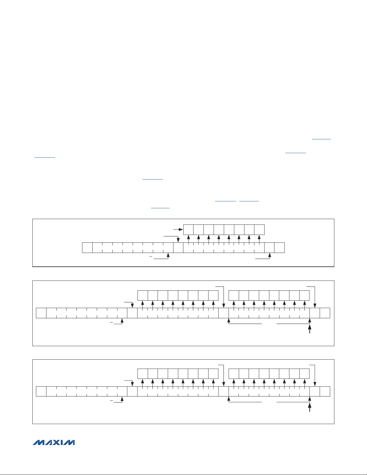
the data transfer. Figure 1 shows the two-wire serial inter-
face timing details.
The device’s SDA line operates as both an input and an
open-drain output. A pullup resistor, typically 4.7kI, is
required on SDA. The device’s SCL line operates only
as an input. A pullup resistor is required on SCL if there
SDA
2
C-compatible two-wire interface. The
t
SU, DAT
t
LOW
t
HD, DAT
t
are multiple masters on the two-wire interface, or if the
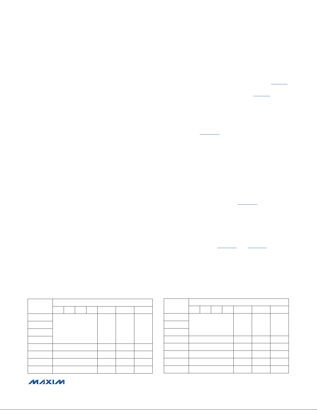
master in a single-master system has an open-drain SCL
output.
Each transmission consists of a START (S) condition
(Figure 2) sent by a master, followed by the device’s 7-bit
slave address plus R/W bit, a register address byte, one
or more data bytes, and finally, a STOP (P) condition.
START and STOP Condition
Both SCL and SDA remain high when the interface is not
busy. A master signals the beginning of a transmission
with a START condition by transitioning SDA from high
to low while SCL is high. When the master has finished
communicating with the slave, it issues a STOP condition
by transitioning SDA from low to high while SCL is high.
The bus is then free for another transmission.
t
SU, STA
R
t
HD, STA
t
SU, STO
t
t
F
F, TX
t
BUF
t
SCL
t
HD, STA
START
CONDITION
HIGH
t
t
R
F
Figure 1. Two-Wire Serial Interface Timing Details
SDA
SCL
S
START
CONDITION
Figure 2. START and STOP Conditions
���������������������������������������������������������������� Maxim Integrated Products 12
REPEATED
START CONDITION
STOP
CONDITION
CONDITION
START
CONDITION
P
STOP

MAX7365
2
1MHz I
C-Interfaced 8 x 7
Key-Switch Controller with GPIO Ports
Bit Transfer
One data bit is transferred during each clock pulse
(Figure 3). The data on SDA must remain stable while
SCL is high.
Acknowledge
The acknowledge bit is a clocked 9th bit (Figure 4), which
the recipient uses to handshake receipt of each byte of
data. Thus, each byte transferred effectively requires 9
bits. The master generates the 9th clock pulse, and the
recipient pulls down SDA during the acknowledge clock
pulse; therefore, the SDA line is stable low during the
high period of the clock pulse. When the master is transmitting to the device, the device generates the acknowledge bit because the device is the recipient. When the
device is transmitting to the master, the master generates
the acknowledge bit because the master is the recipient.
Slave Addresses
The device has a 7-bit long slave address of 0x70, 0x72,
0x74, or 0x76 as determined by the suffix of the complete
part number. The bit following a 7-bit slave address is the
SDA
R/W bit, which is low for a write command and high for a
read command.
The device monitors the bus continuously waiting for a
START condition, followed by its slave address. When
the device recognizes its slave address, it acknowledges
and is then ready for continued communication.
Bus Timeout
The device features a 20ms (min) bus timeout on the two-
wire serial interface, largely to prevent the device from
holding the SDA I/O low during a read transaction should
the SCL lock up for any reason before a serial transac-
tion is completed. Bus timeout operates by causing the
device to internally terminate a serial transaction (either
read or write) if the time between adjacent edges on SCL
exceeds 20ms. After a bus timeout, the device waits for
a valid START condition before responding to a consecu-
tive transmission. This feature can be enabled or dis-
abled under user control by writing to the Configuration
register. In sleep mode, the internal oscillator is disabled,
thus the bus timeout feature is not active.
SCL
Figure 3. Bit Transfer
TRANSMITTER
Figure 4. Acknowledge
���������������������������������������������������������������� Maxim Integrated Products 13
SCL
SDA BY
SDA BY
RECEIVER
DATA LINE STABLE;
START
CONDITION
S
DATA VALID
CHANGE OF DATA
ALLOWED
CLOCK PULSE FOR
ACKNOWLEDGE
1 2 8 9
MAX7365
2
1MHz I
C-Interfaced 8 x 7
Key-Switch Controller with GPIO Ports
Message Format for Writing
the Keyscan Controller
A write to the device comprises the transmission of the
slave address with the R/W bit set to zero, followed by at
least 1 byte of information. The first byte of information is
the command byte. The command byte determines which
register of the device is to be written by the next byte, if
received. If a STOP condition is detected after the command byte is received, the device takes no further action
(Figure 5) beyond storing the command byte.
Any bytes received after the command byte are data
bytes. The first data byte goes into the internal register of
the device selected by the command byte (Figure 6).
If multiple data bytes are transmitted before a STOP condition is detected, these bytes are generally stored insubsequent internal registers of the device because the command-byte address generally autoincrements
COMMAND BYTE IS STORED ON RECEIPT OF
ACKNOWLEDGE FROM MAX7365
S A A P0SLAVE ADDRESS COMMAND BYTE
(Table 5).
ACKNOWLEDGE CONDITION
R/W
Message Format for Reading
the Keyscan Controller
The device is read using the internally stored command
byte as an address pointer, the same way the stored
command byte is used as an address pointer for a write.
The pointer generally autoincrements after each data
byte is read using the same rules as for a write (Table 5).
Thus, a read is initiated by first configuring the device’s
command byte by performing a write (Figure 5). The mas-
ter can now read N consecutive bytes from the device,
with the first data byte being read from the register
addressed by the initialized command byte. When per-
forming read-after-write verification, remember to reset
the command byte’s address because the stored com-
mand byte address is generally autoincremented after
the write (Figure 7, Table 5).
D7 D6 D5 D4 D3 D2 D1 D0
ACKNOWLEDGE FROM MAX7365
Figure 5. Command Byte Received
ACKNOWLEDGE FROM MAX7365
D7 D6 D5 D4 D3 D2 D1 D0 D1 D0D3 D2D5 D4D7 D6
ACKNOWLEDGE FROM MAX7365
S A A A P0SLAVE ADDRESS COMMAND BYTE DATA BYTE
R/W
Figure 6. Command and Single Data Byte Received
ACKNOWLEDGE FROM MAX7365
D7 D6 D5 D4 D3 D2 D1 D0 D1 D0D3 D2D5 D4D7 D6
ACKNOWLEDGE FROM MAX7365
S A A A P0SLAVE ADDRESS COMMAND BYTE DATA BYTE
R/W
Figure 7. N Data Bytes Received
���������������������������������������������������������������� Maxim Integrated Products 14
ACKNOWLEDGE FROM MAX7365
ACKNOWLEDGE FROM MAX7365
1 BYTE
AUTOINCREMENT
COMMAND BYTE ADDRESS
N BYTES
AUTOINCREMENT
COMMAND BYTE ADDRESS

MAX7365
2
1MHz I
C-Interfaced 8 x 7
Key-Switch Controller with GPIO Ports
Operation with Multiple Masters
When the device is operated on a two-wire interface with
multiple masters, a master reading the device uses a
repeated START between the write that sets the device’s
address pointer and the read(s) that takes the data from
the location(s). This is because it is possible for master
2 to take over the bus after master 1 has set up the
device’s address pointer, but before master 1 has read
the data. If master 2 subsequently resets the device’s
address pointer, master 1’s read can be from an unexpected location.
Command Address Autoincrementing
Address autoincrementing allows the device to be
configured with fewer transmissions by minimizing the
number of times the command address needs to be sent.
The command address stored in the device generally
increments after each data byte is written or read (Table
5). Autoincrement only functions when doing a multiburst
read or write.
Applications Information
Reset from I2C
After a catastrophic event such as ESD discharge or
microcontroller reset, use bit D7 of the Configuration register (0x01) as a software reset for the key switches. Use
bit D4 of the GPIO Global Configuration register (0x40)
as a software reset for the GPIOs.
Ghost-Key Elimination
Ghost keys are a phenomenon inherent with key-switch
matrices. When three switches located at the corners
of a matrix rectangle are pressed simultaneously, the
switch that is located at the last corner of the rectangle
(the ghost key) also appears to be pressed. This occurs
because the potentials at the two sides of the ghost-key
switch are identical due to the other three connections—
the switch is electrically shorted by the combination of
the other three switches (Figure 8). Because the key
appears to be pressed electrically, it is impossible to
detect which of the four keys is the ghost key.
The device employs a proprietary scheme that detects
any three-key combination that generates a fourth ghost
key, and does not report the third key that causes a
ghost-key event. This means that although ghost keys
are never reported, many combinations of three keys
are effectively ignored when pressed at the same time.
Applications requiring three-key combinations (such as
<Ctrl><Alt><Del>) must ensure that the three keys are
not wired in positions that define the vertices of a rect-
angle (Figure 9). There is no limit on the number of keys
that can be pressed simultaneously, as long as the keys
do not generate ghost-key events and the FIFO is not full.
REGULAR KEYPRESS
EVENT
GHOST-KEY
EVENT
KEY-SWITCH MATRIX
Figure 8. Ghost-Key Phenomenon
EXAMPLES OF VALID THREE-KEY COMBINATIONS
Table 5. Autoincrement Rules
REGISTER
FUNCTION
Keys FIFO 0x00 0x00
Autosleep 0x06 0x00
All other key 0x01 to 0x05 Addr + 0x01
All other GPIOs 0x30 to 0x48 Addr + 0x01
ADDRESS
CODE (hex)
���������������������������������������������������������������� Maxim Integrated Products 15
AUTOINCREMENT
ADDRESS (hex)
KEY-SWITCH MATRIX KEY-SWITCH MATRIX
Figure 9. Valid Three-Key Combinations

MAX7365
2
1MHz I
C-Interfaced 8 x 7
Key-Switch Controller with GPIO Ports
Low-EMI Operation
The device uses two techniques to minimize EMI radiating from the key-switch wiring. First, the voltage across
the switch matrix never exceeds 0.5V if not in sleep
mode, independent of supply voltage V
the voltage swing at any node when a switch is pressed
to 0.5V (max). Second, the keys are not dynamically
scanned, which would cause the key-switch wiring to
continuously radiate interference. Instead, the keys are
monitored for current draw (only occurs when pressed),
and debounce circuitry only operates when one or more
keys are actually pressed.
. This reduces
DD
Switch On-Resistance
The device is designed to be insensitive to resistance,
either in the key switches, or the switch routing to and
Table 6. Keys FIFO Register (0x00)
SPECIAL FUNCTION
General bit description
FIFO not-empty
from the appropriate COL_ and ROW_ up to 5kI (max).
These controllers are therefore compatible with low-cost
membrane and conductive carbon switches.
Hot Insertion
The INT, SCL, and SDA remain high impedance with up
to 3.6V asserted on them when the device powers down
= 0V). I/O ports remain high impedance with up to
(V
DD
4V asserted on them when not powered. The device can
be used in hot-swap applications.
Power-Supply Considerations
The device operates with a 1.62V to 3.6V power-supply
voltage. Bypass the power supply (V
0.1FF or higher ceramic capacitor as close as possible
to the device.
) to GND with a
DD
Register Tables
KEYS FIFO REGISTER DATA
D7 D6 D5 D4 D3 D2 D1 D0
flag
Key-release
flag
Key number/Key event
Key number indicated by D[5:0] is a keypress. Last
data in the FIFO.
Key number indicated by D[5:0] is a keypress. More
data in the FIFO.
Key number indicated by D[5:0] is a key release. Last
data in the FIFO.
Key number indicated by D[5:0] is a key release. More
data in the FIFO.
FIFO is empty. 0 0 1 1 1 1 1 1
FIFO is overflowed. Continued to read data in the FIFO. 0 1 1 1 1 1 1 1
Key repeat. Indicates the last data in the FIFO. 0 0 1 1 1 1 1 0
Key repeat. Indicates more data in the FIFO. 0 1 1 1 1 1 1 0
���������������������������������������������������������������� Maxim Integrated Products 16
0 0 X X X X X X
1 0 X X X X X X
0 1 X X X X X X
1 1 X X X X X X

Key-Switch Controller with GPIO Ports
Table 7. Configuration Register (0x01)
1MHz I
MAX7365
2
C-Interfaced 8 x 7
REGISTER
BIT
D7 Sleep
D6 Reserved 0 — 0
D5 Interrupt
D4 Reserved 0 — 0
D3
D2 Reserved 0 — 0
D1 Autowake enable
D0 Timeout disable
X = Don’t care.
DESCRIPTION VALUE FUNCTION
Key-switch operating mode. Key switches always remain
active when GPI (bit 4 of register 0x40) is high, regardless of
autosleep, autowake, or an I
Key-switch sleep mode. The
entire chip is shut down.
Key-switch operating mode.
INT cleared when the FIFO is empty.
INT cleared after host read. In this mode, I
FIFO until interrupt condition is removed or further INT could
be lost.
2
C timeout enabled.
2
C timeout disabled.
2
C write to this bit.
2
C write, autosleep, and
I
autowake can all change this
bit. This bit can be read back
2
by I
status.
Key-release
enable
X
(when 0x40 D4 = 1)
0
(when 0x40 D4 = 0)
1
(when 0x40 D4 = 0)
0
1
0 Disable key releases.
1 Enable key releases.
0 Disable keypress wakeup.
1 Enable keypress wakeup.
0 I
1 I
C any time for current
2
C should read the
DEFAULT
VALUE
0
0
1
1
1
���������������������������������������������������������������� Maxim Integrated Products 17

1MHz I
Key-Switch Controller with GPIO Ports
Table 8. Key-Switch Debounce Register (0x02)
MAX7365
2
C-Interfaced 8 x 7
REGISTER DESCRIPTION
DEBOUNCE TIME (ms) RELEASE DEBOUNCE TIME PRESS DEBOUNCE TIME
1
3 0 0 0 1
5 0 0 1 0
7 0 0 1 1
9 0 1 0 0
11 0 1 0 1
D7 D6 D5 D4 D3 D2 D1 D0
X
…
25
27 1 1 0 1
29 1 1 1 0
31 1 1 1 1
1 0 0 0 0
3 0 0 0 1
5 0 0 1 0
7 0 0 1 1
9 0 1 0 0
11 0 1 0 1
…
25 1 1 0 0
27 1 1 0 1
29 1 1 1 0
31 1 1 1 1
Power-on default (31) 1 1 1 1 1 1 1 1
X = Don’t care.
X
…
REGISTER DATA
0 0 0 0
…
1 1 0 0
X
X
���������������������������������������������������������������� Maxim Integrated Products 18

Key-Switch Controller with GPIO Ports
Table 9. Key-Switch Interrupt Register (0x03)
REGISTER DESCRIPTION
Power-up default setting
All INT disabled
Time-based INT disabled
INT asserts every debounce cycle
INT asserts every 2 debounce cycles
…
INT asserts every 29 debounce cycles
INT asserts every 30 debounce cycles
INT asserts every 31 debounce cycles
MAX7365
2
1MHz I
D7 D6 D5 D4 D3 D2 D1 D0
FIFO-BASED INT TIME-BASED INT
0 0 0 0 0 0 0 0
X
X
C-Interfaced 8 x 7
REGISTER DATA
0 0 0 0 0
0 0 0 0 1
0 0 0 1 0
…
1 1 1 0 1
1 1 1 1 0
1 1 1 1 1
FIFO-based INT disabled
INT asserts when the FIFO has 2 key events
INT asserts when the FIFO has 4 key events
…
INT asserts when the FIFO has 10 key events
INT asserts when the FIFO has 12 key events
INT asserts when the FIFO has 14 key events
Both time-based and FIFO-based interrupts active Not all zero Not all zero
X = Don’t care.
0 0 0
0 0 1
0 1 0
…
1 0 1
1 1 0
1 1 1
X
X
���������������������������������������������������������������� Maxim Integrated Products 19

MAX7365
2
1MHz I
C-Interfaced 8 x 7
Key-Switch Controller with GPIO Ports
Table 10. Key-Switch Autorepeat Register (0x05)
REGISTER DATA
REGISTER DESCRIPTION
Autorepeat is disabled 0 X X X X X X X
Autorepeat is enabled 1 Autorepeat rate Autorepeat delay
D7 D6 D5 D4 D3 D2 D1 D0
ENABLE AUTOREPEAT RATE AUTOREPEAT DELAY
Autorepeat delay is 8 debounce cycles 1
Autorepeat delay is 16 debounce cycles 1 0 0 0 1
Autorepeat delay is 24 debounce cycles 1 0 0 1 0
X
…
Autorepeat delay is 112 debounce cycles 1
Autorepeat delay is 120 debounce cycles 1 1 1 1 0
Autorepeat delay is 128 debounce cycles 1 1 1 1 1
Autorepeat frequency is 4 debounce cycles 1 0 0 0
Autorepeat frequency is 12 debounce cycles 1 0 1 0
…
Autorepeat frequency is 24 debounce cycles 1 1 0 1
Autorepeat frequency is 32 debounce cycles 1 1 1 1
Power-on default setting 0 0 0 0 0 0 0 0
X = Don’t care.
X
…
0 0 0 0
…
1 1 0 1
XAutorepeat frequency is 8 debounce cycles 1 0 0 1
XAutorepeat frequency is 28 debounce cycles 1 1 1 0
Table 11. Autosleep Register (0x06)
REGISTER DESCRIPTION
AUTOSLEEP (ms) D7 D6 D5 D4 D3 D2 D1 D0
Disabled 0 0 0 0 0 0 0 0
8192 0 0 0 0 0 0 0 1
4096 0 0 0 0 0 0 1 0
2048 0 0 0 0 0 0 1 1
1024 0 0 0 0 0 1 0 0
512 0 0 0 0 0 1 0 1
256 0 0 0 0 0 1 1 0
256 0 0 0 0 0 1 1 1
Power-up default settings 0 0 0 0 0 1 1 1
RESERVED AUTOSHUTDOWN TIME
REGISTER DATA
���������������������������������������������������������������� Maxim Integrated Products 20

MAX7365
2
1MHz I
C-Interfaced 8 x 7
Key-Switch Controller with GPIO Ports
Table 12. Key-Switch Array Size Register (0x30)
REGISTER DATA
REGISTER DESCRIPTION
No rows are key switches 0 0 0 0
ROW0 is a key switch 0 0 0 1
ROW0 to ROW1 are key switches 0 0 1 0
ROW0 to ROW2 are key switches 0 0 1 1
ROW0 to ROW3 are key switches 0 1 0 0
ROW0 to ROW4 are key switches 0 1 0 1
ROW0 to ROW5 are key switches 0 1 1 0
ROW0 to ROW6 are key switches 0 1 1 1
ROW0 to ROW7 are key switches 1 X X X
No columns are key switches
COL0 is a key switch 0 0 0 1
COL0 to COL1 are key switches 0 0 1 0
COL0 to COL2 are key switches 0 0 1 1
COL0 to COL3 are key switches 0 1 0 0
COL0 to COL4 are key switches 0 1 0 1
COL0 to COL5 are key switches 0 1 1 0
COL0 to COL6 are key switches 0 1 1 1
Power-up default setting 1 1 1 1 0 1 1 1
D7 D6 D5 D4 D3 D2 D1 D0
ROWS COLUMNS
X
0 0 0 0
X
X = Don’t care.
Table 13. GPIO Direction Register (0x31)
REGISTER BIT DESCRIPTION VALUE FUNCTION DEFAULT VALUE
D[7:5] Reserved 000 — 000
D4 GPIO4
D3 GPIO3
D2 GPIO2
D1 GPIO1
D0 GPIO0
���������������������������������������������������������������� Maxim Integrated Products 21
0 Set as input pin
1 Set as output pin
0 Set as input pin
1 Set as output pin
0 Set as input pin
1 Set as output pin
0 Set as input pin
1 Set as output pin
0 Set as input pin
1 Set as output pin
0
0
0
0
0

MAX7365
2
1MHz I
C-Interfaced 8 x 7
Key-Switch Controller with GPIO Ports
Table 14. GPO Output Mode Register (0x32)
REGISTER BIT DESCRIPTION VALUE FUNCTION DEFAULT VALUE
D[7:5] Reserved 000 — 000
D4 GPIO4
D3 GPIO3
D2 GPIO2
D1 GPIO1
D0 GPIO0
Table 15. GPIs LSB Value Register (0x33) (Read Only)
0 Port is an open-drain output
1 Port is a push-pull output
0 Port is an open-drain output
1 Port is a push-pull output
0 Port is an open-drain output
1 Port is a push-pull output
0 Port is an open-drain output
1 Port is a push-pull output
0 Port is an open-drain output
1 Port is a push-pull output
0
0
0
0
0
REGISTER BIT DESCRIPTION VALUE FUNCTION DEFAULT VALUE
D7 ROW0
D6 COL6
D5 COL5
D4 COL4
D3 COL3
D2 COL2
D1 COL1
D0 COL0
0 Input value is low
1 Input value is high
0 Input value is low
1 Input value is high
0 Input value is low
1 Input value is high
0 Input value is low
1 Input value is high
0 Input value is low
1 Input value is high
0 Input value is low
1 Input value is high
0 Input value is low
1 Input value is high
0 Input value is low
1 Input value is high
1
1
1
1
1
1
1
1
���������������������������������������������������������������� Maxim Integrated Products 22

MAX7365
2
1MHz I
C-Interfaced 8 x 7
Key-Switch Controller with GPIO Ports
Table 16. GPIs MSB Value Register (0x34) (Read Only)
REGISTER BIT DESCRIPTION VALUE FUNCTION DEFAULT VALUE
D7 Reserved — — 0
D6 ROW7
D5 ROW6
D4 ROW5
D3 ROW4
D2 ROW3
D1 ROW2
D0 ROW1
0 Input value is low
1 Input value is high
0 Input value is low
1 Input value is high
0 Input value is low
1 Input value is high
0 Input value is low
1 Input value is high
0 Input value is low
1 Input value is high
0 Input value is low
1 Input value is high
0 Input value is low
1 Input value is high
1
1
1
1
1
1
1
Table 17. GPIO Value Register (0x35)
REGISTER BIT DESCRIPTION R/W VALUE FUNCTION DEFAULT VALUE
D[7:5] — — 000 Reserved 000
D4 GPIO4 R
D3 GPIO3 R
D2 GPIO2 R
D1 GPIO1 R
D0 GPIO0 R
D4 GPIO4 W
D3 GPIO3 W
D2 GPIO2 W
D1 GPIO1 W
D0 GPIO0 W
0 Input value is low
1 Input value is high
0 Input value is low
1 Input value is high
0 Input value is low
1 Input value is high
0 Input value is low
1 Input value is high
0 Input value is low
1 Input value is high
0 Set output logic-low
1 Set output logic-high
0 Set output logic-low
1 Set output logic-high
0 Set output logic-low
1 Set output logic-high
0 Set output logic-low
1 Set output logic-high
0 Set output logic-low
1 Set output logic-high
0
0
0
0
0
—
—
—
—
—
���������������������������������������������������������������� Maxim Integrated Products 23

MAX7365
2
1MHz I
C-Interfaced 8 x 7
Key-Switch Controller with GPIO Ports
Table 18. GPIs Interrupt Mask Register (0x36)
REGISTER BIT DESCRIPTION VALUE FUNCTION DEFAULT VALUE
D[7:5] Reserved 000 — 000
D4 GPIO4
D3 GPIO3
D2 GPIO2
D1 GPIO1
D0 GPIO0
0 Interrupt is unmasked
1 Interrupt is masked
0 Interrupt is unmasked
1 Interrupt is masked
0 Interrupt is unmasked
1 Interrupt is masked
0 Interrupt is unmasked
1 Interrupt is masked
0 Interrupt is unmasked
1 Interrupt is masked
1
1
1
1
1
Table 19. GPIs LSB Interrupt Mask Register (0x37)
REGISTER BIT DESCRIPTION VALUE FUNCTION DEFAULT VALUE
D7 ROW0
D6 COL6
D5 COL5
D4 COL4
D3 COL3
D2 COL2
D1 COL1
D0 COL0
0 Interrupt is unmasked
1 Interrupt is masked
0 Interrupt is unmasked
1 Interrupt is masked
0 Interrupt is unmasked
1 Interrupt is masked
0 Interrupt is unmasked
1 Interrupt is masked
0 Interrupt is unmasked
1 Interrupt is masked
0 Interrupt is unmasked
1 Interrupt is masked
0 Interrupt is unmasked
1 Interrupt is masked
0 Interrupt is unmasked
1 Interrupt is masked
1
1
1
1
1
1
1
1
���������������������������������������������������������������� Maxim Integrated Products 24

MAX7365
2
1MHz I
C-Interfaced 8 x 7
Key-Switch Controller with GPIO Ports
Table 20. GPIs MSB Interrupt Mask Register (0x38)
REGISTER BIT DESCRIPTION VALUE FUNCTION DEFAULT VALUE
D7 Reversed — — 0
D6 ROW7
D5 ROW6
D4 ROW5
D3 ROW4
D2 ROW3
D1 ROW2
D0 ROW1
0 Interrupt is unmasked
1 Interrupt is masked
0 Interrupt is unmasked
1 Interrupt is masked
0 Interrupt is unmasked
1 Interrupt is masked
0 Interrupt is unmasked
1 Interrupt is masked
0 Interrupt is unmasked
1 Interrupt is masked
0 Interrupt is unmasked
1 Interrupt is masked
0 Interrupt is unmasked
1 Interrupt is masked
1
1
1
1
1
1
1
Table 21. GPIs Interrupt Trigger Mode Register (0x39)
REGISTER BIT DESCRIPTION VALUE FUNCTION DEFAULT VALUE
D[7:5] Reserved 000 — 000
D4 GPIO4
D3 GPIO3
D2 GPIO2
D1 GPIO1
D0 GPIO0
0 Rising edge-triggered interrupts
1 Rising and falling edge-triggered interrupts
0 Rising edge-triggered interrupts
1 Rising and falling edge-triggered interrupts
0 Rising edge-triggered interrupts
1 Rising and falling edge-triggered interrupts
0 Rising edge-triggered interrupts
1 Rising and falling edge-triggered interrupts
0 Rising edge-triggered interrupts
1 Rising and falling edge-triggered interrupts
0
0
0
0
0
���������������������������������������������������������������� Maxim Integrated Products 25

MAX7365
2
1MHz I
C-Interfaced 8 x 7
Key-Switch Controller with GPIO Ports
Table 22. GPIs LSB Interrupt Trigger Mode Register (0x3A)
REGISTER BIT DESCRIPTION VALUE FUNCTION DEFAULT VALUE
D7 ROW0
D6 COL6
D5 COL5
D4 COL4
D3 COL3
D2 COL2
D1 COL1
D0 COL0
0 Rising edge-triggered interrupts
1 Rising and falling edge-triggered interrupts
0 Rising edge-triggered interrupts
1 Rising and falling edge-triggered interrupts
0 Rising edge-triggered interrupts
1 Rising and falling edge-triggered interrupts
0 Rising edge-triggered interrupts
1 Rising and falling edge-triggered interrupts
0 Rising edge-triggered interrupts
1 Rising and falling edge-triggered interrupts
0 Rising edge-triggered interrupts
1 Rising and falling edge-triggered interrupts
0 Rising edge-triggered interrupts
1 Rising and falling edge-triggered interrupts
0 Rising edge-triggered interrupts
1 Rising and falling edge-triggered interrupts
0
0
0
0
0
0
0
0
Table 23. GPIs MSB Input Interrupt Trigger Mode Register (0x3B)
REGISTER BIT DESCRIPTION VALUE FUNCTION DEFAULT VALUE
D7 — X Don’t care 0
D6 ROW7
D5 ROW6
D4 ROW5
D3 ROW4
D2 ROW3
D1 ROW2
D0 ROW1
���������������������������������������������������������������� Maxim Integrated Products 26
0 Rising edge-triggered interrupts
1 Rising and falling edge-triggered interrupts
0 Rising edge-triggered interrupts
1 Rising and falling edge-triggered interrupts
0 Rising edge-triggered interrupts
1 Rising and falling edge-triggered interrupts
0 Rising edge-triggered interrupts
1 Rising and falling edge-triggered interrupts
0 Rising edge-triggered interrupts
1 Rising and falling edge-triggered interrupts
0 Rising edge-triggered interrupts
1 Rising and falling edge-triggered interrupts
0 Rising edge-triggered interrupts
1 Rising and falling edge-triggered interrupts
0
0
0
0
0
0
0

MAX7365
2
1MHz I
C-Interfaced 8 x 7
Key-Switch Controller with GPIO Ports
Table 24. GPO High-Side Open-Drain Enable Register (0x3C)
REGISTER BIT DESCRIPTION VALUE FUNCTION DEFAULT VALUE
D[7:5] Reserved 000 — 000
D4 GPIO4
D3 GPIO3
D2 GPIO2
D1 GPIO1
D0 GPIO0
0 Set low-side open-drain mode
1 Set high-side open-drain mode
0 Set low-side open-drain mode
1 Set high-side open-drain mode
0 Set low-side open-drain mode
1 Set high-side open-drain mode
0 Set low-side open-drain mode
1 Set high-side open-drain mode
0 Set low-side open-drain mode
1 Set high-side open-drain mode
0
0
0
0
0
Table 25. GPO Pullup/Pulldown Resistor Enable Register (0x3D)
REGISTER BIT DESCRIPTION VALUE FUNCTION DEFAULT VALUE
D[7:5] Reserved 000 — 000
0 Disable internal pullup/pulldown
D4 GPIO4
D3 GPIO3
D2 GPIO2
D1 GPIO1
D0 GPIO0
1
0 Disable internal pullup/pulldown
1
0 Disable internal pullup/pulldown
1
0 Disable internal pullup/pulldown
1
0 Disable internal pullup/pulldown
1
Enable internal pullup/pulldown for opendrain output
Enable internal pullup/pulldown for opendrain output
Enable internal pullup/pulldown for opendrain output
Enable internal pullup/pulldown for opendrain output
Enable internal pullup/pulldown for opendrain output
0
0
0
0
0
���������������������������������������������������������������� Maxim Integrated Products 27

MAX7365
2
1MHz I
C-Interfaced 8 x 7
Key-Switch Controller with GPIO Ports
Table 26. GPIO Global Configuration Register (0x40)
REGISTER BIT DESCRIPTION VALUE FUNCTION DEFAULT VALUE
D[7:6] Reserved 00 — 00
2
0 Disable I
2
I
D5
D4 Operating Mode
D[3:0] Reserved — — 0000
C Interrupt
Timeout Enable
1
0 Standby mode
1 Normal mode
Enable I
serted when a read is performed on the I
timeout flag register (0x48)
Table 27. GPI Debounce Setting Register (0x42)
REGISTER DESCRIPTION
Power-up default setting
Debounce time is 9ms
Debounce time is 10ms 0 0 0 0 0 0 0 1
Debounce time is 11ms 0 0 0 0 0 0 1 0
Debounce time is 12ms 0 0 0 0 0 0 1 1
Debounce time is 37ms 0 0 0 1 1 1 0 0
Debounce time is 38ms 0 0 0 1 1 1 0 1
Debounce time is 39ms 0 0 0 1 1 1 1 0
Debounce time is 40ms 0 0 0 1 1 1 1 1
D7 D6 D5 D4 D3 D2 D1 D0
RESERVED DEBOUNCE TIME
0 0 0 0 0 0 0 0
C timeout interrupt
2
C timeout interrupt. INT is deas-
REGISTER DATA
…
2
C
0
0
Table 28. I2C Timeout Flag Register (0x48) (Read Only)
REGISTER
BIT
D[7:1] Reserved 0000000 — 0000000
D0
DESCRIPTION VALUE FUNCTION
0 No I
I2C Timeout
Flag
���������������������������������������������������������������� Maxim Integrated Products 28
1
2
C timeout has occurred since last read or POR.
2
C timeout has occurred since last read or POR. This bit is
I
reset to zero when a read is performed on this register. I
timeouts must be enabled for this function to work (Table
26).
2
C
DEFAULT
VALUE
0

MAX7365
2
1MHz I
C-Interfaced 8 x 7
Key-Switch Controller with GPIO Ports
Wafer-Level Packaging (WLP) Applications Information
For the latest application details on WLP construction, dimensions, tape-carrier information, PCB techniques, bump-pad
layout, and recommended reflow temperature profile, as well as the latest information on reliability testing results, refer
to Application Note 1891: Wafer-Level Packaging (WLP) and Its Applications, available at www.maxim-ic.com/an1891.
Typical Application Circuit
+1.8V
V
DD
GPIO4I/O
COL6
COL5
COL4
KEY 7
KEY 15
KEY 23
KEY 31
KEY 39 KEY 47 KEY 55
+3.3V
V
CC
µC
GND
SDA
SCL
INT
GPIO3I/O
GPIO2I/O
GPIO1I/O
GPIO0I/O
SDA
SCL
INT
MAX7365
GND
COL3
COL2
COL1
COL0
ROW7
ROW6
ROW5
ROW4
ROW3
ROW2
ROW1
ROW0
KEY 6
KEY 5
KEY 4
KEY 3
KEY 2
KEY 1
KEY 0
KEY 14
KEY 13
KEY 12
KEY 11
KEY 10
KEY 9
KEY 8
KEY 22
KEY 21
KEY 20
KEY 19
KEY 18
KEY 17
KEY 16
KEY 30
KEY 29
KEY 28
KEY 27
KEY 26
KEY 25
KEY 24
KEY 38
KEY 37
KEY 36
KEY 35
KEY 34
KEY 33
KEY 32
KEY 46 KEY 54
KEY 45 KEY 53
KEY 44
KEY 43
KEY 42
KEY 41
KEY 40
KEY 52
KEY 51
KEY 50
KEY 49
KEY 48
���������������������������������������������������������������� Maxim Integrated Products 29

MAX7365
2
1MHz I
C-Interfaced 8 x 7
Key-Switch Controller with GPIO Ports
Ordering Information
PART
MAX7365EWA70+
MAX7365EWA72+
MAX7365EWA74+
MAX7365EWA76+
+Denotes a lead(Pb)-free/RoHS-compliant package.
TEMP
RANGE
-40NC to +85NC
-40NC to +85NC
-40NC to +85NC
-40NC to +85NC
PINPACKAGE
25 WLP 70
25 WLP 72
25 WLP 74
25 WLP 76
2
C
I
ADDRESS
(hex)
Chip Information
PROCESS: BiCMOS
Package Information
For the latest package outline information and land patterns
(footprints), go to www.maxim-ic.com/packages. Note that a
“+”, “#”, or “-” in the package code indicates RoHS status only.
Package drawings may show a different suffix character, but
the drawing pertains to the package regardless of RoHS status.
PACKAGE
TYPE
25 WLP W252B2+1
PACKAGE
CODE
OUTLINE
NO.
21-0180
LAND PATTERN NO.
Refer to
Application Note 1891
���������������������������������������������������������������� Maxim Integrated Products 30

MAX7365
2
1MHz I
C-Interfaced 8 x 7
Key-Switch Controller with GPIO Ports
Revision History
REVISION
NUMBER
0 9/11 Initial release —
REVISION
DATE
DESCRIPTION
PAGES
CHANGED
Maxim cannot assume responsibility for use of any circuitry other than circuitry entirely embodied in a Maxim product. No circuit patent licenses are implied.
Maxim reserves the right to change the circuitry and specifications without notice at any time. The parametric values (min and max limits) shown in the Electrical
Characteristics table are guaranteed. Other parametric values quoted in this data sheet are provided for guidance.
Maxim Integrated Products, 120 San Gabriel Drive, Sunnyvale, CA 94086 408-737-7600 31
©
2011 Maxim Integrated Products Maxim is a registered trademark of Maxim Integrated Products, Inc.
 Loading...