

Page 1
19-3809; Rev 1; 10/05
EVALUATION KIT
AVAILABLE
I2C Port Expander with Eight Inputs and
Maskable Transition Detection
General Description
The MAX7319 2-wire serial-interfaced peripheral features eight input ports with selectable internal pullups,
overvoltage protection to +6V, and transition detection
with interrupt output.
All input ports are continuously monitored for state
changes (transition detection). Transitions are latched,
allowing detection of transient changes. Any combination
of inputs can be selected using the interrupt mask to
assert the INT output. When the MAX7319 is subsequently
accessed through the serial interface, any pending interrupt is cleared.
The +5.5V tolerant RST input clears the serial interface,
terminating any I
MAX7319.
The MAX7319 uses two address inputs with four-level
logic to allow 16 I2C slave addresses. The slave
address also enables or disables internal 40kΩ pullups
in groups of four ports.
The MAX7319 supports hot insertion. All eight input
ports, the serial interface SDA, SCL, AD0, AD2, INT,
and RST remain high impedance in power-down (V+ =
0) with up to +6V asserted on them.
The MAX7319 is one device in a family of pin-compatible
port expanders with a choice of input ports, open-drain
I/O ports, and push-pull output ports (see Table 1).
The MAX7319 is available in 16-pin QSOP and 16-pin
TQFN packages, and is specified over the automotive
temperature range (-40°C to +125°C).
2
C†communication to or from the
Features
♦ 400kHz, +5.5V-Tolerant I2C Serial Interface
♦ +1.71V to +5.5V Operating Voltage
♦ Eight Input Ports with Maskable, Latching
Transition Detection
♦ Input Ports are Overvoltage Protected to +6V
♦ Transient Changes are Latched, Allowing
Detection Between Read Operations
♦ INT Output Alerts Change on Any Selection of
Inputs
♦ AD0 and AD2 Inputs Select from 16 Slave
Addresses
♦ Low 0.6µA (typ) Standby Current
♦ -40°C to +125°C Operating Temperature Range
Ordering Information
PART PIN-PACKAGE TOP MARK PKG CODE
MAX7319AEE+ 16 QSOP — E16-4
MAX7319ATE+ 16 TQFN-EP* ADA T1633-4
Note: All devices specified over -40°C to +125°C operating range.
+Denotes lead-free package.
*EP = Exposed pad.
MAX7319
Cell Phones
SAN/NAS
Servers
Applications
Notebooks
Satellite Radio
Automotive
Pin Configurations, Typical Application Circuit, and
Functional Diagram appear at end of data sheet.
Selector Guide
PART INPUTS INTERRUPT MASK OPEN-DRAIN OUTPUTS PUSH-PULL OUTPUTS
MAX7319 8 Yes — —
MAX7320 — — — 8
MAX7321 Up to 8 — Up to 8 —
MAX7322 4 Yes — 4
MAX7323 Up to 4 — Up to 4 4
MAX7328* — —
MAX7329**
*Second source to PCF8574.
**Second source to PCF8574A.
†
a
P
C
l
S.
________________________________________________________________ Maxim Integrated Products 1
For pricing, delivery, and ordering information, please contact Maxim/Dallas Direct! at
1-888-629-4642, or visit Maxim’s website at www.maxim-ic.com.
Up to 8
—
Up to 8
—
Page 2
MAX7319
I2C Port Expander with Eight Inputs and
Maskable Transition Detection
2 _______________________________________________________________________________________
ABSOLUTE MAXIMUM RATINGS
Stresses beyond those listed under “Absolute Maximum Ratings” may cause permanent damage to the device. These are stress ratings only, and functional
operation of the device at these or any other conditions beyond those indicated in the operational sections of the specifications is not implied. Exposure to
absolute maximum rating conditions for extended periods may affect device reliability.
(All voltages referenced to GND.)
Supply Voltage V+....................................................-0.3V to +6V
SCL, SDA, AD0, AD2, RST, INT, I0–I7......................-0.3V to +6V
SDA Input Current.............................................................. 10mA
INT Input Current ................................................................10mA
Total V+ Current..................................................................50mA
Total GND Current ...........................................................100mA
Continuous Power Dissipation (T
A
= +70°C)
16-Pin QSOP (derate 8.3mW/°C over +70°C)..............667mW
16-Pin TQFN (derate 15.6mW/°C over +70°C) ..........1250mW
Operating Temperature Range .........................-40°C to +125°C
Junction Temperature......................................................+150°C
Storage Temperature Range .............................-65°C to +150°C
Lead Temperature (soldering, 10s) .................................+300°C
ELECTRICAL CHARACTERISTICS
(V+ = +1.71V to +5.5V, TA= -40°C to +125°C, unless otherwise noted. Typical values are at V+ = +3.3V, TA= +25°C.) (Note 1)
PARAMETER SYMBOL CONDITIONS MIN TYP MAX UNITS
Operating Supply Voltage V+
Power-On Reset Voltage V
Standby Current (Interface Idle) I
Supply Current
(Interface Running)
Input High Voltage
SDA, SCL, AD0, AD2, RST, I0–I7
Input Low Voltage
SDA, SCL, AD0, AD2, RST, I0–I7
Input Leakage Current
SDA, SCL, AD0, AD2, RST, I0–I7
Input Capacitance
SDA, SCL, AD0, AD2, RST, I0–I7
Output Low Voltage
SDA
Output Low Voltage
INT
Port Input Pullup Resistor R
POR
STB
I+ f
V
V
I
IH
V
OLSDAISINK
V
OLINTISINK
SCL and SDA and other digital inputs at V+ 0.6 1.5 µA
= 400kHz; other digital inputs at V+ 23 55 µA
SCL
V+ < 1.8V 0.8 x V+
IH
V+ ≥ 1.8V 0.7 x V+
V+ < 1.8V 0.2 x V+
IL
V+ ≥ 1.8V 0.3 x V+
SDA, SCL, AD0, AD2, RST, I0–I7 at V+ or
, I
IL
GND
= 6mA 250 mV
= 5mA 100 250 mV
PU
1.71
-0.2 +0.2 µA
25 40 55 kΩ
5.50 V
1.6 V
10 pF
V
V
Page 3
MAX7319
I2C Port Expander with Eight Inputs and
Maskable Transition Detection
_______________________________________________________________________________________ 3
PORT AND INTERRUPT INT TIMING CHARACTERISTICS
(V+ = +1.71V to +5.5V, TA= -40°C to +125°C, unless otherwise noted. Typical values are at V+ = +3.3V, TA= +25°C.) (Note 1)
TIMING CHARACTERISTICS
(V+ = +1.71V to +5.5V, TA= -40°C to +125°C, unless otherwise noted. Typical values are at V+ = +3.3V, TA= +25°C.) (Note 1)
Note 1: All parameters are tested at TA= +25°C. Specifications over temperature are guaranteed by design.
Note 2: A master device must provide a hold time of at least 300ns for the SDA signal (referred to V
IL
of the SCL signal) to bridge
the undefined region of SCL’s falling edge.
Note 3: Guaranteed by design.
Note 4: C
b
= total capacitance of one bus line in pF. tRand tFmeasured between 0.3 x V+ and 0.7 x V+, I
SINK
≤ 6mA.
Note 5: Input filters on the SDA and SCL inputs suppress noise spikes less than 50ns.
PARAMETER SYMBOL CONDITIONS MIN TYP MAX UNITS
Port Input Setup Time t
Port Input Hold Time t
INT Input Data Valid Time t
INT Reset Delay Time from STOP t
INT Reset Delay Time from
Acknowledge
PSU
PH
IV
IP
t
IR
CL ≤ 100pF 0 µs
CL ≤ 100pF 4 µs
CL ≤ 100pF 4 µs
CL ≤ 100pF 4 µs
CL ≤ 100pF 4 µs
Serial Clock Frequency f
Bus Free Time Between a STOP
and a START Condition
Hold Time (Repeated) START
Condition
Repeated START Condition
Setup Time
STOP Condition Setup Time t
Data Hold Time t
Data Setup Time t
SCL Clock Low Period t
SCL Clock High Period t
Rise Time of Both SDA and SCL
Signals, Receiving
Fall Time of Both SDA and SCL
Signals, Receiving
Fall Time of SDA, Transmitting t
Pulse Width of Spike Suppressed t
Capacitive Load for Each Bus
Line
RST Pulse Width t
RST Rising to START Condition
Setup Time
PARAMETER SYMBOL CONDITIONS MIN TYP MAX UNITS
SCL
t
BUF
t
HD, STA
t
SU, STA
SU, STO
HD, DAT
SU, DAT
LOW
HIGH
t
R
t
F
F,TX
SP
C
b
W
t
RST
1.3 µs
0.6 µs
0.6 µs
0.6 µs
(Note 2) 0.9 µs
100 ns
1.3 µs
0.7 µs
(Notes 3, 4)
(Notes 3, 4)
(Notes 3, 4)
(Note 5) 50 ns
(Note 3) 400 pF
500 ns
20 +
0.1C
20 +
0.1C
20 +
0.1C
1µs
400 kHz
300 ns
b
300 ns
b
250 ns
b
Page 4
MAX7319
I2C Port Expander with Eight Inputs and
Maskable Transition Detection
4 _______________________________________________________________________________________
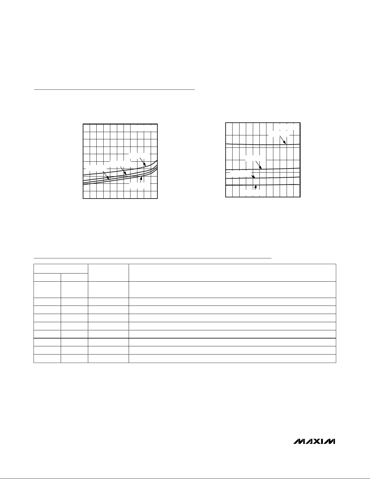
Typical Operating Characteristics
(TA = +25°C, unless otherwise noted.)
0
20
10
40
30
50
60
-40 -10 5 20-25 35 50 65 80 95 110 125
SUPPLY CURRENT vs. TEMPERATURE
MAX7319 toc02
TEMPERATURE (°C)
SUPPLY CURRENT (μA)
V+ = +3.3V
V+ = +5.0V
V+ = +1.71V
V+ = +2.5V
f
SCL
= 400kHz
Pin Description
STANDBY CURRENT vs. TEMPERATURE
2.0
1.8
1.6
1.4
1.2
1.0
0.8
0.6
STANDBY CURRENT (μA)
0.4
0.2
0
V+ = +2.5V
-40 -10 5-25 20 35 50 65 80 95 110 125
V+ = +3.3V
TEMPERATURE (°C)
f
= 0kHz
SCL
V+ = +5.0V
V+ = +1.71V
MAX7319 toc01
PIN
QSOP TQFN
1, 3 15, 1 AD0, AD2
216 RST Reset Input, Active Low. Drive RST low to clear the 2-wire interface.
4–7, 9–12 2–5, 7–10 I0–I7 Input Ports. I0 to I7 are CMOS logic inputs protected to +6V.
8 6 GND Ground
13 11 INT Interrupt Output, Active Low. INT is an open-drain output rated at +6V.
14 12 SCL I2C-Compatible Serial Clock Input
15 13 SDA I2C-Compatible Serial Data I/O
16 14 V+ Positive Supply Voltage. Bypass V+ to GND with a ceramic capacitor of at least 0.047µF.
— EP EP Exposed Pad. Connect exposed pad to GND.
NAME FUNCTION
Address Inputs. Select device slave address with AD0 and AD2. Connect AD0 and AD2
to either GND, V+, SCL, or SDA to give four logic combinations (see Table 3).
Page 5
Detailed Description
MAX7319–MAX7329 Family Comparison
The MAX7319–MAX7323 family consists of five pincompatible, eight-port expanders. Each version is optimized for different applications. The MAX7328 and
MAX7329 are second sources to the PCF8574 and
PCF8574A.
The MAX7324–MAX7327 family consists of four pincompatible, 16-port expanders that integrate the functions of the MAX7320 and one of either the MAX7319,
MAX7321, MAX7322, or MAX7323.
Functional Overview
The MAX7319 is a general-purpose port expander,
operating from a +1.71V to +5.5V supply that provides
eight CMOS input ports that are overvoltage protected
to +6V independent of supply voltage.
The MAX7319 is set to one of 16 I2C slave addresses
(0x60 to 0x6F) using the address-select inputs AD2
and AD0, and is accessed over an I
2
C serial interface.
The RST input clears the serial interface in case of a
hung bus, terminating any serial transaction to or from
the MAX7319.
The input ports offer latching transition detection functionality. All input ports are continuously monitored for
MAX7319
I2C Port Expander with Eight Inputs and
Maskable Transition Detection
_______________________________________________________________________________________ 5
Table 1. MAX7319–MAX7329 Family Comparison
2
C
I
PART
8-PORT EXPANDERS
MAX7319 110xxxx 8 Yes — —
MAX7320 101xxxx — — — 8
MAX7321 110xxxx Up to 8 — Up to 8 —
MAX7322 110xxxx 4 Yes — 4
SLAVE
ADDRESS
INPUTS
INPUT
INTERRUPT
MASK
OPENDRAIN
OUTPUTS
PUSH-
PULL
OUTPUTS
APPLICATION
Input-only versions:
Eight input ports with programmable latching
transition detection interrupt and selectable pullups.
Offers maximum versatility for automatic input
monitoring. An interrupt mask selects which inputs
cause an interrupt on transitions, and transition flags
identify which inputs have changed (even
momentarily) since the ports were last read.
Output-only versions:
Eight push-pull outputs with selectable power-up
default levels.
Push-pull outputs offer faster rise time than opendrain outputs, and require no pullup resistors.
I/O versions:
Eight open-drain I/O ports with latching transition
detection interrupt and selectable pullups.
Open-drain outputs can level shift the logic-high
state to a higher or lower voltage than V+ using
external pullup resistors. Any port can be used as an
input by setting the open-drain output to logic-high.
Transition flags identify which inputs have changed
(even momentarily) since the ports were last read.
Four input-only, four output-only versions:
Four input ports with programmable latching
transition detection interrupt and selectable pullups.
Four push-pull outputs with selectable power-up
default levels.
Page 6

MAX7319
changes. An input change sets one of eight flag bits
that identify changed input(s). All flags are cleared
upon a subsequent read or write transaction to the
MAX7319.
A latching interrupt output, INT, is programmed to flag
input data changes on input ports through an interrupt
mask register. By default, data changes on any input
port force INT to a logic-low. The interrupt output, INT,
and all transition flags are cleared when the MAX7319
is next accessed through the serial interface.
Internal pullup resistors to V+ are selected by the
address-select inputs, AD0 and AD2. Pullups are
enabled on the input ports in groups of four (see Table 3).
Initial Power-Up
On power-up, the transition detection logic is reset, and
INT is released to a high-impedance state. The interrupt mask register is set to 0xFF, enabling the interrupt
output for transitions on all eight input ports. The transition flags are cleared to indicate no data changes.
RST Input
The RST input voids any I2C transaction involving the
MAX7319, forcing the MAX7319 into the I2C STOP condition. A reset does not affect the interrupt output (INT)
or change the contents of the interrupt mask register.
RST is overvoltage tolerant to +6V.
Standby Mode
When the serial interface is idle, the MAX7319 automatically enters standby mode, drawing minimal supply
current.
Slave Address and Input Pullup Selection
Address inputs AD0 and AD2 determine the MAX7319
slave address and select which inputs have pullup
resistors. Pullups are enabled on the input ports in
groups of four (see Table 3). The MAX7319, MAX7321,
MAX7322, and MAX7323 use a different range of slave
addresses (110xxxx) than the MAX7320 (101xxxx).
The MAX7319 slave address is determined on each I2C
transmission, regardless of whether the transmission is
actually addressing the MAX7319. The MAX7319 distinguishes whether address inputs AD2 and AD0 are connected to SDA or SCL instead of fixed logic levels V+
or GND during this transmission. This means that the
MAX7319 slave address can be configured dynamically
in the application without cycling the device supply.
On initial power-up, the MAX7319 cannot decode the
address inputs AD2 and AD0 fully until the first I
2
C
transmission. AD0 and AD2 initially appear to be connected to V+ or GND. This is important because the
address selection determines which inputs have
pullups applied. However, at power-up, the I2C SDA
and SCL bus interface lines are high impedance at the
pins of every device (master or slave) connected to the
bus, including the MAX7319. This is guaranteed as part
I2C Port Expander with Eight Inputs and
Maskable Transition Detection
6 _______________________________________________________________________________________
Table 1. MAX7319–MAX7329 Family Comparison (continued)
2
C
I
PART
MAX7323 110xxxx Up to 4 — Up to 4 4
SLAVE
ADDRESS
INPUTS
MAX7328
MAX7329
16-PORT EXPANDERS
MAX7324 8 Yes — 8 Software equivalent to a MAX7320 plus a MAX7321.
MAX7325 Up to 8 — Up to 8 8 Software equivalent to a MAX7320 plus a MAX7319.
MAX7326 4 Yes — 12 Software equivalent to a MAX7320 plus a MAX7322.
MAX7327
0100xxx
0111xxx
101xxxx
and
110xxxx
Up to 8 — Up to 8 —
Up to 4 — Up to 4 12 Software equivalent to a MAX7320 plus a MAX7323.
INPUT
INTERRUPT
MASK
OPENDRAIN
OUTPUTS
PUSH-
PULL
OUTPUTS
Four I/O, four output-only versions:
Four open-drain I/O ports with latching transition
detection interrupt and selectable pullups.
Four push-pull outputs with selectable power-up
default levels.
PCF8574-, PCF8574A-compatible versions:
Eight open-drain I/O ports with nonlatching transition
detection interrupt and pullups on all ports.
All ports power up as inputs (or logic-high outputs).
Any port can be used as an input by setting the
open-drain output to logic-high.
APPLICATION
Page 7
of the I2C specification. Therefore, address inputs AD2
and AD0 that are connected to SDA or SCL normally
appear at power-up to be connected to V+. The pullup
selection logic uses AD0 to select whether pullups are
enabled for ports I3–I0, and uses AD2 to select whether
pullups are enabled for ports I7–I4. The rule is that a
logic-high SDA or SCL connection selects the pullups,
while a logic-low deselects the pullups (Table 3). The
pullup configuration is correct on power-up for a standard I2C configuration, where SDA and SCL are pulled
up to V+ by the external I2C pullup resistors.
There are circumstances where the assumption that
SDA = SCL = V+ on power-up is not true, for example,
in true hot-swap applications, in which there is legitimate bus activity during power-up. Also, if SDA and
SCL are terminated with pullup resistors to a different
supply voltage than the MAX7319’s supply voltage, and
if that pullup supply rises later than the MAX7319’s supply, then SDA or SCL may appear at power-up to be
connected to GND. In such applications, use the four
address combinations that are selected by connecting
address inputs AD2 and AD0 to V+ or GND (shown in
bold in Table 3). These selections are guaranteed to be
correct at power-up, independent of SDA and SCL
behavior. If one of the other 12 address combinations is
used, be aware that an unexpected combination of
pullups might be asserted until the first I2C transmission (to any device, not necessarily the MAX7319) is
put on the bus.
Port Inputs
Port inputs switch at CMOS logic levels as determined
by the expander’s supply voltage, and are overvoltage
tolerant to +6V, independent of the expander’s supply
voltage.
Port-Input Transition Detection
All eight input ports are monitored for changes since
the expander was last accessed through the serial
interface. The state of the input ports is stored in an
internal “snapshot” register for transition monitoring.
The snapshot is continuously compared with the actual
input conditions, and if a change is detected for any
port input, an internal transition flag is set for that port.
The eight port inputs are sampled (internally latched
into the snapshot register) and the old transition flags
cleared during the I2C acknowledge of every MAX7319
read and write access. The previous port transition
flags are read through the serial interface as the second byte of a 2-byte read sequence.
MAX7319
I2C Port Expander with Eight Inputs and
Maskable Transition Detection
_______________________________________________________________________________________ 7
Table 2. Read and Write Access to Eight-Port Expander Family
2
I
PART
MAX7319 110xxxx 8 Yes — —
MAX7320 101xxxx — — — 8
MAX7321 110xxxx Up to 8 — Up to 8 —
MAX7322 110xxxx 4 Yes — 4
MAX7323 110xxxx Up to 4 — Up to 4 4 <port outputs>
MAX7328 0100xxx Up to 8 — Up to 8 —
MAX7329 0111xxx Up to 8 — Up to 8 —
C SLAVE
ADDRESS
INPUTS
INTERRUPT
MASK
OPENDRAIN
OUTPUTS
PUSH-
PULL
OUTPUTS
2
C DATA WRITE I2C DATA READ
I
<I7–I0 interrupt
mask>
<O7–O0 port
outputs>
<P7–P0 port
outputs>
<O7, O6 outputs,
I5–I2 interrupt
mask, O1, O0
outputs>
<P7–P0 port
outputs>
<P7–P0 port
outputs>
<I7–I0 port inputs>
<I7–I0 transition flags>
<O7–O0 port inputs>
<P7–P0 port inputs>
<P7–P0 transition flags>
<O7, O6, I5–I2, O1, O0 port
inputs>
<0, 0, I5–I2 transition flags,
0, 0>
<O7, O6, P5–P2, O1, O0 port
inputs>
<0, 0, P5–P2 transition flags,
0, 0>
<P7–P0 port inputs>
<P7–P0 port inputs>
Page 8

MAX7319
A long read sequence (more than 2 bytes) can be used
to poll the expander continuously without the overhead
of resending the slave address. If more than 2 bytes
are read from the expander, the expander repeatedly
returns the input port data followed by the transition
flags. The inputs are repeatedly resampled and the
transition flags repeatedly reset for each pair of bytes
read. All changes that occur during a long read sequence
are detected and reported.
The MAX7319 includes an 8-bit interrupt mask register
that selects which inputs generate an interrupt upon
change. Each input’s transition flag is set when its input
changes, independent of the interrupt mask register
settings. The interrupt mask register allows the processor to be interrupted for critical events, while the inputs
and the transition flags can be polled periodically to
detect less critical events.
The INT logic ensures that unnecessary interrupts are
not asserted, yet data transitions are detected and
reported regardless of when the transition occurs. The
INT output is not reasserted during a read sequence to
avoid recursive reentry into an interrupt service routine.
If transition occurs during read sequence, the INT
assertion is delayed until the STOP condition, however,
INT is not reasserted upon a STOP condition if the
changed input data is read before the STOP occurs.
Transition-Detection Masks
The transition-detection logic incorporates a transition
flag and an interrupt mask bit for each input port. The
eight change flags can be read through the serial interface, and the 8-bit interrupt mask is set through the serial interface.
Each port’s transition flag is set when that port’s input
changes, and the transition flag remains set even if the
input returns to its original state. The port’s interrupt
mask determines whether a transition on that input port
generates an interrupt. Enable interrupts for high-priority inputs using the interrupt mask. The interrupt allows
the system to respond quickly to changes on these
inputs. Poll the MAX7319 periodically to monitor lessimportant inputs. The transition flags indicate whether a
permanent or transient change has occurred on any
input since the MAX7319 was last accessed.
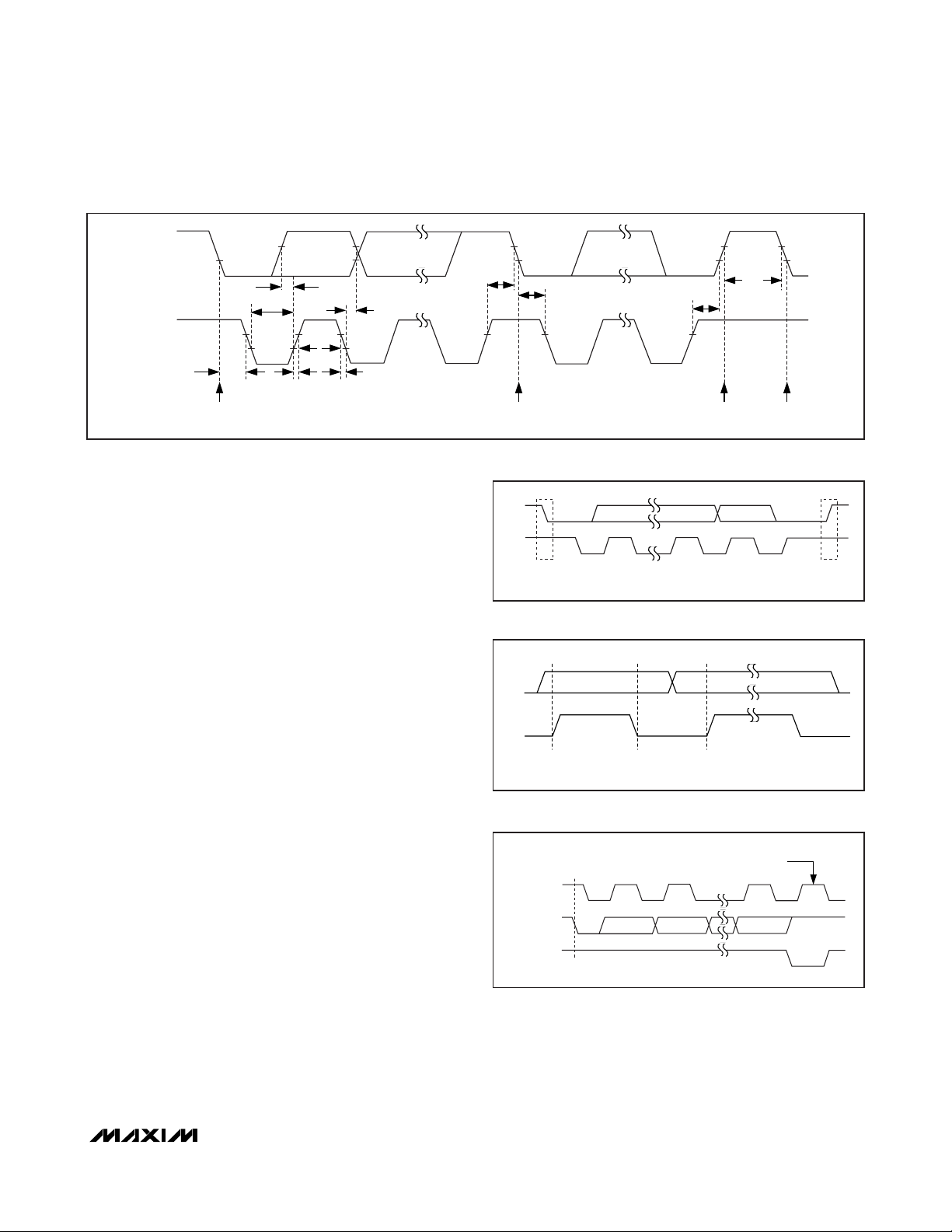
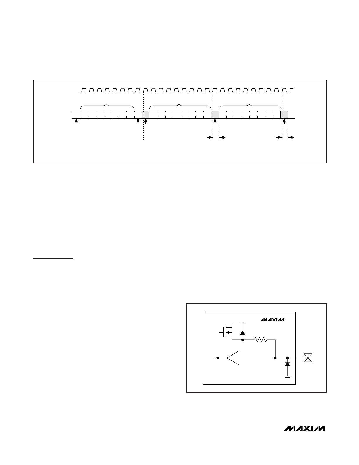
Serial Interface
Serial Addressing
The MAX7319 operates as a slave that sends and
receives data through an I2C interface. The interface
uses a serial data line (SDA) and a serial clock line (SCL)
to achieve bidirectional communication between master(s) and slave(s). The master initiates all data transfers
to and from the MAX7319 and generates the SCL clock
that synchronizes the data transfer (Figure 1).
I2C Port Expander with Eight Inputs and
Maskable Transition Detection
8 _______________________________________________________________________________________
Table 3. MAX7319 Address Map
PIN CONNECTION DEVICE ADDRESS 40kΩ INPUT PULLUP ENABLED
AD2 AD0 A6 A5 A4 A3 A2 A1 A0 I7 I6 I5 I4 I3 I2 I1 I0
SCL GND 1100000YYYY————
SCL V+ 1100001YYYYYYYY
SCL SCL 1 1 0 0 0 1 0 Y Y Y Y Y Y Y Y
SCL SDA 1 1 0 0 0 1 1 Y Y Y Y Y Y Y Y
SDA GND 1100100YYYY————
SDA V+ 1100101YYYYYYYY
SDA SCL 1 1 0 0 1 1 0 Y Y Y Y Y Y Y Y
SDA SDA 1 1 0 0 1 1 1 Y Y Y Y Y Y Y Y
GND GND 1 1 0 1 0 0 0 — — — — — — — —
GND V+ 1101001————YYYY
GND SCL 1101010————YYYY
GND SDA 1101011————YYYY
V+ GND 1101100YYYY————
V+ V+ 1101101YYYYYYYY
V+ SCL 1101110YYYYYYYY
V+ SDA 1101111YYYYYYYY
Page 9
SDA operates as both an input and an open-drain output. A pullup resistor, typically 4.7kΩ, is required on
SDA. SCL operates only as an input. A pullup resistor,
typically 4.7kΩ, is required on SCL if there are multiple
masters on the 2-wire interface, or if the master in a single-master system has an open-drain SCL output.
Each transmission consists of a START condition sent
by a master, followed by the MAX7319’s 7-bit slave
address plus R/W bit, then 1 or more data bytes, and
finally a STOP condition (Figure 2).
START and STOP Conditions
Both SCL and SDA remain high when the interface is
not busy. A master signals the beginning of a transmission with a START (S) condition by transitioning SDA
from high to low while SCL is high. When the master
has finished communicating with the slave, the master
issues a STOP (P) condition by transitioning SDA from
low to high while SCL is high. The bus is then free for
another transmission (Figure 2).
Bit Transfer
One data bit is transferred during each clock pulse.
The data on SDA must remain stable while SCL is high
(Figure 3).
Acknowledge
The acknowledge bit is a clocked 9th bit the recipient
uses to acknowledge receipt of each byte of data
(Figure 4). Each byte transferred effectively requires 9
bits. The master generates the 9th clock pulse, and the
recipient pulls down SDA during the acknowledge
clock pulse, so the SDA line is stable low during the
high period of the clock pulse. When the master is
transmitting to the MAX7319, the MAX7319 generates
the acknowledge bit because the device is the recipient.
When the MAX7319 is transmitting to the master, the
master generates the acknowledge bit because the
master is the recipient.
MAX7319
I2C Port Expander with Eight Inputs and
Maskable Transition Detection
_______________________________________________________________________________________ 9
Figure 1. 2-Wire Serial-Interface Timing Details
Figure 2. START and STOP Conditions
Figure 3. Bit Transfer
Figure 4. Acknowledge
SDA
t
SU,DAT
t
LOW
SCL
t
HD,STA
START CONDITION
t
HIGH
t
R
t
HD,DAT
t
F
t
SU,STA
REPEATED START CONDITION
t
HD,STA
SDA
SCL
SP
START
CONDITION
t
SU,STO
STOP
CONDITION
t
BUF
START
CONDITION
STOP
CONDITION
SDA
SCL
DATA LINE STABLE;
DATA VALID
CHANGE OF DATA
ALLOWED
CLOCK PULSE
FOR ACKNOWLEDGMENT
SCL
SDA BY
TRANSMITTER
SDA BY
RECEIVER
START
CONDITION
S
12 89
Page 10
MAX7319
Slave Address
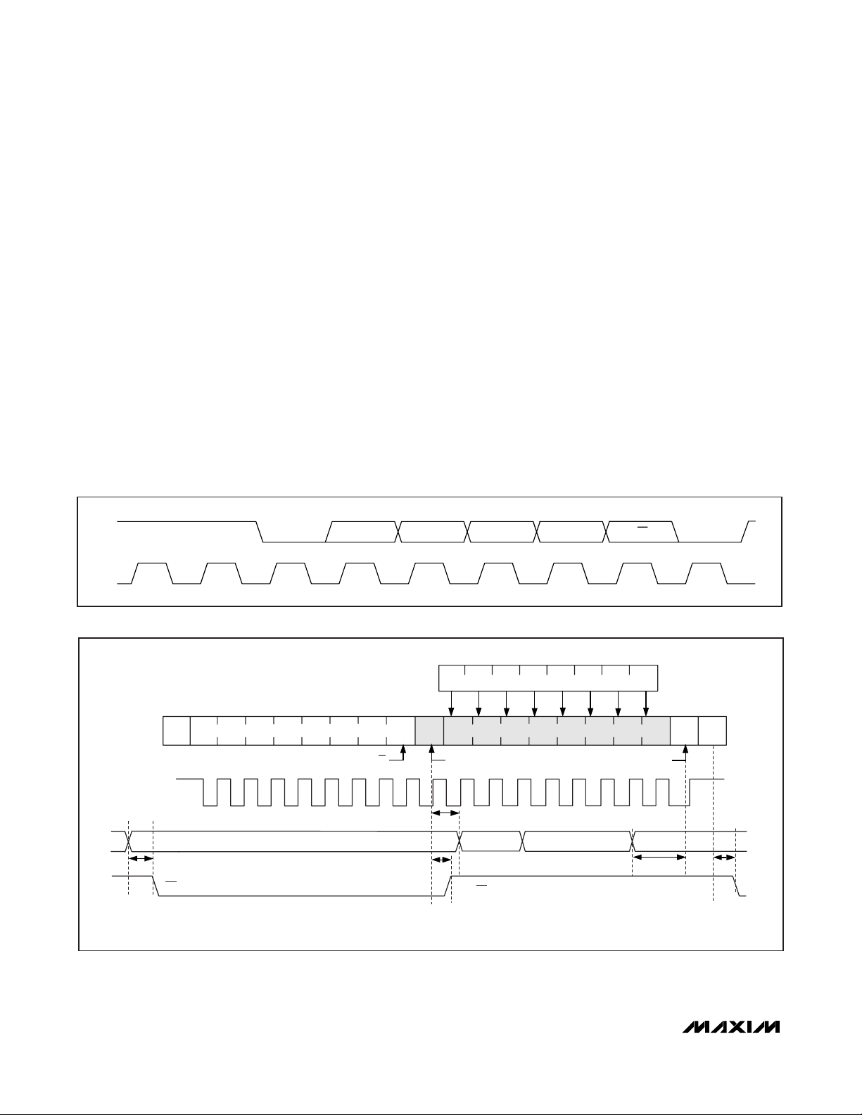
The MAX7319 has a 7-bit slave address (Figure 5). The
8th bit following the 7-bit slave address is the R/W bit. It
is low for a write command, and high for a read command.
The 1st (A6), 2nd (A5), and 3rd (A4) bits of the MAX7319
slave address are always 1, 1, and 0. Connect AD2 and
AD0 to GND, V+,SDA, or SCL to select slave address
bits A3, A2, A1, and A0. The MAX7319 has 16 possible
slave addresses (Table 3), allowing up to 16 MAX7319
devices on an I
2
C bus
Accessing the MAX7319
I2C-interface access to the MAX7319 is summarized as
follows (Table 2).
A single-byte read from the MAX7319 returns the sta-
tus of the eight input ports, and clears both the internal
transition flags and the INT output (Figure 7).
A 2-byte read returns the status of the eight input ports
(as for a single-byte read), followed by the transition
flags. The internal transition flags and the INT output
are cleared when the MAX7319 acknowledges the
slave address byte, but the previous transition flag data
is sent as the second byte (Figure 8).
A multibyte read (more than 2 bytes before the I
2
C
STOP bit) repeatedly returns the input port data, alternating with the transition flags. As the input data is
resampled for each transmission, and the transition
flags are reset each time, a multibyte read continuously
returns the current data and identifies any changing
input ports.
If a port input data change occurs during the read
sequence, INT is reasserted after the I
2
C STOP bit. The
MAX7319 does not generate another interrupt during a
single-byte or multibyte read.
I2C Port Expander with Eight Inputs and
Maskable Transition Detection
10 ______________________________________________________________________________________
Figure 5. Slave Address
Figure 6. Reading from the MAX7319 (1 Data Byte)
S = START CONDITION SHADED = SLAVE TRANSMISSION
P = STOP CONDITION N = NOT ACKNOWLEDGE
.
SDA
SCL
11
MSB
0
A3
A2 A1 A0
LSB
R/W
ACK
S1 1 0 A
SCL
PORT INPUT
t
IV
INT OUTPUT
MAX7319 SLAVE ADDRESS
R/W
PORT INPUTS
I6
I7
1
PORT SNAPSHOT
t
PH
t
IR
INT REMAINS HIGH UNTIL STOP CONDITION
I1
I2I3I4I5
PORT SNAPSHOT
I0
P
N
D0D1D2D3D4D5D6D7
t
PSU
t
IP
Page 11

MAX7319
I2C Port Expander with Eight Inputs and
Maskable Transition Detection
______________________________________________________________________________________ 11
Figure 7. Reading from the MAX7319 (2 Data Bytes)
Input port data is sampled during the preceding I2C
acknowledge bit (the acknowledge bit for the I2C slave
address in the case of a single-byte or 2-byte read).
A single-byte write to the MAX7319 sets the interrupt
mask register, and clears both the internal transition
flags and the INT output.
A multibyte write to the MAX7319 sets the interrupt
mask register repeatedly.
Reading from the MAX7319
A read from the MAX7319 starts with the master transmitting the MAX7319’s slave address with the R/W bit
set high. The MAX7319 acknowledges the slave
address and samples the input ports during acknowledge bit. INT deasserts during the slave address
acknowledge.
Typically, the master reads 1 or 2 bytes from the
MAX7319, with each byte, except the last one, being
acknowledged by the master upon reception.
When the master reads 1 byte from the MAX7319 and
subsequently issues a STOP condition (Figure 6), the
MAX7319 transmits the current port data, clears the
transition flags, and resets the transition detection. INT
deasserts during the slave address acknowledge. The
new snapshot data is the current port data transmitted
to the master; therefore, port transitions ocurring during
the transmission are detected. INT remains high until
the STOP condition.
When the master reads 2 bytes from the MAX7319 and
subsequently issues a STOP condition (Figure 7), the
MAX7319 transmits the current port data, followed by
the transition flags. The transition flags are cleared, and
transition detection reset. INT deasserts during the
slave address acknowledge. The new snapshot data is
the current port data transmitted to the master; therefore, port transitions occurring during the transmission
are detected. INT remains high until the STOP condition. When the master reads more than 2 bytes, the
input port data alternates with the transition flag.
S = START CONDITION SHADED = SLAVE TRANSMISSION
P = STOP CONDITION N = NOT ACKNOWLEDGE
I6
I7
SGALF TPURRETNISTUPNI TROP
I1
I2I3I4I5
I0
F6
F7
F1
F2F3F4F5
F0
MAX7319 SLAVE ADDRESS A011S P1
R/W
SCL
PORTS
t
IV
INT OUTPUT
PORT SNAPSHOT
t
PH
t
IR
INT REMAINS HIGH UNTIL STOP CONDITION
PORT SNAPSHOT
S = START CONDITION SHADED = SLAVE TRANSMISSION
P = STOP CONDITION N = NOT ACKNOWLEDGE
A
D0D1D2D3D4D5D6D7
D7 D6 D5 D4 D3 D2 D1 D0 N
t
PSU
PORT SNAPSHOT
t
IP
Page 12
Writing to the MAX7319
A write to the MAX7319 starts with the master transmitting the MAX7319’s slave address with the R/W bit set
low. The MAX7319 acknowledges the slave address,
and samples the input ports during the acknowledge
bit. INT deasserts during the slave address acknowledge. The master can now transmit 1 or more bytes of
data. The MAX7319 acknowledges these subsequent
bytes of data and updates the interrupt mask register
with each new byte until the master issues a STOP condition (Figure 8).
Applications Information
Port Input and I2C Interface Level
Translation from Higher or Lower
Logic Voltages
The MAX7319 I2C interface (SDA, SCL, AD0, AD2),
reset input RST, interrupt output INT, and the eight
input ports I0–I7 are overvoltage protected to +6V independent of V+. This allows the MAX7319 to operate
from a lower supply voltage, such as +3.3V, while the
I2C interface and/or any of the eight input ports are driven from a higher logic level, such as +5V.
The MAX7319 can operate from a higher supply voltage, such as +3V, while the I2C interface and/or some
of the input ports I0–I7 are driven from a lower logic
level, such as +2.5V. Apply a minimum voltage of 0.7 x
V+ to assert a logic-high on any input. For example, a
MAX7319 operating from a +5V supply may not recognize a +3.3V nominal logic-high. One solution for input
level translation is to drive the MAX7319 inputs from
open-drain outputs. Use a pullup resistor to V+ or a
higher supply to ensure a high logic voltage of greater
than 0.7 x V+.
Hot Insertion
RST, SCL, SDA, AD0, and AD2 remain high impedance
with up to +6V asserted on them when the MAX7319 is
powered down (V+ = 0). The MAX7319 can therefore
be used in hot-swap applications.
Each of the input ports I0–I7 has a protection diode to
GND (Figure 9). When a port input is driven to a voltage
lower than GND, the protection diode clamps the voltage to a diode drop below GND.
Each of the input ports I0–I7 also has a 40kΩ (typ)
pullup resistor that can be enabled or disabled. When a
port input is driven to a voltage higher than V+,the
body diode of the pullup enable switch conducts and
the 40kΩ pullup resistor is enabled. When the
MAX7319 is powered down (V+ = 0), every input port
appears as a 40kΩ resistor in series with a diode connected to GND. Input ports are protected to +6V under
any of these circumstances (Figure 9).
MAX7319
I2C Port Expander with Eight Inputs and
Maskable Transition Detection
12 ______________________________________________________________________________________
Figure 9. Input Port Structure
Figure 8. Writing to the MAX7319
S = START CONDITION SHADED = SLAVE TRANSMISSION
P = STOP CONDITION N = NOT ACKNOWLEDGE
SCL
SDA
12345678
SLAVE ADDRESS
S0
START CONDITION R/W
AAA
DATA TO INTERRUPT MASK DATA TO INTERRUPT MASK
DATA 1 DATA 2
t
PV
V+
V+
PULLUP
ENABLE
INPUT
P
MAX7319
40kΩ
t
PV
I0–I7
Page 13

MAX7319
I2C Port Expander with Eight Inputs and
Maskable Transition Detection
______________________________________________________________________________________ 13
Power-Supply Considerations
The MAX7319 operates with a +1.71V to +5.5V supply
voltage over the -40°C to +125°C temperature range.
Bypass V+ to GND with a ceramic capacitor of at least
0.047µF as close to the device as possible. For the
TQFN version, connect the exposed pad to GND.
Compatibility with MAX6965, MAX7315,
and MAX7316
The MAX7319 is subset pin compatible with the
MAX6965, MAX7315, and MAX7316. The pin differences are shown in Table 4. The MAX7319 is not software compatible with MAX6965, MAX7315, or
MAX7316. In many cases, it is possible to design a PC
board to work with all these port expanders, providing
design flexibility.
Table 4. MAX7319, MAX6965, MAX7315,
and MAX7316 Pin Compatibility
Pin Configurations
MAX7319
I2
I7
I6
I5
I4
V+
3.3V
47nF
μC
SCL
SDA
SCL
AD0
I1
I0
SDA
I3
GND
INPUT 3
INPUT 2
AD2
INT
INPUT 1
INPUT 0
INPUT 7
INPUT 6
INPUT 5
INPUT 4
RST
INT
RST
Typical Application Circuit
I7
TOP VIEW
SDA
AD0
RST
SCL
12 10 9
11
13
14
V+
+
MAX7319
* EP
15
16
I6
I5
8
I4
7
GND
6
I3
5
PIN-PACKAGE PIN FUNCTION
16
QSOP16TQFN
MAX7319 MAX7315
MAX6965 AND
MAX7316
1 15 AD0 AD0 BLINK
216RST AD1 RST
3 1 AD2 AD2 AD0
13
2
I0 INT
AD2
TQFN
3mm x 3mm
* EXPOSED PAD CONNECTED TO GND.
AD0
AD2
GND
+
1
2
RST
3
MAX7319
4
I0
I1
5
I2
6
I3
7
8
QSOP
I1
4
I2
16
15
14
13
12
11
10
9
V+
SDA
SCL
INT
I7
I6
I5
I4
Page 14

MAX7319
I2C Port Expander with Eight Inputs and
Maskable Transition Detection
14 ______________________________________________________________________________________
Chip Information
PROCESS: BiCMOS
CONNECT EXPOSED PAD TO GND
Functional Diagram
AD0
AD2
SCL
SDA
RST
INPUT
FILTER
POWER-ON
RESET
I2C
CONTROL
MAX7319
INPUT
PORTS
I7
I6
I5
I4
I3
I2
I1
I0
INT
Page 15

MAX7319
I2C Port Expander with Eight Inputs and
Maskable Transition Detection
______________________________________________________________________________________ 15
Package Information
(The package drawing(s) in this data sheet may not reflect the most current specifications. For the latest package outline information,
go to www.maxim-ic.com/packages
.)
MARKING
E/2
D/2
D
0.10 C 0.08 C
E
AAAA
C
L
(NE - 1) X e
(ND - 1) X e
C
L
A
A2
A1
L
e
k
L
E2
C
L
e
PACKAGE OUTLINE
8, 12, 16L THIN QFN, 3x3x0.8mm
D2/2
D2
b
E2/2
0.10 M C A B
C
L
L
e
21-0136
12x16L QFN THIN.EPS
1
I
2
8L 3x3
PKG
REF. MIN.
MIN.
NOM. MAX.
0.70 0.75 0.80
A
b
0.25 0.30 0.35
D
2.90
3.00 3.10
E
2.90 3.00 3.10
e
0.65 BSC.
L
0.35
0.55 0.75
ND
NE
0
0.02
A1
A2
0.20 REF
0.25
k
NOTES:
1. DIMENSIONING & TOLERANCING CONFORM TO ASME Y14.5M-1994.
2. ALL DIMENSIONS ARE IN MILLIMETERS. ANGLES ARE IN DEGREES.
3. N IS THE TOTAL NUMBER OF T ERMINALS.
4. THE TERMINAL #1 IDENTIFIER AND TERMINAL NUMBERING CONVENTION SHALL CONFORM TO
JESD 95-1 SPP-012. DETAILS OF TERMINAL #1 IDENTIFIER ARE OPTIONAL, BUT MUST BE LOCATED
WITHIN THE ZONE INDICATED. THE TERMINAL #1 IDENTIFIER MAY BE EITHER A MOLD OR
MARKED FEATURE.
5. DIMENSION b APPLIES TO METALLIZED TERMINAL AND IS MEASURED BETWEEN 0.20 mm AND 0.25 mm
FROM TERMINAL TIP.
6. ND AND NE REFER TO THE NUMBER OF TERMINALS ON EACH D AND E SIDE RESPECTIVELY.
7. DEPOPULATION IS POSSIBLE IN A SYMMETRICAL FASHION.
8. COPLANARITY APPLIES TO THE EXPOSED HEAT SINK SLUG AS WELL AS THE TERMINALS .
9. DRAWING CONFORMS TO JEDEC MO220 REVISION C.
10. MARKING IS FOR PACKAGE ORIENTATION REFERENCE ONLY.
11. NUMBER OF LEADS SHOWN ARE FOR REFERENCE ONLY.
12. WARPAGE NOT TO EXCEED 0.10mm.
12L 3x3
NOM. MAX. NOM.
0.70
0.75
0.20
0.25
2.90
3.00
2.90
3.00
0.50 BSC.
0.45
8
2
2
-
0.55
12N
0.05
0.0230.05
0
0.20 REF
-
0.25
3
-
0.80
0.30
3.10
3.10
0.65
-
16L 3x3
MIN. MAX.
0.70
0.75
0.20
0.25
2.90
3.00
2.90
3.00
0.50 BSC.
0.30
0.40
16
4
040.02
0.20 REF
-
0.25
EXPOSED PAD VARIATIONS
PKG.
0.80
0.30
3.10
3.10
0.50
0.05
CODES
TQ833-1 1.250.25 0.70 0.35 x 45° WEEC1.250.700.25
T1233-1
T1233-3
T1233-4
T1633-2 0.95
T1633F-3
T1633FH-3 0.65 0.80 0.95
T1633-4 0.95
T1633-5 0.95
-
D2
MIN.
NOM.
0.95
1.10
1.10
0.95
1.10
0.65
0.80
1.10 1.25 0.95 1.10
1.10
MAX.
1.25
1.25
1.251.10
1.25
0.95
1.25
E2
NOM.
MIN.
MAX.
1.10
0.95
1.25
0.95 1.10 0.35 x 45°1.25 WEED-10.95
1.100.95
1.10
1.25
0.95
0.80
0.95
0.65
0.95
0.65 0.80
1.25
1.10 1.25
0.95
PACKAGE OUTLINE
8, 12, 16L THIN QFN, 3x3x0.8mm
PIN ID
JEDEC
WEED-1
0.35 x 45°
WEED-11.25
0.35 x 45°
0.35 x 45°
WEED-2
0.225 x 45°
WEED-2
0.225 x 45°
WEED-2
0.35 x 45°
WEED-2
0.35 x 45° WEED-2
21-0136
2
I
2
Page 16

MAX7319
I2C Port Expander with Eight Inputs and
Maskable Transition Detection
Maxim cannot assume responsibility for use of any circuitry other than circuitry entirely embodied in a Maxim product. No circuit patent licenses are
implied. Maxim reserves the right to change the circuitry and specifications without notice at any time.
16 ____________________Maxim Integrated Products, 120 San Gabriel Drive, Sunnyvale, CA 94086 408-737-7600
© 2005 Maxim Integrated Products Printed USA is a registered trademark of Maxim Integrated Products, Inc.
Package Information (continued)
(The package drawing(s) in this data sheet may not reflect the most current specifications. For the latest package outline information,
go to www.maxim-ic.com/packages
.)
QSOP.EPS
 Loading...