

Page 1
现货库存、技术资料、百科信息、热点资讯,精彩尽在鼎好!
MAX7310
2-Wire-Interfaced 8-Bit I/O Port Expander
with Reset
________________________________________________________________ Maxim Integrated Products 1
19-2698; Rev 3; 2/05
For pricing, delivery, and ordering information, please contact Maxim/Dallas Direct! at
1-888-629-4642, or visit Maxim’s website at www.maxim-ic.com.
General Description
The MAX7310 provides 8-bit parallel input/output port
expansion for SMBus™-compatible and I2C™-compatible applications. The MAX7310 consists of an input port
register, an output port register, a polarity inversion register, a configuration register, a bus timeout register,
and an SMBus/I
2
C-compatible serial interface. The system master can invert the MAX7310 input data by writing to the active-high polarity inversion register. The
system master can enable or disable bus timeout by
writing to the bus timeout register.
Any of the eight I/O ports may be configured as input or
output. An active-low reset input sets the eight I/Os as
inputs. Three address select pins configure one of 56
slave ID addresses.
The MAX7310 is available in 16-pin thin QFN, TSSOP,
and QSOP packages and is specified over the -40°C to
+125°C automotive temperature range.
Applications
Servers
RAID Systems
Industrial Control
Medical Equipment
Instrumentation, Test Measurement
Features
♦ 400kHz 2-Wire Interface
♦ 2.3V to 5.5V Operation
♦ Low Standby Current (1.7µA typ)
♦ Bus Timeout for Lock-Up-Free Operation
♦ 56 Slave ID Addresses
♦ Polarity Inversion
♦ Eight I/O Pins that Default to Inputs on Power-Up
♦ 5V Tolerant Open-Drain Output on I/O0
♦ 4mm x 4mm, 0.8mm Thin QFN Package
♦ -40°C to +125°C Operation
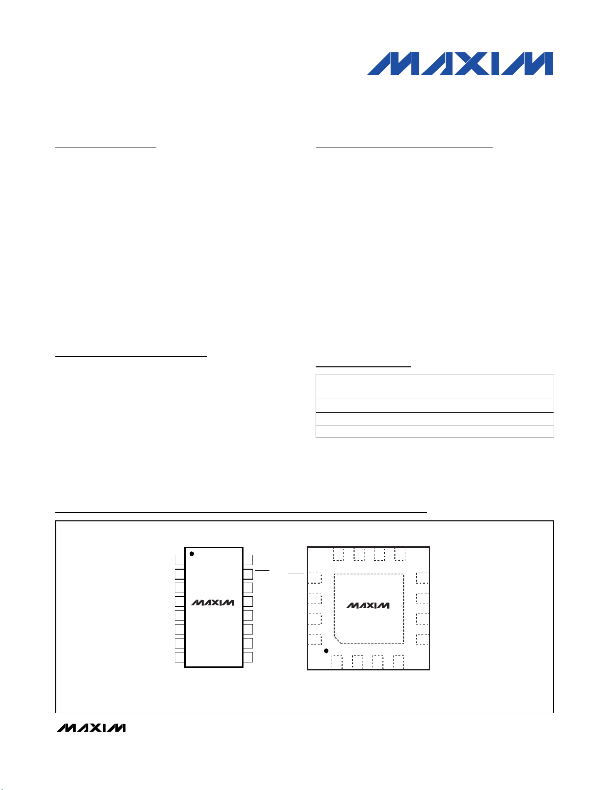
Ordering Information
Pin Configurations
SMBus is a trademark of Intel Corp.
Purchase of I
2
C components of Maxim Integrated Products, Inc.,
or one of its sublicensed Associated Companies, conveys a
license under the Philips I
2
C Patent Rights to use these compo-
nents in an I
2
C system, provided that the system conforms to the
I
2
C Standard Specification as defined by Philips.
PART TEMP RANGE
MAX7310AUE -40°C to +125°C 16 TSSOP —
MAX7310AEE -40°C to +125°C 16 QSOP —
MAX7310ATE -40°C to +125°C 16 Thin QFN T1644-4
PINPACKAGE
PKG
CODE
TOP VIEW
SCL
SDA
AD0
AD1
AD2
I/O0
I/O1
GND
1
2
3
4
5
6
7
8
MAX7310
TSSOP/QSOP
V+
16
RESET
15
I/O7
14
I/O6
13
I/O5
12
11
I/O4
I/O3
10
9
I/O2
RESET
V+
SCL
SDA
I/O7
12
11 10 9
13
14
15
16
MAX7310ATE
1234
AD0
AD1
THIN QFN
I/O6
I/O5
AD2
I/O4
I/O0
I/O3
8
I/O2
7
GND
6
I/O1
5
Page 2
MAX7310
2-Wire-Interfaced 8-Bit I/O Port Expander
with Reset
2 _______________________________________________________________________________________
ABSOLUTE MAXIMUM RATINGS
Stresses beyond those listed under “Absolute Maximum Ratings” may cause permanent damage to the device. These are stress ratings only, and functional
operation of the device at these or any other conditions beyond those indicated in the operational sections of the specifications is not implied. Exposure to
absolute maximum rating conditions for extended periods may affect device reliability.
V+ to GND ................................................................-0.3V to +6V
I/O1–I/O7 as an Input.......................(V
SS
- 0.3V) to (VDD+ 0.3V)
I/O0 as an Input..............................................(V
SS
- 0.3V) to +6V
SCL, SDA, AD0, AD1, AD2, RESET ...............(V
SS
- 0.3V) to +6V
DC Current on I/O0 ........................................................ +400µA
DC Current on I/O1 to I/O7 ............................................. ±50mA
Maximum GND and V+ Current........................................180mA
Continuous Power Dissipation (T
A
= +70°C)
16-Pin TSSOP (derate 5.7mW/°C above +70°C) .........457mW
16-Pin QSOP (derate 8.3mW/°C above +70°C)...........667mW
16-Pin Thin QFN (derate 16.9mW/°C above +70°C) ...1349mW
Operating Temperature Range .........................-40°C to +125°C
Junction Temperature......................................................+150°C
Storage Temperature Range .............................-65°C to +150°C
Lead Temperature (soldering, 10s) .................................+300°C
DC ELECTRICAL CHARACTERISTICS
(V+ = 2.3V to 5.5V, GND = 0, RESET = V+, TA= -40°C to +125°C, unless otherwise noted. Typical values are at V+ = 3.3V, TA= +25°C.)
(Note 1)
Supply Voltage V+ 2.3 5.5 V
Power-On Reset Voltage 1.6 2.1 V
SCL, SDA
Input Voltage Low V
Input Voltage High
Low-Level Output Voltage V
Leakage Current I
Input Capacitance C
I/Os
Input Voltage Low V
Input Voltage High V
Input Leakage Current I
Low-Level Output Current I
High Output Current for I/O1–I/O7 I
AD0, AD1, AD2, AND RESET
Input Voltage Low 0.8 V
Input Voltage High 2V
PARAMETER SYM B O L CONDITIONS MIN TYP MAX UNITS
All outputs floating,
all inputs at V+ or GND,
f
SCL
All outputs floating,
all inputs at V+ or GND,
f
SCL
IL
V
IH
OILISINK
L
I
IL
IH
All inputs at V+ or GND -1 +1 µA
L
V+ = 2.3V, VOL = 0.5V 8 14
V+ = 3.3V, VOL = 0.5V 12.5 22
OL
V+ = 5.5V, VOL = 0.5V 19 30
V+ = 3.3V, VOH = 2.4V 6.5 11
OH
V+ = 5.5V, VOH = 4.5V 12.5 18
= 400kHz
= 0
= 6mA 0.4 V
V+ = 2.3V 19 30
V+ = 3.3V 29 40Supply Current I+
V+ = 5.5V 65 80
V+ = 2.3V 1.5 3.4
V+ = 3.3V 1.7 3.9Standby Current
V+ = 5.5V 2.1 5
0.8 V
2V
-1 +1 µA
10 pF
0.8 V
2V
µA
µA
mA
mA
Page 3
MAX7310
2-Wire-Interfaced 8-Bit I/O Port Expander
with Reset
_______________________________________________________________________________________ 3
Note 1: All parameters are 100% production tested at TA= +25°C. Specifications over temperature are guaranteed by design.
Note 2: Minimum SCL clock frequency is limited by the MAX7310 bus timeout feature, which resets the serial bus interface if either
SDA or SCL is held low for a 30ms minimum.
Note 3: A master device must internally provide a hold time of at least 300ns for the SDA signal (referred to the V
IL
of the SCL signal) in
order to bridge the undefined region of SCL’s falling edge.
Note 4: t
F
measured between 90% to 10% of V+.
Note 5: Input filters on the SDA and SCL inputs suppress noise spikes less than 50ns.
DC ELECTRICAL CHARACTERISTICS (continued)
(V+ = 2.3V to 5.5V, GND = 0, RESET = V+, TA= -40°C to +125°C, unless otherwise noted. Typical values are at V+ = 3.3V, TA= +25°C.)
(Note 1)
AC ELECTRICAL CHARACTERISTICS
(V+ = 2.3V to 5.5V, GND = 0, RESET = V+, TA = -40°C to +125°C, unless otherwise noted.) (Note 1)
Leakage Current -1 +1 µA
Input Capacitance 10 pF
PARAMETER SYM B O L CONDITIONS MIN TYP MAX UNITS
PARAMETER SYM B O L CONDITIONS MIN TYP MAX UNITS
SCL Clock Frequency f
BUS Timeout t
Bus Free Time Between STOP
and START Condition
Hold Time (Repeated) START
Condition
Repeated START Condition Setup
Time
STOP Condition Setup Time t
Data Hold Time t
Data Setup Time t
SCL Low Period t
SCL High Period t
SCL/SDA Fall Time (Transmitting) t
Pulse Width of Spike Supressed t
PORT TIMING
Output Data Valid t
Input Data Setup Time t
Input Data Hold Time t
RESET
Reset Pulse Width 100 ns
SCL
TIMEOUT
t
BUF
t
HD, STA
t
SU, STA
SU, STO
HD, DAT
SU, DAT
LOW
HIGH
(Note 2) 400 kHz
30 60 ms
Figure 2 1.3 µs
Figure 2 0.6 µs
Figure 2 0.6 µs
Figure 2 0.6 µs
Figure 2 (Note 3) 0.9 µs
Figure 2 0.1 µs
Figure 2 1.3 µs
Figure 2 0.7 µs
Figure 2 (Note 4) 250 ns
F
(Note 5) 50 ns
SP
Figure 9 1 µs
PV
Figure 10 29 µs
PS
Figure 10 0 µs
PH
Page 4
MAX7310
2-Wire-Interfaced 8-Bit I/O Port Expander
with Reset
4 _______________________________________________________________________________________
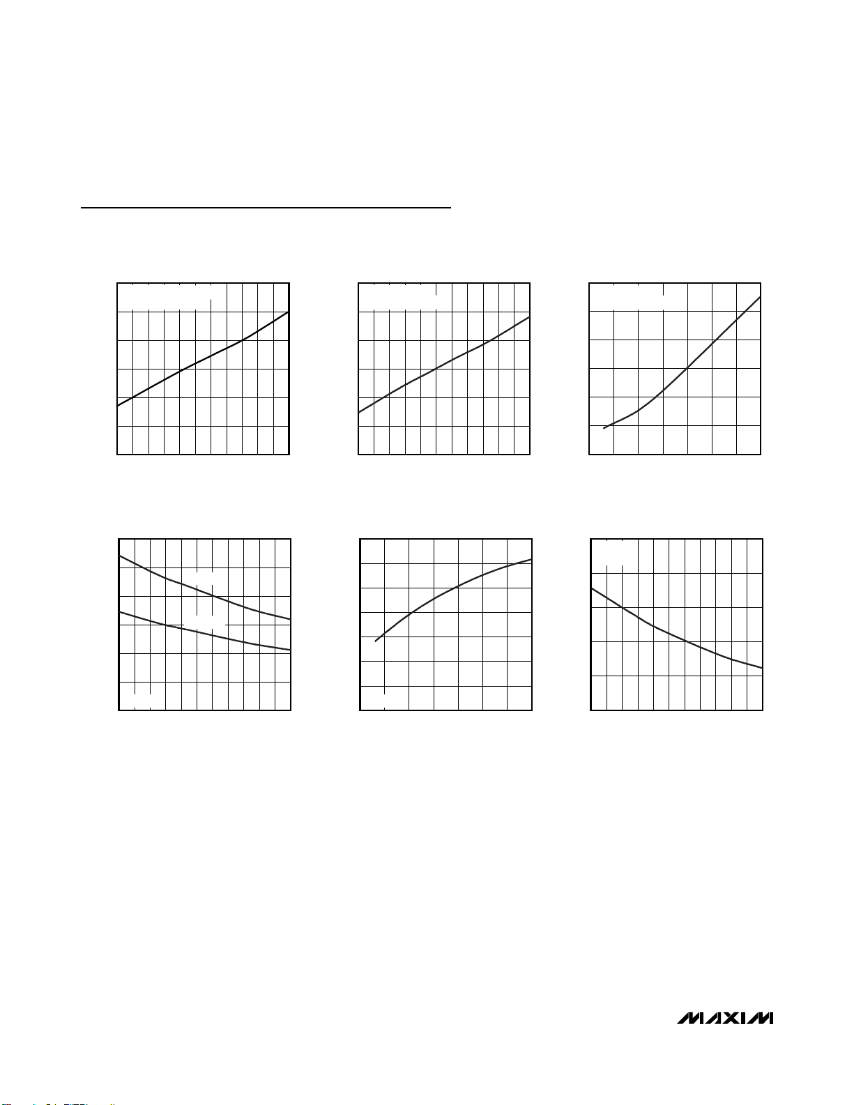
Typical Operating Characteristics
(TA = +25°C, unless otherwise noted.)
4
5
7
6
8
9
-40 -10 5 20-25 35 50 65 80 95 110 125
I/O1–I/O7 OUTPUT SOURCE CURRENT
vs. TEMPERATURE
MAX7310 toc06
TEMPERATURE (°C)
SOURCE CURRENT (mA)
V+ = 2.3V,
V
OH
= 1.4V
0
15
10
5
25
20
30
35
2.0 3.0 3.5 4.02.5 4.5 5.0 5.5
I/O0–I/O7 OUTPUT SINK CURRENT
vs. SUPPLY VOLTAGE
MAX7310 toc05
SUPPLY VOLTAGE (V)
SINK CURRENT (mA)
VOL = 0.5V
0
10
5
20
15
25
30
-40 -10 5 20-25 35 50 65 80 95 110 125
I/O0–I/O7 OUTPUT SINK CURRENT
vs. TEMPERATURE
MAX7310 toc04
TEMPERATURE (°C)
SINK CURRENT (mA)
VOL = 0.5V
VCC = 3.3V
VCC = 2.3V
10
40
20
60
70
2.0 3.0 3.5 4.02.5 4.5 5.0 5.5
SUPPLY CURRENT
vs. SUPPLY VOLTAGE
MAX7310 toc03
SUPPLY VOLTAGE (V)
SUPPLY CURRENT (µA)
30
50
f
SCL
= 440kHz,
NO LOAD ON I/O0–I/O7
1.00
1.50
1.25
2.00
1.75
2.25
2.50
-40 -10 5 20-25 35 50 65 80 95 110 125
STANDBY SUPPLY CURRENT
vs. TEMPERATURE
MAX7310 toc02
TEMPERATURE (°C)
SUPPLY CURRENT (µA)
V+ = 3.3V, f
SCL
= 0,
NO LOAD ON I/O0–I/O7
26
28
27
30
29
31
32
-40 -10 5 20-25 35 50 65 80 95 110 125
SUPPLY CURRENT
vs. TEMPERATURE
MAX7310 toc01
TEMPERATURE (°C)
SUPPLY CURRENT (µA)
V+ = 3.3V, f
SCL
= 440kHz,
NO LOAD ON I/O0–I/O7
Page 5
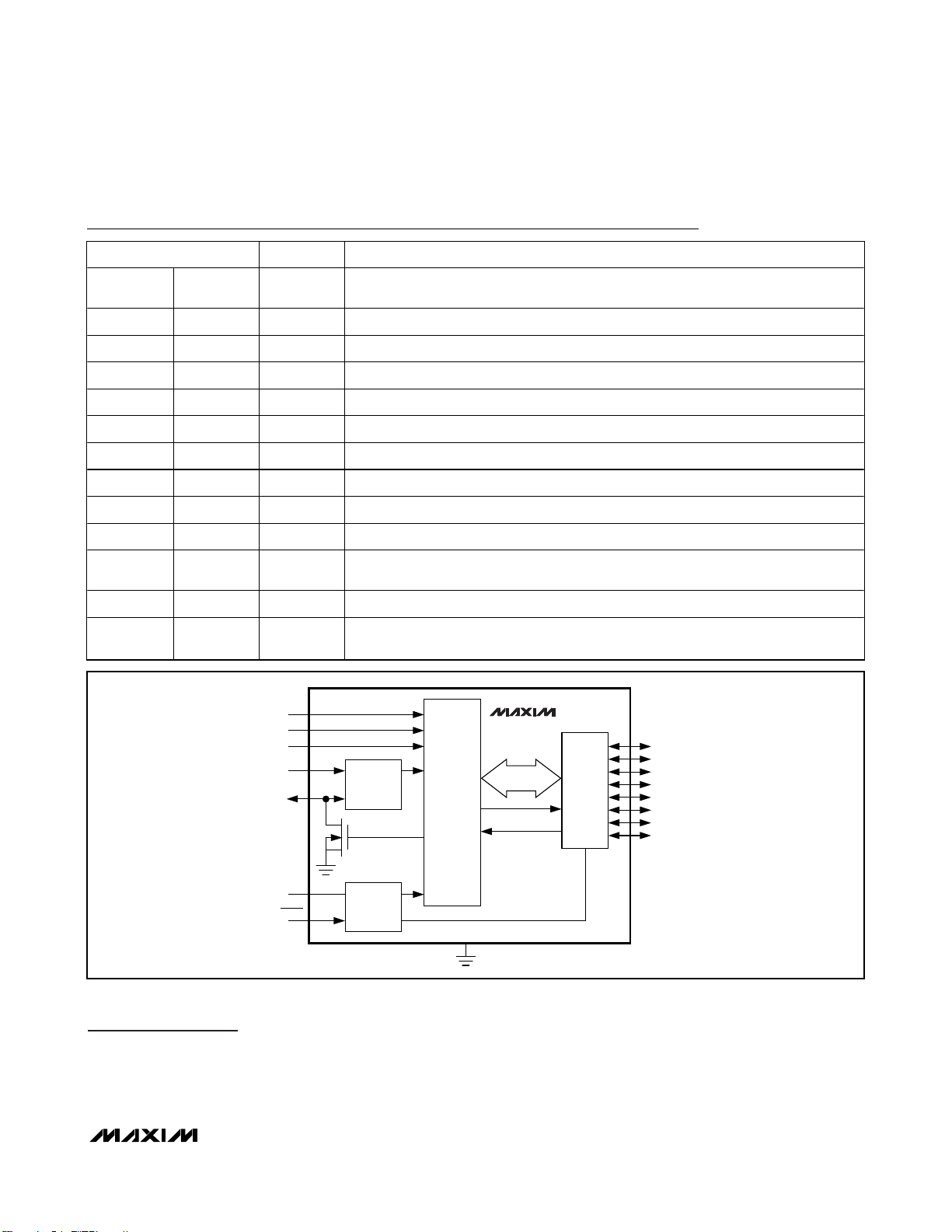
Detailed Description
The MAX7310 general-purpose input/output (GPIO)
peripheral provides up to eight I/O ports, controlled
through an I2C-compatible serial interface. The
MAX7310 consists of an input port register, an output
port register, a polarity inversion register, a configuration register, and a bus timeout register. An active-low
reset input sets the eight I/O lines as inputs. Three
slave ID address select pins (AD0, AD1, and AD2)
choose one of 56 slave ID addresses (Figure 1).
MAX7310
2-Wire-Interfaced 8-Bit I/O Port Expander
with Reset
_______________________________________________________________________________________________________ 5
Pin Description
Figure 1. MAX7310 Block Diagram
PIN
TSSOP/
QSOP
1 15 SCL Serial Clock Line
2 16 SDA Serial Data Line
3 1 AD0 Address Input 0
4 2 AD1 Address Input 1
5 3 AD2 Address Input 2
6 4 I/O0 Input/Output Port 0 (Open Drain)
7 5 I/O1 Input/Output Port 1
8 6 GND Supply Ground
9–14 7–12 I/O2–I/O7 Input/Output Port 2—Input/Output Port 7
15 13 RESET
16 14 V+ Supply Voltage. Bypass with a 0.047µF capacitor to GND.
— PAD
THIN
QFN
NAME FUNCTION
External Reset (Active Low). Pull RESET low to configure I/O pins as inputs. Set RESET
high for normal operation.
Exposed
pad
Exposed Pad on Package Underside. Connect to GND.
AD0
AD1
AD2
SCL
SDA
RESET
INPUT
FILTER
N
V+
POWER-ON
RESET
SMBus
CONTROL
WRITE PULSE
READ PULSE
GND
MAX7310
8 BIT
INPUT/
OUTPUT
PORTS
I/O0
I/O1
I/O2
I/O3
I/O4
I/O5
I/O6
I/O7
Page 6
MAX7310
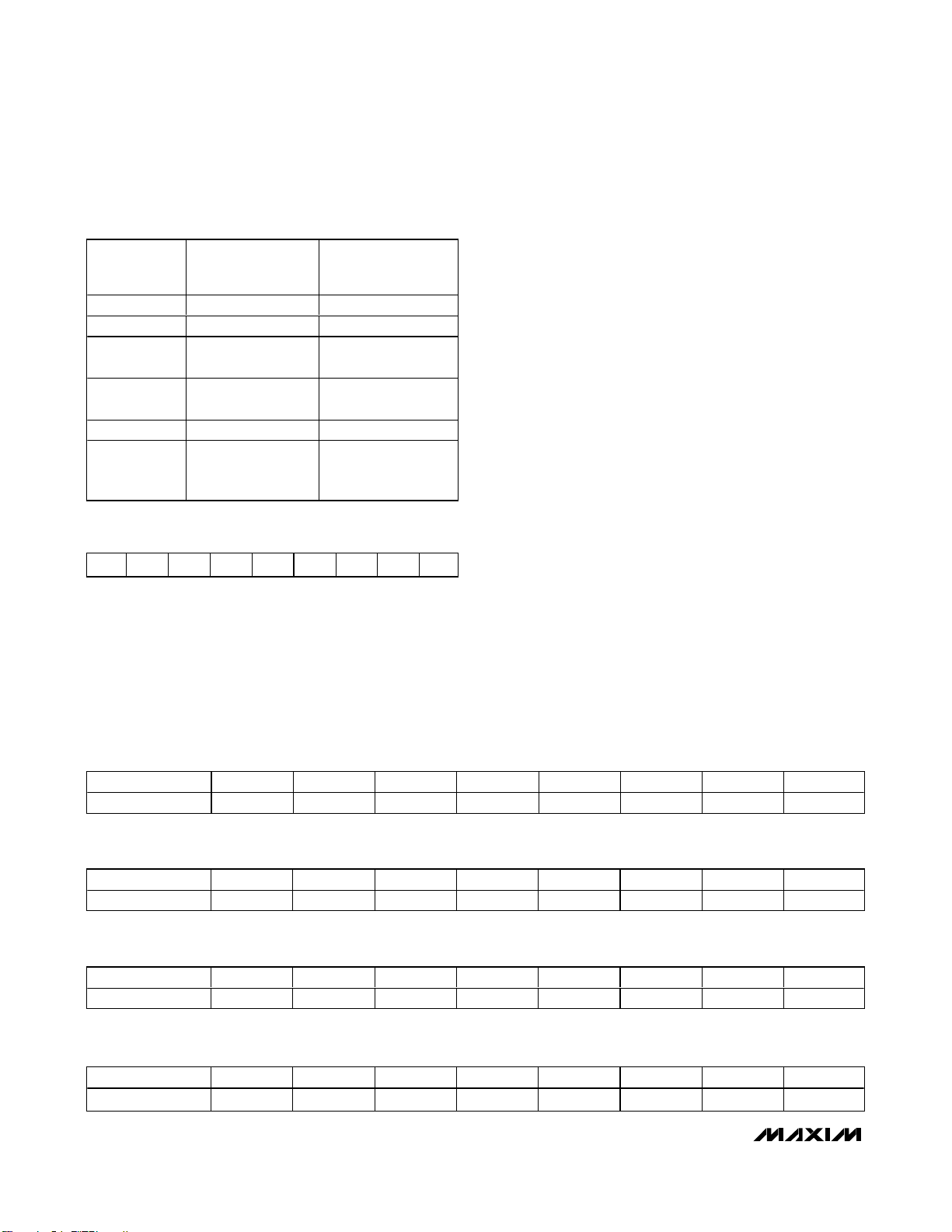
Table 1 is the register address table. Tables 2–6 list
register 0 through register 4 information.
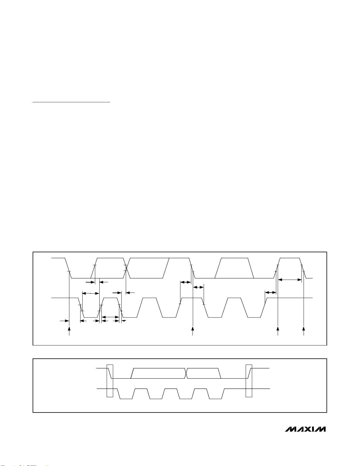
Serial Interface
Serial Addressing
The MAX7310 operates as a slave that sends and
receives data through a 2-wire interface. The interface
uses a serial data line (SDA) and a serial clock line
(SCL) to achieve bidirectional communication between
master(s) and slave(s). A master, typically a microcontroller, initiates all data transfers to and from the
MAX7310, and generates the SCL clock that synchronizes the data transfer (Figure 2).
Each transmission consists of a start condition sent by
a master, followed by the MAX7310 7-bit slave address
plus an R/W bit, a register address byte, one or more
data bytes, and finally a stop condition (Figure 3).
Start and Stop Conditions
Both SCL and SDA remain high when the interface is
not busy. A master signals the beginning of a transmission with a start (S) condition by transitioning SDA from
high to low while SCL is high. When the master has finished communicating with the slave, it issues a stop (P)
condition by transitioning SDA from low to high while
SCL is high. The bus is then free for another transmission (Figure 3).
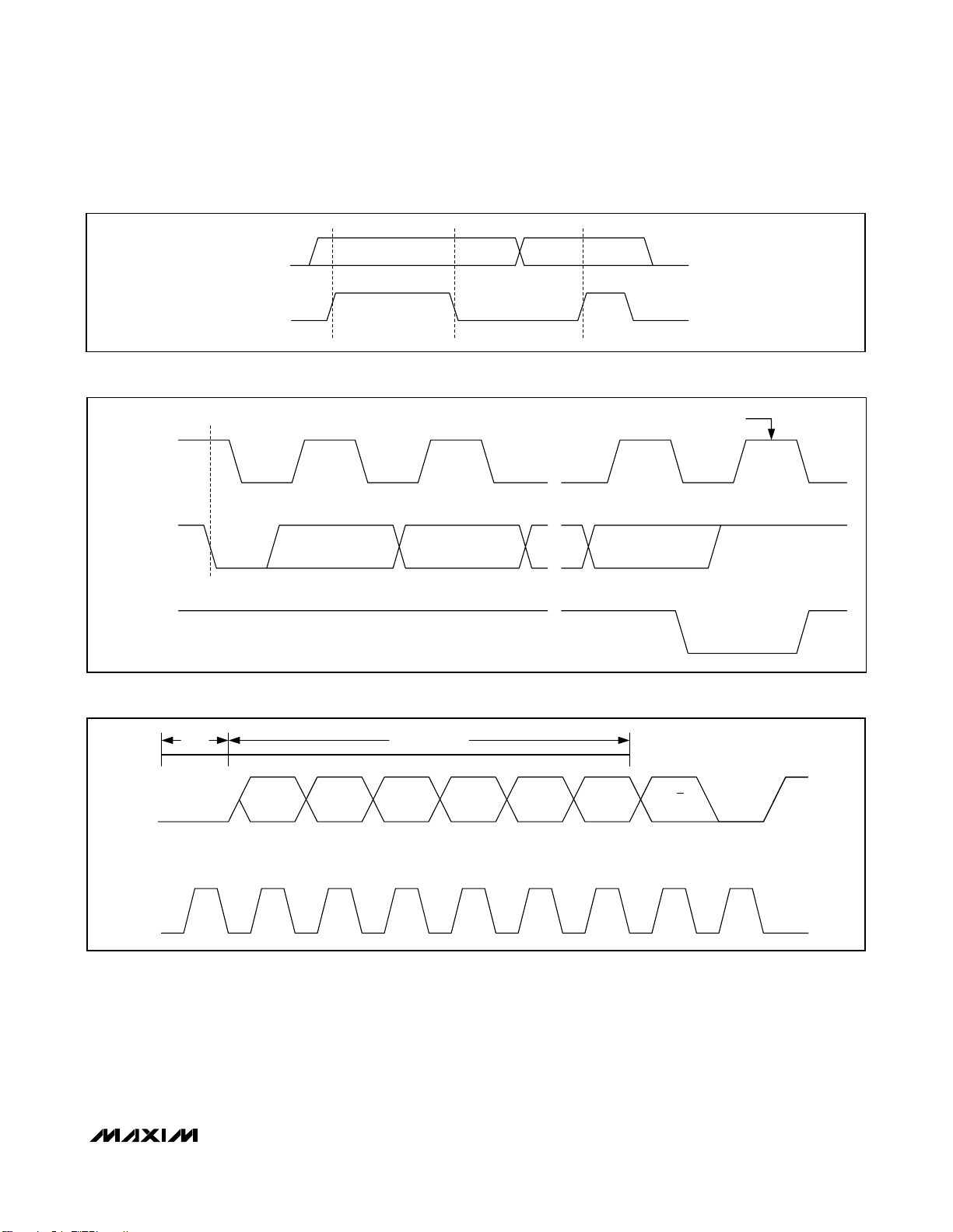
Bit Transfer
One data bit is transferred during each clock pulse.
The data on SDA must remain stable while SCL is high
(Figure 4).
Acknowledge
The acknowledge bit is a clocked 9th bit, which the
recipient uses as a handshake receipt of each byte of
data (Figure 5). Thus, each byte transferred effectively
requires 9 bits. The master generates the 9th clock
pulse, and the recipient pulls down SDA during the
acknowledge clock pulse, such that the SDA line is stable low during the high period of the clock pulse. When
the master is transmitting to the MAX7310, the
MAX7310 generates the acknowledge bit since the
MAX7310 is the recipient. When the MAX7310 is transmitting to the master, the master generates the
acknowledge bit.
Slave Address
The MAX7310 has a 7-bit-long slave address (Figure
6). The 8th bit following the 7-bit slave address is the
R/W bit. Set this bit low for a write command and high
for a read command.
2-Wire-Interfaced 8-Bit I/O Port Expander
with Reset
6 _______________________________________________________________________________________
Figure 2. 2-Wire Serial Interface Timing Diagrams
Figure 3. Start and Stop Conditions
SDA
t
SU, DAT
t
LOW
SCL
t
t
HD, STA
START CONDITION
SDA
SCL
HIGH
t
R
S
START
CONDITION
t
F
t
HD, DAT
t
SU, STA
REPEATED START CONDITION
t
HD, STA
t
P
STOP
CONDITION
SU, STO
t
BUF
START CONDITIONSTOP CONDITION
Page 7
The first bits (MSBs) of the MAX7310 slave address are
always zero. Slave address bits AD2, AD1, and AD0
choose 1 of 56 slave ID addresses (Table 7).
Registers
The register address byte is the first byte to follow the
address byte during a read/write transmission. The reg-
ister address byte acts as a pointer to determine which
register is written or read.
The input port register is a read-only port. It reflects the
incoming logic levels of the I/O ports, regardless of
whether the pin is defined as an input or an output by
the configuration register. Writes to the input port register are ignored.
MAX7310
2-Wire-Interfaced 8-Bit I/O Port Expander
with Reset
_______________________________________________________________________________________ 7
Figure 4. Bit Transfer
Figure 6. Slave Address
Figure 5. Acknowledge
SDA
SCL
DATA LINE STABLE; DATA VALID
CHANGE OF DATA ALLOWED
START CONDITION
SCL
BY TRANSMITTER
SDA
SDA
BY RECEIVER
SDA
FIXED PROGRAMMABLE
0 A2 A1 A0 ACK
CLOCK PULSE FOR ACKNOWLEDGMENT
12 89
S
A5 A4 A3
R/W
MSB LSB
SCL
Page 8
MAX7310
The output port register sets the outgoing logic levels of
the I/O ports, defined as outputs by the configuration
register. Reads from the output port register reflect the
value that is in the flip-flop controlling the output selection, not the actual I/O value, which may differ if the output is overloaded.
The polarity inversion register enables polarity inversion
of ports defined as inputs by the configuration register.
Set the bit in the polarity inversion register (write with a
1) to invert the corresponding port pin’s polarity. Clear
the bit in the polarity inversion register (write with a
zero) to retain the corresponding port pin’s original
polarity.
The configuration register configures the directions of
the ports. Set the bit in the configuration register to
enable the corresponding port pin as an input with a
high-impedance output driver. Clear the bit in the configuration register to enable the corresponding port pin
as an output.
Set bit T0 to enable the bus timeout function and low to
disable the bus timeout function. Enabling the timeout
feature resets the serial bus interface when SCL stops
either high or low during a read or write access to the
MAX7310. If either SCL or SDA is low for more than
30ms min and 60ms max after the start of a valid serial
transfer, the interface resets itself. Resetting the serial
bus interface sets up SDA as an input. The MAX7310
then waits for another start condition.
Standby
The MAX7310 goes into standby when all pins are set
to V+ or GND. Standby supply current is typically
1.7µA.
2-Wire-Interfaced 8-Bit I/O Port Expander
with Reset
8 _______________________________________________________________________________________
Table 3. Register 1—Output Port Register
Table 4. Register 2—Polarity Inversion Register
Table 5. Register 3—Configuration Register
Table 6. Register 4—Timeout Register
Table 1. Register Address
Table 2. Register 0—Input Port Register
REGISTER
ADDRESS
(hex)
0x00 Input port register Read byte.
0x01 Output port register Read/write byte.
0x02
0x03
0x04 Timeout register Read/write byte.
0xFF Reserved register
FUNCTION PROTOCOL
Polarity inversion
register
Configuration
register
Read/write byte.
Read/write byte.
Factory reserved.
Do not write to this
register.
BIT I7 I6 I5 I4 I3 I2 I1 I0
BIT O7 O6 O5 O4 O3 O2 O1 O0
Default 0 0 0 0 0 0 0 0
BIT I/O7 I/O6 I/O5 I/O4 I/O3 I/O2 I/O1 I/O0
Default 1 1 1 10000
BIT I/O7 I/O6 I/O5 I/O4 I/O3 I/O2 I/O1 I/O0
Default 1 1 1 11111
BIT T7 T6 T5 T4 T3 T2 T1 T0
Default x x x x x x x 1
Page 9

MAX7310
2-Wire-Interfaced 8-Bit I/O Port Expander
with Reset
_______________________________________________________________________________________ 9
Table 7. MAX7310 Address Map
AD2 AD1 AD0 A6 A5 A4 A3 A2 A1 A0
GNDSCLGND0001000
GNDSCLV+0001001
GNDSDAGND0001010
GNDSDAV+0001011
V+SCLGND0001100
V+SCLV+0001101
V+SDAGND0001110
V+SDAV+0001111
GNDGNDSCL0010000
GNDGNDSDA0010001
GNDV+SCL0010010
GNDV+SDA0010011
V+GNDSCL0010100
V+GNDSDA0010101
V+V+SCL0010110
V+V+SDA0010111
GND GND GND 0 0 1 1 0 0 0
GNDGNDV+0011001
GNDV+GND0011010
GNDV+V+0011011
V+GNDGND0011100
V+GNDV+0011101
V+V+GND0011110
V+V+V+0011111
SCL SCL SCL 0 1 0 0 0 0 0
SCLSCLSDA0100001
SCLSDASCL0100010
SCLSDASDA0100011
SDASCLSCL0100100
SDASCLSDA0100101
SDASDASCL0100110
SDA SDA SDA 0 1 0 0 1 1 1
SCLSCLGND0101000
SCLSCLV+0101001
SCLSDAGND0101010
SCLSDAV+0101011
SDASCLGND0101100
SDASCLV+0101101
SDASDAGND0101110
SDASDAV+0101111
Page 10

MAX7310
Applications Information
Power-Supply Consideration
The MAX7310 operates from a supply voltage of 2.3V to
5.5V. Bypass the power supply to GND with a 0.047µF
capacitor as close to the device as possible. For the
QFN version, connect the underside exposed pad to
GND.
Chip Information
TRANSISTOR COUNT: 10,256
PROCESS: BiCMOS
2-Wire-Interfaced 8-Bit I/O Port Expander
with Reset
10 ______________________________________________________________________________________
Table 7. MAX7310 Address Map (continued)
AD2 AD1 AD0 A6 A5 A4 A3 A2 A1 A0
SCLGNDSCL0110000
SCLGNDSDA0110001
SCLV+SCL0110010
SCLV+SDA0110011
SDAGNDSCL0110100
SDAGNDSDA0110101
SDAV+SCL0110110
SDAV+SDA0110111
SCLGNDGND0111000
SCLGNDV+0111001
SCLV+GND0111010
SCLV+V+0111011
SDAGNDGND0111100
SDAGNDV+0111101
SDAV+GND0111110
SDAV+V+0111111
Page 11
MAX7310
2-Wire-Interfaced 8-Bit I/O Port Expander
with Reset
______________________________________________________________________________________ 11
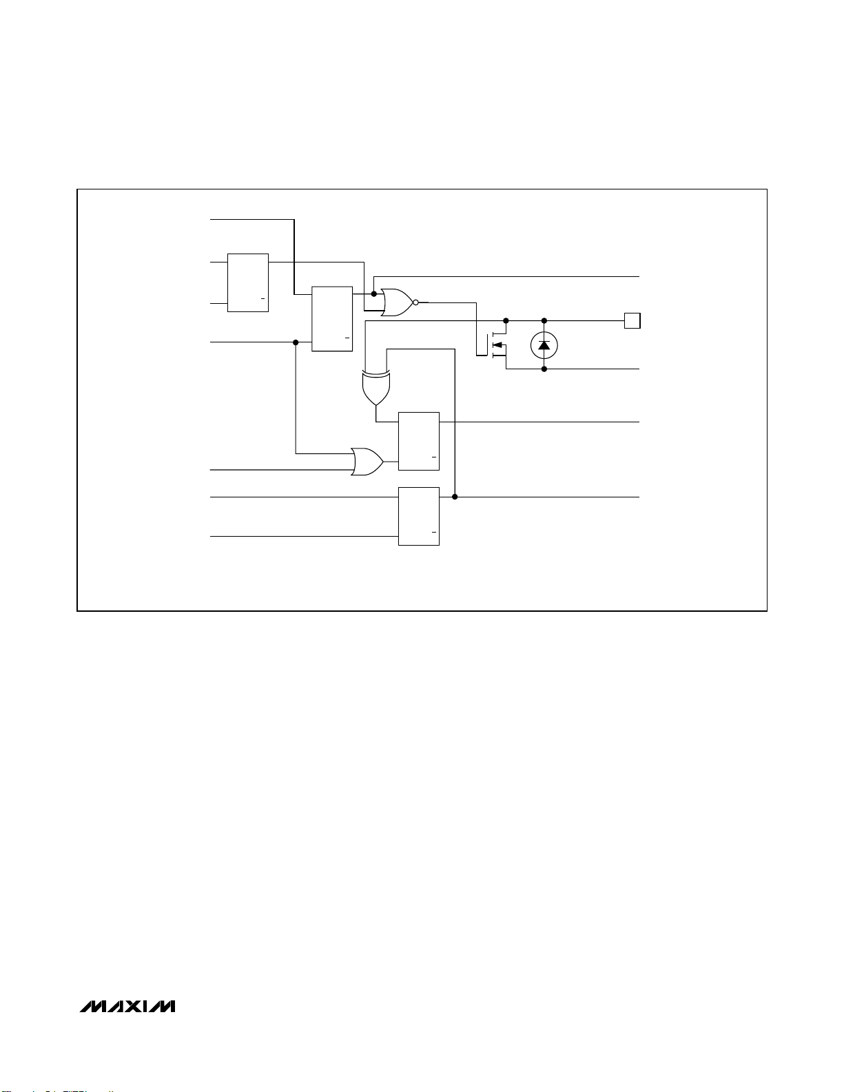
Figure 7. Simplified Schematic of I/O0
DATA FROM
SHIFT REGISTER
DATA FROM
SHIFT REGISTER
WRITE
CONFIGURATION
PULSE
WRITE PULSE
READ PULSE
CONFIGURATION
REGISTER
D
Q
FF
C
Q
K
D
FF
C
K
OUTPUT
PORT
REGISTER
OUTPUT PORT
Q
Q
INPUT
PORT
REGISTER
D
Q
FF
C
Q
K
ESD-PROTECTION DIODE
REGISTER DATA
I/O0
GND
INPUT PORT
REGISTER DATA
DATA FROM
SHIFT REGISTER
WRITE POLARITY
PULSE
D
FF
C
K
POLARITY
INVERSION
REGISTER
Q
Q
POLARITY
REGISTER DATA
Page 12

MAX7310
2-Wire-Interfaced 8-Bit I/O Port Expander
with Reset
12 ______________________________________________________________________________________
Figure 8. Simplified Schematic of I/O1–I/O7
DATA FROM
SHIFT REGISTER
DATA FROM
SHIFT REGISTER
WRITE
CONFIGURATION
PULSE
WRITE PULSE
READ PULSE
DATA FROM
SHIFT REGISTER
WRITE POLARITY
PULSE
CONFIGURATION
REGISTER
D
Q
FF
C
Q
K
D
FF
C
K
OUTPUT
PORT
REGISTER
OUTPUT PORT
REGISTER DATA
V+
ESD-PROTECTION DIODE
Q
I/O1 TO I/O7
Q
ESD-PROTECTION DIODE
INPUT
PORT
REGISTER
D
FF
C
K
D
FF
C
K
POLARITY
INVERSION
REGISTER
Q
Q
Q
Q
GND
INPUT PORT
REGISTER DATA
POLARITY
REGISTER DATA
Page 13

MAX7310
2-Wire-Interfaced 8-Bit I/O Port Expander
with Reset
______________________________________________________________________________________ 13
SCL
Figure 9. Write to Output Port Register Through Write-Byte Protocol
Figure 10. Read Input Port Register Through Receive-Byte Protocol
13245 867
9
COMMAND BYTE
0
SDA
WRITE TO
PORT
DATA OUT
FROM PORT
SLAVE ADDRESS DATA TO PORT
SAA
0A5A4A3A2A1A0 DATA 1
START CONDITION ACKNOWLEDGE
R/W
0
00
FROM SLAVE
SLAVE ADDRESS DATA FROM PORT
SDA
WRITE FROM
PORT
DATA INTO
PORT
S1 A A0 A 2 A1 A0 DATA 4
START CONDITION
A5 A4
A3
R/W
t
PH
1
ACKNOWLEDGE
FROM SLAVE
0
00
DATA FROM PORT
DATA 1
10
ACKNOWLEDGE
FROM SLAVE
ACKNOWLEDGE
FROM MASTER
t
PS
A
P
ACKNOWLEDGE
FROM SLAVE
DATA 1 VALID
t
PV
NA
P
NO ACKNOWLEDGE
FROM MASTER
DATA 4DATA 3DATA 2
STOP
CONDITION
NOTE 1: THIS FIGURE ASSUMES THE COMMAND HAS PREVIOUSLY BEEN PROGRAMMED WITH 0x00.
NOTE 2: TRANSFER OF DATA CAN BE STOPPED AT ANY MOMENT BY A STOP CONDITION. WHEN THIS OCCURS,
DATA PRESENT AT THE LAST ACKNOWLEDGED PHASE IS VALID (OUTPUT MODE). INPUT DATA IS LOST.
Page 14

MAX7310
2-Wire-Interfaced 8-Bit I/O Port Expander
with Reset
14 ______________________________________________________________________________________
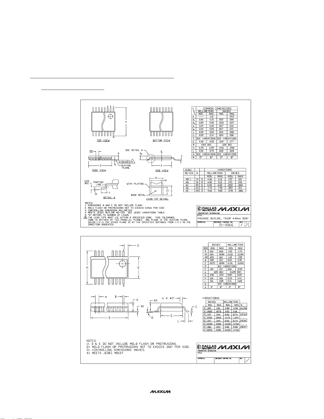
Package Information
(The package drawing(s) in this data sheet may not reflect the most current specifications. For the latest package outline information,
go to www.maxim-ic.com/packages
.)
24L QFN THIN.EPS
C
1
2
21-0139
PACKAGE OUTLINE
12, 16, 20, 24L THIN QFN, 4x4x0.8mm
C
2
2
21-0139
PACKAGE OUTLINE
12, 16, 20, 24L THIN QFN, 4x4x0.8mm
Page 15
MAX7310
2-Wire-Interfaced 8-Bit I/O Port Expander
with Reset
Maxim cannot assume responsibility for use of any circuitry other than circuitry entirely embodied in a Maxim product. No circuit patent licenses are
implied. Maxim reserves the right to change the circuitry and specifications without notice at any time.
Maxim Integrated Products, 120 San Gabriel Drive, Sunnyvale, CA 94086 408-737-7600 ____________________ 15
© 2005 Maxim Integrated Products Printed USA is a registered trademark of Maxim Integrated Products, Inc.
Package Information (continued)
(The package drawing(s) in this data sheet may not reflect the most current specifications. For the latest package outline information,
go to www.maxim-ic.com/packages
.)
TSSOP4.40mm.EPS
QSOP.EPS
PACKAGE OUTLINE, QSOP .150", .025" LEAD PITCH
21-0055
1
E
1
 Loading...