

Page 1
现货库存、技术资料、百科信息、热点资讯,精彩尽在鼎好!
For pricing, delivery, and ordering information, please contact Maxim Direct at 1-888-629-4642,
or visit Maxim's website at www.maxim-ic.com.
General Description
The MAX7302 I2C-/SMBus™-compatible, serial-interfaced
peripheral features 9 level-translating I/Os, and operates
from a 1.62V to 3.6V power supply. The MAX7302 features a port supply V
LA
that allows level-translation on I/O
ports to operate from a separate power supply from 1.62V
to 5.5V. An address select input, AD0, allows up to four
unique slave addresses for the device.
The MAX7302 ports P2–P9 can be configured as inputs,
push-pull outputs, and open-drain outputs. Port P1 can
be configured as a general-purpose input, open-drain
output, or an open-drain INT output. Ports P2–P9 can be
configured as OSCIN and OSCOUT, respectively. Ports
P2–P9 can also be used as configurable logic arrays
(CLAs) to form user-defined logic gates, replacing external discrete gates. Outputs are capable of sinking up to
25mA, and sourcing up to 10mA when configured as
push-pull outputs.
The MAX7302 includes an internal oscillator for PWM,
blink, and key debounce, or to cascade multiple
MAX7302s. The external clock can be used to set a specific PWM and blink timing. The RST input asynchronously clears the 2-wire interface and terminates a bus lockup
involving the MAX7302.
All ports configured as an output feature a 33-step PWM,
allowing any output to be set from fully off, 1/32 to 31/32
duty cycle, to fully on. All output ports also feature LED
blink control, allowing blink periods of 1/8s, 1/4s, 1/2s, 1s,
2s, 4s, or 8s. Any port can blink during this period with a
1/16 to 15/16 duty cycle.
The MAX7302 is specified over the -40°C to +125°C
temperature range and is available in 16-pin QSOP and
16-pin TQFN (3mm x 3mm) packages.
Applications
Cell Phones
Servers
System I/O Ports
LCD/Keypad Backlights
LED Status Indicators
Features
♦ 1.62V to 5.5V I/O Level-Translation Port Supply (VLA)
♦ 1.62V to 3.6V Power Supply
♦ 9 Individually Configurable GPIO Ports
P1 Open-Drain I/O
P2–P9 Push-Pull or Open-Drain I/Os
♦ Individual 33-Step PWM Intensity Control
♦ Blink Controls with 15 Steps on Outputs
♦ 1kHz PWM Period Provides Flicker-Free LED
Intensity Control
♦ 25mA (max) Port Output Sink Current (100mA
max Ground Current)
♦ Inputs Overvoltage Protected Up to 5.5V (VLA)
♦ Transition Detection with Optional Interrupt Output
♦ Optional Input Debouncing
♦ I/O Ports Configurable as Logic Gates (CLA)
♦ External RST Input
♦ Oscillator Input and Output Enable Cascading
Multiple Devices
♦ Low 0.75µA (typ) Standby Current
MAX7302
SMBus/I2C Interfaced 9-Port,
Level-Translating GPIO and LED Driver with CLA
________________________________________________________________ Maxim Integrated Products 1
Ordering Information
19-0749; Rev 0; 7/07
Pin Configurations appear at end of data sheet.
SMBus is a trademark of Intel Corp.
PART
TEMP RANGE
PINPACKAGE
PKG
CODE
MAX7302AEE+
16 QSOP
E16-4
MAX7302ATE+
16 TQFN-EP*
T1633-4
+Denotes lead-free package.
*EP = Exposed paddle.
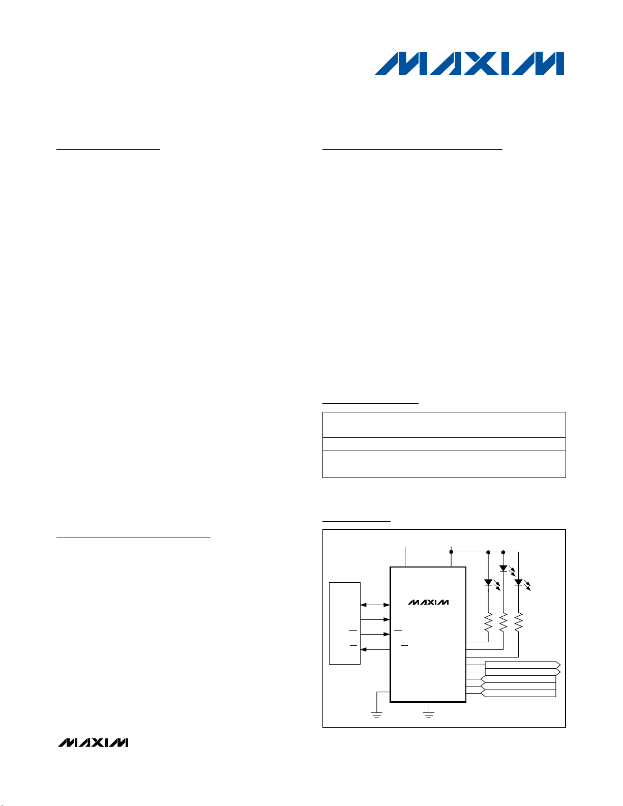
ADO
µC
SDA
GND
+1.8V
V
DD
V
LA
P2
P3
P4
P5
1.8V OPEN-DRAIN OUTPUT
P6
P7
P8
P9
+4.5V
MAX7302
4.5V PUSH-PULL OUTPUT
4.5V LOGIC INPUT
3.3V LOGIC INPUT
2.5V LOGIC INPUT
SCL
RST
INT
SDA
SCL
RST
P1/INT
Typical Operating Circuit
-40°C to +125°C
-40°C to +125°C
(3mm x 3mm)
Page 2
MAX7302
SMBus/I2C Interfaced 9-Port,
Level-Translating GPIO and LED Driver with CLA
2 _______________________________________________________________________________________
ABSOLUTE MAXIMUM RATINGS
ELECTRICAL CHARACTERISTICS
(VDD= 1.62V to 3.6V, TA= T
MIN
to T
MAX
, unless otherwise noted. Typical values are at VDD= 3.3V, VLA= 3.3V, TA= +25°C.) (Note 1)
Stresses beyond those listed under “Absolute Maximum Ratings” may cause permanent damage to the device. These are stress ratings only, and functional
operation of the device at these or any other conditions beyond those indicated in the operational sections of the specifications is not implied. Exposure to
absolute maximum rating conditions for extended periods may affect device reliability.
(All voltages referenced to GND.)
V
DD
..........................................................................-0.3V to +4V
V
LA
, SCL, SDA, AD0, RST, P1..................................-0.3V to +6V
P2–P9 ............................................................-0.3V to V
LA
+ 0.3V
P1–P9 Sink Current ............................................................25mA
P2–P9 Source Current ........................................................10mA
SDA Sink Current ...............................................................10mA
V
DD
Current .......................................................................10mA
V
LA
Current ........................................................................35mA
GND Current ....................................................................100mA
Continuous Power Dissipation (TA= +70°C)
16-Pin QSOP (derate 8.3mW/°C over +70°C)..............666mW
16-Pin TQFN (derate 14.7mW/°C over +70°C) ..........1176mW
Operating Temperature Range .........................-40°C to +125°C
Junction Temperature......................................................+150°C
Storage Temperature Range .............................-65°C to +150°C
Lead Temperature (soldering, 10s) .................................+300°C
PARAMETER
SYMBOL
CONDITIONS MIN TYP
MAX
UNITS
Operating Supply Voltage V
DD
V
Port Logic Supply Voltage V
LA
V
Power-On-Reset Voltage V
POR
VDD rising 1.0 1.3 1.6 V
Power-On-Reset Hysteresis
10 158 300
mV
I
STB
Internal oscillator disabled;
SCL, SDA, digital inputs at V
DD
or
GND; P1–P9 (as inputs) at V
LA
or
GND
0.75 2
Standby Current (Interface Idle)
I
OSC
Internal oscillator enabled;
SCL, SDA, digital inputs at V
DD
or
GND; P1–P9 (as inputs) at V
LA
or
GND
17 25
µA
S up p l y C ur r ent ( Inter face Runni ng ) I
SUP
f
SCL
= 400kHz;
31 40 µA
Port Supply Current (VLA)I
VLA
Port inputs at VLA or GND 0.06 5 µA
Input High Voltage SDA, SCL, AD0, RST V
IH
0.7 x V
DD
V
Input Low Voltage SDA, SCL, AD0, RST V
IL
V
Input High Voltage P1–P9 V
IHP
Input is VDD referred 0.7 x V
DD
V
Input Low Voltage P1–P9 V
ILP
Input is VDD referred
V
Input High Voltage P1–P9 V
IHPA
Input is VLA referred 0.7 x V
LA
V
Input Low Voltage P1–P9 V
ILPA
Input is VLA referred
V
IIH, IILVDD or GND -1 +1 µA
Input Leakage Current P1–P9
VLA or GND -2 +2 µA
Input Capacitance SDA, SCL, AD0,
P1–P9, RST
8pF
VDD = 1.62V, I
SINK
= 3mA 0.05
VDD = 2.5V, I
SINK
= 16mA 0.19
Output Low Voltage P1–P9 V
OL
VDD = 3.3V, I
SINK
= 20mA 0.19
V
VLA = 1.62V, I
SOURCE
= 0.5mA
1.58
VLA ≥ 2.5V, I
SOURCE
= 5mA
4
2.32Output High Voltage P2–P9 V
OH
VLA ≥ 3.3V, I
SOURCE
= 10mA
3.1
V
Output Low Voltage SDA
I
SINK
= 6mA 0.3 V
V
PORHYST
1.62 3.60
1.62 5.50
Inp ut Leakag e C ur r ent S D A, S C L, AD 0, RST
I
, I
IHP
ILP
V
OLSDA
other d i g i tal i np uts at VDD or G N D
0.3 x V
DD
0.3 x V
0.3 x V
DD
LA
0.11
0.31
0.31
1.55
VLA - 0.
VLA - 0.6
Page 3
MAX7302
SMBus/I2C Interfaced 9-Port,
Level-Translating GPIO and LED Driver with CLA
_______________________________________________________________________________________ 3
PORT, INTERRUPT (INT), AND RESET (RST) TIMING CHARACTERISTICS
(VDD= 1.62V to 3.6V, TA= T
MIN
to T
MAX
, unless otherwise noted. Typical values are at VDD= 3.3V, VLA= 3.3V, TA= +25°C.) (Note 1)
(Figures 10, 15, 16 and 17)
PARAMETER
CONDITIONS
TYP
UNITS
f
CLK
= internal oscillator 32 kHz
Oscillator Frequency f
CLK
1 MHz
Port Output Data Valid High Time t
PPVH
CL ≤ 100pF 4 µs
Port Output Data Valid Low Time (Note 6) t
PPVL
CL ≤ 100pF (Note 2)
s
Port Input Setup Time t
PSU
CL = 100pF 0 µs
Port Input Hold Time t
PH
CL = 100pF 4 µs
CLA Rise Time P5, P9 as Push-Pull Outputs 17
CLA Fall Time P5, P9 as Push-Pull Outputs
CL = 100pF, VLA ≥ 2.7V
14
ns
CLA Propagation Delay P2, P3, or P4 to P5; P6, P7,
or P8 to P9
CL = 100pF, VLA ≥ 2.7V 28 50 ns
INT Input Data Valid Time t
IV
CL = 100pF 4 µs
INT Reset Delay Time from Acknowledge t
IR
CL = 100pF 4 µs
RST Rising to START Condition Setup Time t
RST
ns
RST Pulse Width t
W
ns
SERIAL INTERFACE TIMING CHARACTERISTICS
(VDD= 1.62V to 3.6V, TA= T
MIN
to T
MAX
, unless otherwise noted. Typical values are at VDD= 3.3V, VLA= 3.3V, TA= +25°C.) (Note 1)
(Figure 10)
PARAMETER
CONDITIONS
TYP
UNITS
Serial-Clock Frequency f
SCL
kHz
Bus Timeout
31 ms
t
BUF
µs
Hold Time, (Repeated) START Condition
µs
Repeated START Condition Setup Time
µs
STOP Condition Setup Time
µs
Data Hold Time
(Note 3)
µs
Data Setup Time
ns
SCL Clock Low Period t
LOW
µs
SCL Clock High Period t
HIGH
µs
t
R
(Notes 2, 4)
ns
t
F
(Notes 2, 4)
ns
Fall Time of SDA Transmitting t
F.TX
(Note 4)
ns
Pulse Width of Spike Suppressed t
SP
(Note 5) 50 ns
C ap aci ti ve Load for E ach Bus Li ne C
b
(Note 2)
pF
Note 1: All parameters are tested at TA= +25°C. Specifications over temperature are guaranteed by design.
Note 2: Guaranteed by design.
Note 3: A master device must provide a hold time of at least 300ns for the SDA signal (referred to V
IL
of the SCL signal) to bridge the
undefined region of SCL’s falling edge.
Note 4: C
b
= total capacitance of one bus line in pF. tRand tFare measured between 0.3 x VDDand 0.7 x VDD.
Note 5: Input filters on the SDA and SCL inputs suppress noise spikes less than 50ns.
Note 6: A startup time is required for the internal oscilator to start if it is not running already.
SYMBOL
f
= OS C IN exter nal i np ut
C LK
t
RFCLA
t
PDCLA
Bus Fr ee Tim e Betw een a S TOP and a S TART C ond i ti on
Rise Time of Both SDA and SCL Signals, Receiving
Fall Time of Both SDA and SCL Signals, Receiving
SYMBOL
t
TIMEOUT
t
HD,STA
t
SU,STA
t
SU,STO
t
HD,DAT
t
SU,DAT
MIN
900
500
MIN
1.3
0.6
0.6
0.6
100
1.3
0.7
20 + 0.1C b 300
20 + 0.1C b 300
20 + 0.1C b 250
MAX
1 / f
CLK
MAX
400
0.9
400
Page 4
MAX7302
SMBus/I2C Interfaced 9-Port,
Level-Translating GPIO and LED Driver with CLA
4 _______________________________________________________________________________________
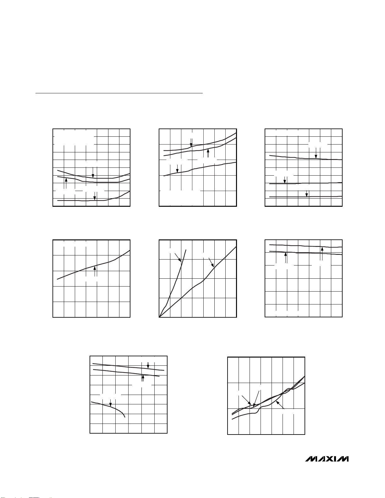
Typical Operating Characteristics
(VDD= 3.3V, VLA= 3.3V and TA= +25°C, unless otherwise noted.)
STANDBY CURRENT
vs. TEMPERATURE
MAX7302 toc01
TEMPERATURE (°C)
SUPPLY CURRENT (µA)
1007525 500-25
0.2
0.4
0.6
0.8
1.0
1.2
1.4
1.6
1.8
2.0
0
-50 125
INTERFACE IDLE
INTERNAL OSCILLATOR
DISABLED
VDD = 3.6V
VDD = 1.62V
VDD = 3.3V
STANDBY CURRENT
vs. TEMPERATURE
MAX7302 toc02
TEMPERATURE (°C)
SUPPLY CURRENT (µA)
1007525 500-25
4
8
12
16
20
0
-50 125
INTERFACE IDLE
INTERNAL OSCILLATOR
RUNNING
VDD = 3.6V
VDD = 1.62V
VDD = 3.3V
STANDBY CURRENT
vs. TEMPERATURE
MAX7302 toc03
TEMPERATURE (°C)
SUPPLY CURRENT (µA)
1007525 500-25
10
20
30
40
50
60
70
80
90
100
0
-50 125
INTERFACE RUNNING
VDD = 3.6V
VDD = 1.62V
VDD = 3.3V
VOL vs. TEMPERATURE
MAX7302 toc04
TEMPERATURE (°C)
V
OL
(V)
1007550250-25
0.06
0.12
0.18
0.24
0.30
0
-50 125
LOAD CURRENT = 20mA
VDD = 3.3V
VOL vs. I
SINK
MAX7302 toc05
I
SINK
(mA)
V
OL
(V)
30252015105
0.1
0.2
0.3
0.4
0
035
VDD = 3.3V
VDD = 1.62V
VOH vs. TEMPERATURE
MAX7302 toc06
TEMPERATURE (°C)
V
OH
(V)
1007550250-25
0.6
1.2
1.8
2.4
3.0
3.6
0
-50 125
LOAD CURRENT = 10mA
VDD = 3.6V
VDD = 3.3V
VOH vs. I
SOURCE
MAX7302 toc07
I
SOURCE
(mA)
V
OH
(V)
1082 4 6
0.5
1.0
1.5
2.0
2.5
3.0
3.5
4.0
0
012
VLA = 3.6V
VLA = 1.62V
VLA = 3.3V
INTERNAL OSCILLATOR FREQUENCY
vs. TEMPERATURE
MAX7302 toc08
TEMPERATURE (°C)
FREQUENCY (kHz)
1007550250-25
35
40
45
30
-50 125
VDD = 3.3V
VDD = 3.6V
VDD = 1.62V
Page 5
MAX7302
SMBus/I2C Interfaced 9-Port,
Level-Translating GPIO and LED Driver with CLA
_______________________________________________________________________________________ 5
Typical Operating Characteristics (continued)
(VDD= 3.3V, VLA= 3.3V and TA= +25°C, unless otherwise noted.)
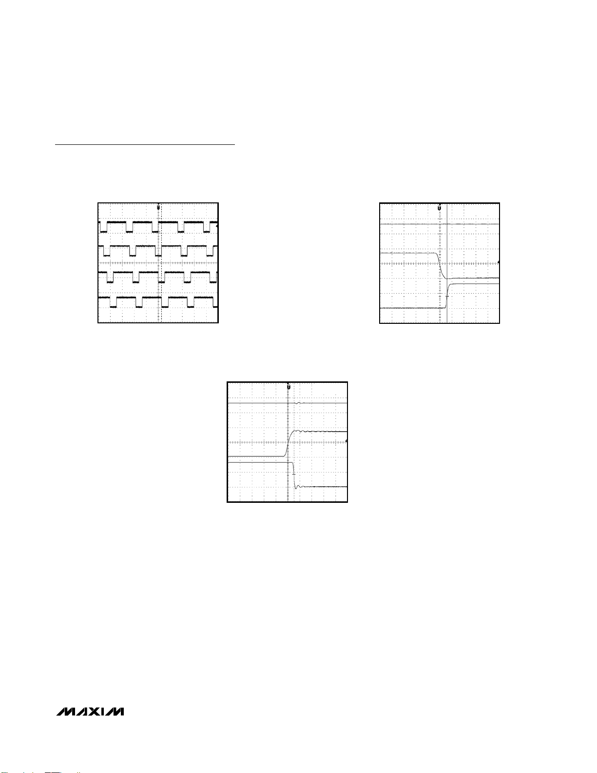
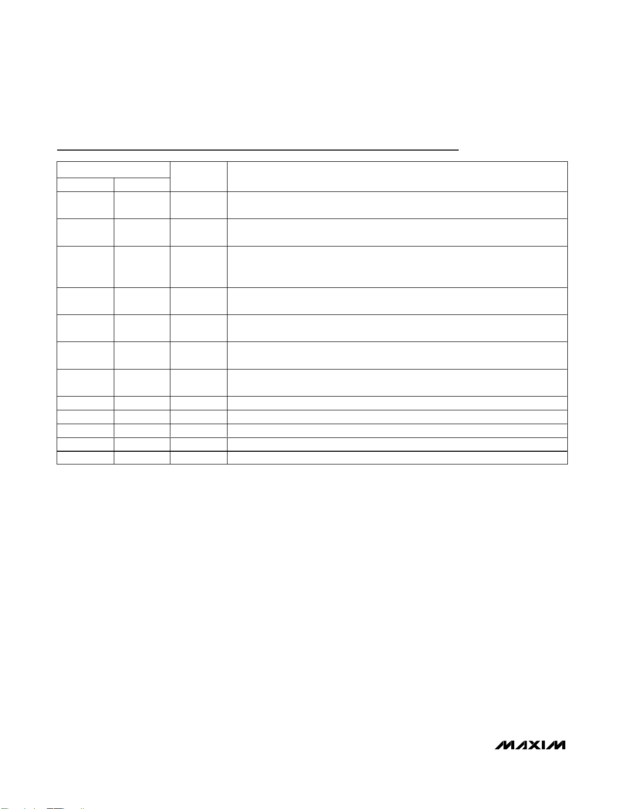
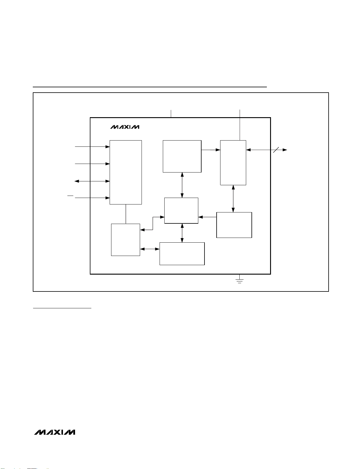
CLA PROPAGATION DELAY
OUTPUT RISING
MAX7302 toc10
40ns/div
PORT2
2V/div
PORT3
2V/div
PORT5
2V/div
CL = 100pF
MAX7302 toc11
40ns/div
CLA PROPAGATION DELAY
OUTPUT FALLING
PORT2
2V/div
PORT3
2V/div
PORT5
2V/div
CL = 100pF
PORT2
5V/div
PORT3
5V/div
PORT4
5V/div
PORT5
5V/div
STAGGERED PWM OUTPUTS
400µs/div
MAX7302 toc09
Page 6
MAX7302
SMBus/I2C Interfaced 9-Port,
Level-Translating GPIO and LED Driver with CLA
6 _______________________________________________________________________________________
Pin Description
PIN
QSOP TQFN
115V
2 16 AD0
31RST
4 2 P1/INT
5 3 P2/OSCIN
6 4 P3/OSCOUT
7, 8, 9,
11, 12, 13
10 8 GND Ground
14 12 SCL Serial-Clock Input
15 13 SDA Serial-Data I/O
16 14 V
— EP EP Exposed Paddle on Package Underside. Connect to GND.
5, 6, 7,
9, 10, 11
NAME FUNCTION
LA
P4–P9 Input/Output Ports. P4–P9 are general-purpose I/Os.
DD
Port Supply for P1–P9. Connect VLA to a power supply between 1.62V and 5.5V.
Bypass V
Address Input. Sets the device slave address. Connect to GND, V
provide four address combinations.
Reset Inp ut. RST i s an acti ve- l ow i np ut, r efer enced to V
and can b e confi g ur ed to p ut the d evi ce i n the p ow er - up r eset and /or to r eset the P W M
and b l i nk ti m i ng .
Input/Output Port. P1/INT is a general-purpose I/O that can be configured as a
transition detection interrupt output.
Input/Output Port. P2/OSCIN is a general-purpose I/O that can be configured as the
oscillator input for PWM and blink features.
Input/Output Port. P3/OSCOUT is a general-purpose I/O that can be configured as the
PWM/blink/timing oscillator output for PWM and blink features.
Positive Supply Voltage. Bypass VDD to GND with a 0.047µF ceramic capacitor.
to GND with a 0.047µF ceramic capacitor.
LA
, SCL, or SDA to
DD
, that cl ear s the 2- w i r e i nter face
DD
Page 7
MAX7302
SMBus/I2C Interfaced 9-Port,
Level-Translating GPIO and LED Driver with CLA
_______________________________________________________________________________________ 7
Detailed Description
The MAX7302 9-port, general-purpose port expander
operates from a 1.62V to 3.6V power supply. Port P1
can be configured as an input and an open-drain output. Port P1 can also be configured to function as an
INT output. Ports P2–P9 can be configured as inputs,
push-pull outputs, and open-drain outputs. Ports P2–P9
can be used as simple configurable logic arrays
(CLAs) to form user-defined logic gates.
Each port configured as an open-drain or push-pull
output can sink up to 25mA. Push-pull outputs also
have a 5mA source drive capability. The MAX7302 is
rated to sink a total of 100mA into any combination of
its output ports. Output ports have PWM and blink
capabilities, as well as logic drive.
Initial Power-Up
On power-up, the MAX7302 default configuration has all
9 ports, P1–P9, configured as input ports with logic levels referenced to VLA. The transition detection interrupt
status flag resets and stays high (see Tables 1 and 2).
Device Configuration Registers
The device configuration registers set up the interrupt
function, serial-interface bus timeout, and PWM/blink
oscillator options, global blink period, and reset options
(see Tables 3 and 4).
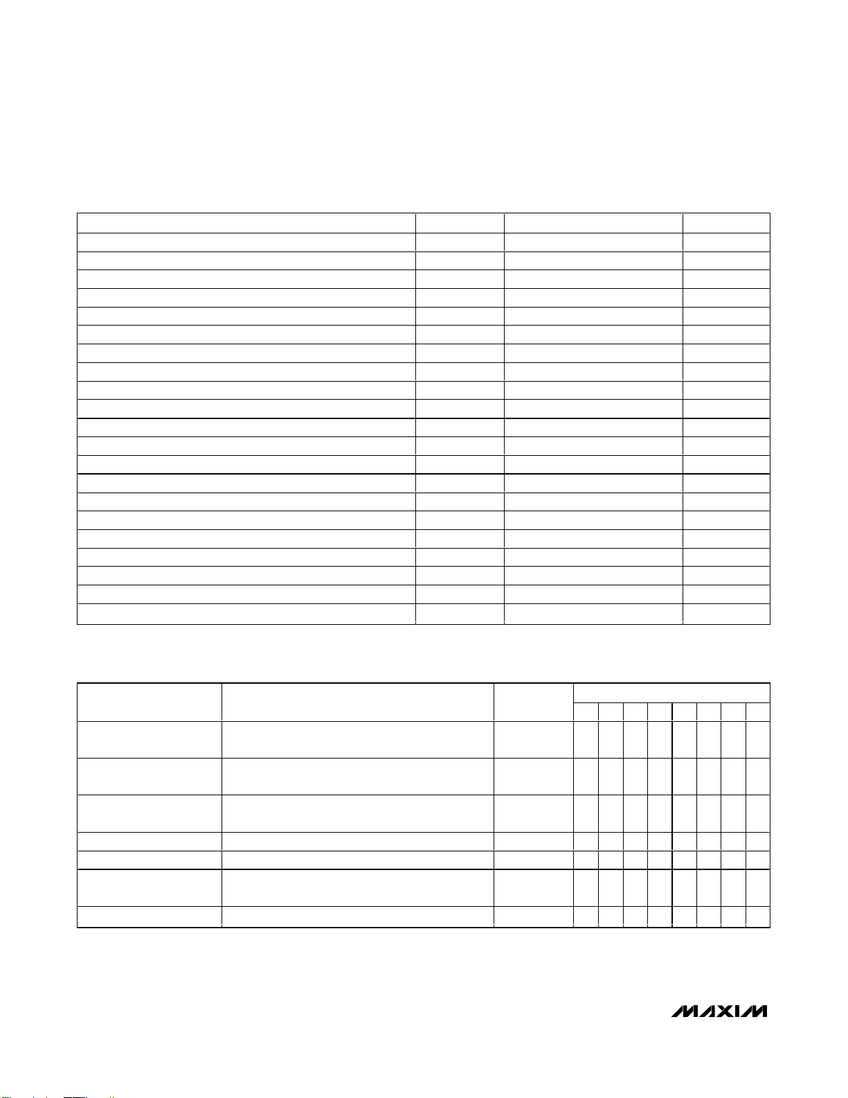
Block Diagram
AD0
SCL
SDA
RST
MAX7302
I2C
REGISTER
BANK
V
DD
OUTPUT
LOGIC
I/O
CONTROL
CLA
I/O
INPUT
LOGIC
V
LA
P1–P9
GND
Page 8
MAX7302
SMBus/I2C Interfaced 9-Port,
Level-Translating GPIO and LED Driver with CLA
8 _______________________________________________________________________________________
Table 1. Register Address Map
REGISTER DATA
REGISTER POWER-UP CONDITION
ADDRESS
D0
Ports P1–P9
Ports P_ are V
LA
-referred input ports with interrupt
and debounce disabled
0
Configuration 26
RS T d oes not r eset r eg i ster s or counters; b l i nk p er i od
i s 1H z; tr ansi ti on fl ag cl ear ; i nterr up t status fl ag cl ear
0x26
0
Configuration 27
Ports P1–P9 are GPIO ports; bus timeout is
disabled
0x27
1
Ports CLA0 to CLA1 Default gate structure
0
CLA0 to CLA1 CLA not enable 0x70
0
Configuration 27 Lock,
Ports P1–P5 Lock
Configuration 27 is not locked;
ports P1–P5 are not locked
0x72
0
Ports P6–P9 Lock Ports P6–P9 are not locked 0x73
0
Table 2. Power-Up Register Status
REGISTER ADDRESS AUTOINCREMENT ADDRESS POR STATE
Port P1 or INT Output 0x01 0x02 0x80
Port P2 or OSCIN Input 0x02 0x03 0x80
Port P3 or OSCOUT Output 0x03 0x04 0x80
Port P4 0x04 0x05 0x80
Port P5 0x05 0x06 0x80
Port P6 0x06 0x07 0x80
Port P7 0x07 0x08 0x80
Port P8 0x08 0x09 0x80
Port P9 0x09 0x0A or 0x4A 0x80
Configuration 26 0x26 0x27 0xEC
Configuration 27 0x27 0x28 0x8F
Ports P2–P5 Configurable Logic CLA0 0x28 0x29 0x00
Ports P6–P9 Configurable Logic CLA1 0x29 0x2A 0x00
Write Ports P2–P5 Same Data; Read P2 0x3C 0x3D 0x80
Write Ports P6–P9 Same Data; Read P6 0x3D 0x3E 0x80
FACTORY RESERVED (Do not write to these registers) 0x3C–0x3F 0x3F–0x40 0x00
CLA0 and CLA1 Configurable Logic Enable 0x70 0x71 0x00
CLA0 and CLA1 Configurable Logic Lock 0x71 0x72 0x00
Configuration 67 Lock, Ports P1–P5 Lock 0x72 0x73 0x00
Ports P6–P9 Lock 0x73 0x74 0xF0
FACTORY RESERVED (Do not write to these registers) 0x00 0x01 0x80
CODE (HEX)
0x01–0x09 1 0 0 0 0 0 0
0x28–0x29 0 0 0 0 0 0 0
D7 D6 D5 D4 D3 D2 D1
1110110
1000111
0000000
0000000
1111000
Page 9
MAX7302
SMBus/I2C Interfaced 9-Port,
Level-Translating GPIO and LED Driver with CLA
_______________________________________________________________________________________ 9
Table 4. Configuration Register (0x27)
REGISTER BIT
DESCRIPTION
FUNCTION
0 An interrupt has occurred on at least one interrupt enabled input port.
D7
Interrupt status flag
(read only)
1* No interrupt has occurred on an interrupt enabled input port.
0 A transition has occurred on an input port.
D6
Transition flag
(read only)
1* No transition has occurred on an input port.
D5 Reserved — Reserved
D4, D3, D2
0/1 Blink timer bits, see Table 10.
0* RST does not reset counters PWM/blink
D1 RST timer
1 RST resets PWM/blink counters
0* RST does not reset registers to power-on-reset state.
D0 RST POR
1 RST resets registers to power-on-reset state.
Table 3. Configuration Register (0x26)
*Default state.
*Default state.
VALUE
Blink prescalor bits
REGISTER BIT DESCRIPTION VALUE FUNCTION
D7 Bus timeout
D6, D5, D4 Reserved
D3 P3/OSCOUT
D2 P2/OSCIN
D1 P1/INT output
D0 Input transition 0 Set to 0 on power-up to detect transition on inputs.
0 Enables the bus timeout feature.
1 Disables the bus timeout feature.
0 Reserved
1 Reserved
0 Sets P3 to output the oscillator.
1* Sets P3 as a GPIO controlled by register 0x03.
0 Sets P2 as the oscillator input.
1* Sets P2 as a GPIO controlled by register 0x02.
0 Sets P1 as the interrupt output.
1 Sets P1 as a GPIO controlled by register 0x01.
Page 10

MAX7302
SMBus/I2C Interfaced 9-Port,
Level-Translating GPIO and LED Driver with CLA
10 ______________________________________________________________________________________
Slave Address
The MAX7302 is set to one of four I2C slave addresses,
using the address input AD0 (see Table 5) and is
accessed over an I2C or SMBus serial interface up to
400kHz. The MAX7302 slave address is determined on
each I2C transmission, regardless of whether or not the
transmission is actually addressing the device. The
MAX7302 distinguishes whether address input AD0 is
connected to SDA, SCL, VDD, or GND during the transmission. Therefore, the MAX7302 slave address can be
configured dynamically in an application without toggling the device supply.
I/O Port Registers
The port I/O registers set the I/O ports, one register per
port (see Tables 6 and 7). Ports can be independently
configured as inputs or outputs (D7), push-pull or open
drain (D6). Port P1 can only be configured as an input or
an open-drain output. The push-pull bit (D6) setting for
the port I/O register P1 is ignored.
I/O Input Port
Configure a port as an input by writing a logic-high to
the MSB (bit D7) of the port I/O register (see Table 6).
See Figure 1 for input port structure. To obtain the logic
level of the port input, read the port I/O register bit, D0.
This readback value is the instantaneous logic level at
the time of the read request if debounce is disabled for
the port (port I/O register bit D2 = 0), or the debounced
result if debounce is enabled for the port (port I/O register bit D2 = 1).
I/O Output Port
Configure a port as an output by writing a logic-low to the
MSB (bit D7) of the port I/O register. See Figures 2 and 3
for output port structure. The device reads back the logic
level, PWM, or the blink setting of the port (see Table 7).
The MAX7302 monitors the logic level of ports configured
as CLA outputs (see the Configurable Logic Array (CLA)
section).
Port Supplies and Level Translation
The port supply, VLA, provides the logic supplies to all
push-pull I/O ports. Ports P2–P9 can be configured as
push-pull I/O ports (see Figure 3). VLApowers the logic-
high port output voltage sourcing the logic-high port load
current. VLAprovides level translation capability for the
outputs and operates over a 1.62V to 5.5V voltage independent of the MAX7302 power-supply voltage, VDD.
Each port set as an input can be configured to switch
midrail of either the VDDor the VLAport supplies.
Whenever the port supply reference is changed from V
DD
to VLA, or vice versa, read the port register to clear any
transition flag on the port.
REGISTER BIT DESCRIPTION
FUNCTION
D7 Port I/O set bit 1 Sets the I/O port as an input.
0 Refers the input to the VLA supply voltage.
D6
Port supply
reference
1 Refers the input to the V
DD
supply voltage.
0 Disables the transition interrupt.
D5
Transition interrupt
enable
1 Enables the transition interrupt.
D4, D3 Reserved bits 0 Do not write to these registers.
0 Disables debouncing of the input port.
D2 Debounce
1 Enables debouncing of the input port.
0 No transition has occurred since the last port read.
D1
Port transition state
(read only)
1 A transition has occurred since the last port read.
0 Port input is logic-low.
D0
Port status
(read only)
1 Port input is logic-high.
Table 6. Port I/O Registers (I/O Port Set as an Input, Registers 0x01/0x41 to 0x09/049)
AD0
CONNECTION
A6 A5 A4 A3 A2 A1 A0
R
W
1GND
V
DD
SCL
SDA
001100
1001101
1001110
1001111
0
1
0
1
0
1
0
1
DEVICE ADDRESS
Table 5. Slave Address Selection
VALUE
Page 11

MAX7302
SMBus/I2C Interfaced 9-Port,
Level-Translating GPIO and LED Driver with CLA
______________________________________________________________________________________ 11
Figure 1. Input Port Structure
REGISTER BIT DESCRIPTION
FUNCTION
D7 Port I/O set bit 0 Sets the I/O port as an output.
0 Sets the output type to open drain.
D6
Output port set to
push-pull
or open drain
1 Sets the output type to push-pull.
0 Sets the output to PWM mode.
D5
1 Sets the output to blink mode.
D4 Duty-cycle bit 4 0/1 MSB of the 5-bit duty-cycle setting. See Tables 9 and 11.
D3 Duty-cycle bit 3 0/1 Bit 3 of the 5-bit duty-cycle setting. See Tables 9 and 11.
D2 Duty-cycle bit 2 0/1 Bit 2 of the 5-bit duty-cycle setting. See Tables 9 and 11.
D1 Duty-cycle bit 1 0/1 Bit 1 of the 5-bit duty-cycle setting. See Tables 9 and 11.
D0 Duty-cycle bit 0 0/1 LSB of the 5-bit duty-cycle setting. See Tables 9 and 11.
Table 7. Port I/O Registers (I/O Port Set as an Output, Registers 0x01 to 0x09)
V
DDVLA
PORT_ [2]
(DEBOUNCE)
PORT_ [6]
(THRESHOLD
SELECT)
PORT_ [0]
(PORTIN)
0
1
INT
TRANSITION
DETECTION
INT2
INT9
INTERRUPT
LOGIC
INT
TRANSITION
DETECTION
DEBOUNCE LOGIC
PORT_ [4:3]
PORT_ [5]
INTERRUPT
ENABLE
I/O
VALUE
PWM/blink enable
Page 12

MAX7302
SMBus/I2C Interfaced 9-Port,
Level-Translating GPIO and LED Driver with CLA
12 ______________________________________________________________________________________
Ports P2–P9 are overvoltage protected to VLA. This is true
even for a port used as an input with a V
DD
port logicinput threshold. Port P1 is overvoltage protected to 5.5V,
independent of V
DD
and VLA(see Figure 3). To mix logic
outputs with more than one voltage swing on a group of
ports using the same port supply, set the port supply voltage (V
LA
) to be the highest output voltage. Use push-pull
outputs and port P1 for the highest voltage ports, and use
open-drain outputs with external pullup resistors for the
lower voltage ports. When P2–P9 are acting as inputs referenced to V
DD
, make sure the VLAvoltage is greater
than V
DD
- 0.3V.
Port Lock Registers
Use the port lock registers to lock any combination of
port I/O register functionality (see Table 8). The port
lock registers are unlocked on power-up or by configuring the RSTPOR bit to reset to POR value. The bits in
the port lock register can only be written to once. After
setting a bit to logic-high, the bit can only be cleared
by powering off the device.
When a bit position in the port lock register is set, the
corresponding port I/O registers cannot change. When a
port I/O register is locked as an output, none of its output
register settings can change. When a port I/O register is
locked as an input, only bits D0 and D1 can change, and
the locked input behaviour options, such as debounce
and transition detection, operate as normal.
Input Debounce
The MAX7302 samples the input ports every 31ms if
input debouncing is enabled for an input port (D2 = 1
of the port I/O register). The MAX7302 compares each
new sample with the previous sample. If the new sample and the previous sample have the same value, the
corresponding internal register updates.
When the port input is read through the serial interface,
the MAX7302 does not return the instantaneous value
of the logic level from the port because debounce is
active. Instead, the MAX7302 returns the stored
debounced input signal.
Figure 3. Port I/O Structure
Figure 2. Output Port Structure
PORT_ [5]
CLOCK
SELECT
INPUT
OUTPUT
5-BIT PWM
PORT_ [4:0]
4-BIT BLINK3-BIT PRESCALER
PORT P1
PORT_ [3:0]
SELECT
INPUT
OUTPUT
CONFIG26 [4:2]
V+ V
LA
P1 P2–P9
0
1
V+ V
I/O
LA
PORT
P2–P9
Page 13

MAX7302
SMBus/I2C Interfaced 9-Port,
Level-Translating GPIO and LED Driver with CLA
______________________________________________________________________________________ 13
When debouncing is enabled for a port input, transition
detection applies to the stored debounced input signal
value, rather than to the instantaneous value at the
input. This process allows for useful transition detection
of noisy signals, such as keyswitch inputs, without
causing spurious interrupts.
Port Input Transition Detection and Interrupt
Any transition on ports configured as inputs automatically
set the D1 bit of that port’s I/O registers high. Any input can
be selected to assert an interrupt output indicating a transition has occurred at the input port(s). The MAX7302 samples the port input (internally latched into a snapshot
register) during a read access to its port P_ I/O register.
The MAX7302 continuously compares the snapshot with
the port’s input condition. If the device detects a change
for any port input, an internal transition flag sets for that
port. Read register 0x26 to clear the interrupt, then read all
the port I/O registers (0x01 to 0x09) by initiating a burst
read to clear the MAX7302’s internal transition flag. Note
that when debouncing is enabled for a port input, transition
detection applies to the stored debounced input signal
value, rather than to the instantaneous value at the input.
Transition bits D4 and D3 must be set to 0 to detect the
next rising or falling edge on the input port P_.
The MAX7302 allows the user to select the input port(s)
that cause an interrupt on the INT output. Set INT for
each port by using the INTenable bit (bit D5) in each
port P_ register. The appropriate port’s transition flag
always sets when an input changes, regardless of the
port’s INTenable bit settings. The INTenable bits allow
processor interrupt only on critical events, while the
inputs and the transition flags can be polled periodically to detect less critical events.
When debounce is disabled, signal transtions between
the 9th and 11th falling edges of clock will not be registered since the transition is detected and cleared at the
same read cycle.
Ports configured as outputs do not feature transition
detection, and therefore, cannot cause an interrupt.
The exception to this rule is the CLA outputs.
The INT output never reasserts during a read sequence
because this process could cause a recursive reentry
into the interrupt service routine. Instead, if a data
change occurs during the read that would normally set
the INT output, the interrupt assertion is delayed until
the STOP condition. If the changed input data is read
before the STOP condition, a new interrupt is not
required and not asserted. The INT bit and INT output
(if selected) have the same value at all times.
Transition Flag
The Transition bit in device configuration register 0x26 is
a NOR of all the port I/O registers’ individual Transition
bits. A port I/O register’s Transition bit sets when that
port is set as an input, and the input changes from the
port’s I/O registers last read through the serial interface.
A port’s individual Transition bit clears by reading that
port’s I/O register. The Transition flag of configuration
register 0x26 is only cleared after reading all port I/O
registers on which a transition has occurred.
RST
Input
The active-low RST input operates as a hardware reset
which voids any on-going I
2
C transaction involving the
MAX7302. This feature allows the MAX7302 supply current to be minimized in power critical applications by
effectively disconnecting the MAX7302 from the bus.
RST also operates as a chip enable, allowing multiple
devices to use the same I2C slave address if only one
MAX7302 has its RST input high at any time. RST can
be configured to restore all port registers to the powerup settings by setting bit D0 of device configuration register 0x26 (Table 1). RST can also be configured to reset
the internal timing counters used for PWM and blink by
setting bit D1 of device configuration register 0x26.
When RST is low, the MAX7302 is forced into the I2C
STOP condition. The reset action does not clear the
interrupt output INT. The RST input is referenced to V
DD
and is overvoltage tolerant up to the supply voltage, VLA.
REGISTER DATA
ADDRESS
CODE
D7 D6 D5 D4 D3 D2 D1 D0
0x72
Port
P5
Port
P4
Port
P3
Port
P2
Port
P1
—
Configuration
0
0x73 — — — —
Port
P9
Port
P8
Port
P7
Port
P6
Table 8. Port Lock Registers
register 0x27
Page 14

MAX7302
SMBus/I2C Interfaced 9-Port,
Level-Translating GPIO and LED Driver with CLA
14 ______________________________________________________________________________________
INT
Output
Port P1 can be configured as a latching interrupt output, INT, that flags any transients on any combination of
selected ports configured as inputs. Configurable logic
gate outputs can also be monitored as readback inputs
with the same options as normal I/O port inputs. Any
transitions occurring at the selected inputs assert INT
low to alert the host processor of data changes at the
selected inputs. Reset INT by reading any ports I/O
registers (0x01 to 0x09).
Standby Mode
Upon power-up, the MAX7302 enters standby mode
when the serial interface is idle. If any of the PWM
intensity control, blink, or debounce features are used,
the operating current rises because the internal PWM
oscillator is running and toggling counters. When using
OSCIN to override the internal oscillator, the operating
current varies according to the frequency at OSCIN.
When the serial interface is active, the operating current also increases because the MAX7302, like all I
2
C
slaves, has to monitor every transmission. The bus
timeout and debounce circuits use the internal oscillator even if OSCIN is selected.
Internal Oscillator and OSCIN/OSCOUT
External Clock Options
The MAX7302 contains an internal 32kHz oscillator. The
MAX7302 always uses the internal oscillator for bus
timeout and for debounce timing (when enabled). It is
used by default to generate PWM and blink timing. The
internal oscillator only runs when the clock output
OSCOUT is needed to keep the operating current as
low as possible.
The MAX7302 can use an external clock source instead
of the internal oscillator for the PWM and blink timing.
The external clock can range from DC to 1MHz, and it
connects to the P2/OSCIN port. The P3/OSCOUT port
provides a buffered and level-shifted output of the internal oscillator or external clock to drive other devices.
Select the P2/OSCIN and P3/OSCOUT port options
using the device configuration register 0x67 bits D2
and D3 (see Table 4).
The P2/OSCIN port is overvoltage protected to supply
voltage V
LA
, so the external clock can exceed VDDif
V
LA
is greater than VDD. The port P2 register (see
Tables 2 and 6) sets the P2/OSCIN logic threshold
(30%/70%) to either the V
DD
supply or the VLA.
Use OSCOUT or an external clock source to cascade
up to four MAX7302s per master for applications requiring additional ports. To synchronize the blink action
across multiple MAX7302s (see Figures 4 and 5), use
OSCOUT from one MAX7302 to drive OSCIN of the
other MAX7302s. This process ensures the same blink
frequency of all the devices, but also make sure to synchronize the blink phase. The blink timing of multiple
MAX7302s is synchronous at the instant of power-up
because the blink and PWM counters clear by each
MAX7302’s internal reset circuit, and by default the
MAX7302s’ internal oscillators are off upon power-up.
Ensure that the blink phase of all the devices remains
synchronized by programming the OSCIN and
OSCOUT functionality before programming any feature
that causes a MAX7302’s internal oscillator to operate
(blink, PWM, bus timeout, or key debounce). Configure
the RST input to reset the internal timing counters used
for PWM and blink by setting bit D1 of device configuration register 0x26 (see Table 3).
PWM and Blink Timing
The MAX7302 divides the 32kHz nominal internal oscillator OSC or external clock source OSCIN frequency by 32
to provide a nominal 1kHz PWM frequency. Use the reset
Figure 4. Synchronizing Multiple MAX7302s (Internal Oscillator)
MAX7302
P3/OSCOUT
MAX7302
P3/OSCOUT
MAX7302
P2/OSCIN
MAX7302
P2/OSCIN P3/OSCOUT
MAX7302
P2/OSCIN
MAX7302
P2/OSCIN
Page 15

MAX7302
SMBus/I2C Interfaced 9-Port,
Level-Translating GPIO and LED Driver with CLA
______________________________________________________________________________________ 15
function to synchronize multiple MAX7302s that are operating from the same OSCIN, or to synchronize a single
MAX7302’s blink timing to an external event. Configure
the RST input to reset the internal timing counters used by
PWM and blink by setting bit D1 of the device configuration register 0x26 (see Table 3).
The MAX7302 uses the internal oscillator by default.
Configure port P2 using device configuration register
0x27 bit D2 (see Table 4) as an external clock source
input, OSCIN, if the application requires a particular or
more accurate timing for the PWM or blink functions.
OSCIN only applies to PWM and blink; the MAX7302
always uses the internal oscillator for debouncing and
bus timeout. OSCIN can range up to 1MHz. Use device
configuration register 0x27 bit D3 (see Table 4) to configure port P3 as OSCOUT to output a MAX7302’s
clock. The MAX7302 buffers the clock output of either
the internal oscillator OSC or the external clock source
OSCIN, according to port D2’s setup. Synchronize multiple MAX7302s without using an external clock source
input by configuring one MAX7302 to generate
OSCOUT from its internal clock, and use this signal to
drive the remaining MAX7302s’ OSCIN.
A PWM period contains 32 cycles of the nominal 1kHz
PWM clock (see Figure 6). Set ports individually to a
PWM duty cycle between 0/32 and 31/32. For static
logic-level low output, set the ports to 0/32 PWM, and
for static logic-level high output, set the port register to
0111XXXX (see Table 9). The MAX7302 staggers the
PWM timing of the 9-port outputs, in single or dual
ports, by 1/8 of the PWM period. These phase shifts
distribute the port-output switching points across the
PWM period (see Figure 7). This staggering reduces
the di/dt output-switching transient on the supply and
also reduces the peak/mean current requirement.
All ports feature LED blink control. A global blink period
of 1/8s, 1/4s, 1/2s, 1s, 2s, 4s, or 8s applies to all ports
(see Table 10). Any port can blink during this period
with a 1/16 to 15/16 duty cycle, adjustable in 1/16
increments (see Table 11). For PWM fan control, the
MAX7302 can set the blink frequency to 32Hz.
Figure 5. Synchronizing Multiple MAX7302s (External Clock)
REGISTER DATA
PWM SETTINGS
D7 D6 D5 D4 D3 D2 D1 D0
Port P_ is a static logic-level low output port 0 X 0 0 0 0 0 0
Port P_ is a PWM output port; PWM duty cycle is 1/32 0 X 0 0 0 0 0 1
Port P_ is a PWM output port; PWM duty cycle is 2/32 0 X 0 0 0 0 1 0
Port P_ is a PWM output port; PWM duty cycle is 3/32 0 X 0 0 0 0 1 1
Port P_ is a PWM output port; PWM duty cycle is 4/32 0 X 0 0 0 1 0 0
……
Port P_ is a PWM output port; PWM duty cycle is 30/32 0 X 0 1 1 1 1 0
Port P_ is a PWM output port; PWM duty cycle is 31/32 0 X 0 1 1 1 1 1
Port P_ is a static logic-level high output port 0 1 1 1 X X X X
Table 9. PWM Settings on Output Port
EXTERNAL
OSCILLATOR
EXTERNAL
OSCILLATOR
0 TO 1MHz
0 TO 1MHz
P2/OSCIN
P2/OSCIN
MAX7302
MAX7302
P3/OSCOUT
P2/OSCIN P2/OSCIN
P2/OSCIN P3/OSCOUT P2/OSCIN
MAX7302
MAX7302
MAX7302
MAX7302
Page 16

MAX7302
SMBus/I2C Interfaced 9-Port,
Level-Translating GPIO and LED Driver with CLA
16 ______________________________________________________________________________________
Figure 6. Static and PWM Port Output Waveforms
Figure 7. Staggered PWM Phasing Between Port Outputs
PORT
REGISTER
VALUE
0b0X000000
0b0X000001
0b0X000010
0b0X000011
OUTPUT STATIC LOW (STATIC LOGIC-LOW OUTPUT OR LED DRIVE ON)
OUTPUT LOW 1/32 DUTY PWM
OUTPUT LOW 2/32 DUTY PWM
OUTPUT LOW 3/32 DUTY PWM
977µs NOMINAL PWM PERIOD (1024Hz PERIOD)
HIGH-Z
LOW
HIGH-Z
LOW
HIGH-Z
LOW
HIGH-Z
LOW
0b0X011101
0b0X011110
0b0X011111
0b0111XXXX
OUTPUT LOW 29/32 DUTY PWM
OUTPUT LOW 30/32 DUTY PWM
OUTPUT LOW 31/32 DUTY PWM
OUTPUT STATIC HIGH (STATIC LOGIC-HIGH OUTPUT OR LED DRIVE OFF)
977µs NOMINAL PWM PERIOD
012
345678
OUTPUT P8
OUTPUTS P1, P9 OUTPUTS P1, P9 OUTPUTS P1, P9
OUTPUT P2 OUTPUT P2 OUTPUT P2
OUTPUT P3 OUTPUTP3 OUTPUT P3
HIGH-Z
LOW
HIGH-Z
LOW
HIGH-Z
LOW
HIGH-Z
LOW
NEXT PWM PERIOD NEXT PWM PERIOD
OUTPUT P8 OUTPUT P8
OUTPUT P4 OUTPUT P4
OUTPUT P5 OUTPUT P5
OUTPUT P6 OUTPUT P6
OUTPUT P7 OUTPUT P7
Page 17

MAX7302
SMBus/I2C Interfaced 9-Port,
Level-Translating GPIO and LED Driver with CLA
______________________________________________________________________________________ 17
Table 11. Blink Settings on Output Ports
REGISTER BIT
FUNCTION
D5 D4 D3 D2 D1 D0
XOR noninverted 00
XOR P3 inverted 10
XOR P2 inverted 01
XOR both ports inverted
01X
1
X
1
3 input AND/OR all noninverted 0 0 0
3 input AND/OR P2 inverted 0 0 1
3 input AND/OR P3 inverted 0 1 0
3 input AND/OR P4 inverted 0 1 1
3 input AND/OR P2 and P3 inverted 1 0 0
3 input AND/OR P2 and P4 inverted 1 0 1
3 input AND/OR P3 and P4 inverted 1 1 0
3 input AND/OR all inverted
1
1
1
1
1
1
Table 12. CLA0 (P2–P5) Configuration Register Setting (0x28)
DEVICE CONFIGURATION
REGISTER 0x26
BLINK OR PWM SETTING
BLINK OR PWM
FREQUENCY (32kHz
INTERNAL OSCILLATOR)
(Hz)
BLINK OR PWM
FREQUENCY (0 TO 1MHz
EXTERNAL OSCILLATOR)
Bl i nk p er i od i s 8s ( 0.125H z) 0 0 0 0.125 OSCIN / 262,144
Blink period is 4s (0.25Hz) 0 0 1 0.25 OSCIN / 131,072
Blink period is 2s (0.5Hz) 0 1 0 0.5 OSCIN / 65,536
Blink period is 1s (1Hz) 0 1 1 1 OSCIN / 32,768
Blink period is a 1/2s (2Hz) 1 0 0 2 OSCIN / 16,384
Blink period is a 1/4s (4Hz) 1 0 1 4 OSCIN / 8192
Bl i nk p er i od i s an 1/8s ( 8H z) 1 1 0 8 OSCIN / 4096
Bl i nk p er i od i s a 1/32s ( 32H z) 1 1 1 32 OSCIN / 1024
PWM X X X 1024 OSCIN / 32
Table 10. Blink and PWM Frequencies
BIT D4
BLINK2
BIT D3
BLINK1
BIT D2
BLINK0
PWM SETTINGS
Port P_ is a static logic-level low output port 0 X 1 00000
Port P_ is a PWM output port; PWM duty cycle is 1/16 0 X 1 00001
Port P_ is a PWM output port; PWM duty cycle is 2/16 0 X 1 00010
Port P_ is a PWM output port; PWM duty cycle is 3/16 0 X 1 00100
……
Port P_ is a PWM output port; PWM duty cycle is 14/16 0 X 1 0 1 1 1 0
Port P_ is a PWM output port; PWM duty cycle is 15/16 0 X 1 0 1 1 1 1
Port P_ is a static logic-level high output port (32/32) 0 1 1 1 X X X X
D7 D6 D5 D4 D3 D2 D1 D0
REGISTER DATA
Page 18

MAX7302
SMBus/I2C Interfaced 9-Port,
Level-Translating GPIO and LED Driver with CLA
18 ______________________________________________________________________________________
Table 13. Output P5 Configuration
REGISTER BIT
FUNCTION
D5 D4 D3 D2 D1 D0
2 input AND/OR P2 and P3 noninverted 0 0
2 input AND/OR P2 and P3 inverted 1 0
2 input AND/OR P2 inverted and P3 0 1
2 input AND/OR P2 and P3 both inverted
0X1
1
1
1
2 input AND/OR P2 and P4 noninverted 0 0
2 input AND/OR P2 and P4 inverted 1 0
2 input AND/OR P2 inverted and P4 0 1
2 input AND/OR P2 and P4 both inverted
1
1
0X1
1
2 input AND/OR P3 and P4 noninverted 0 0
2 input AND/OR P3 and P4 inverted 0 1
2 input AND/OR P3 inverted and P4 1 0
2 input AND/OR P3 and P4 both inverted
1
1
1
1
0X
Table 12. CLA0 (P2–P5) Configuration Register Setting (0x28) (continued)
REGISTER BIT
FUNCTION
D5 D4 D3 D2 D1 D0
XOR noninverted 00
XOR P7 inverted 10
XOR P6 inverted 01
XOR both ports inverted
01X
1
X
1
3 input AND/OR all noninverted 0 0 0
3 input AND/OR P6 inverted 0 0 1
3 input AND/OR P7 inverted 0 1 0
3 input AND/OR P8 inverted 0 1 1
3 input AND/OR P6 and P7 inverted 1 0 0
3 input AND/OR P6 and P8 inverted 1 0 1
3 input AND/OR P7 and P8 inverted 1 1 0
3 input AND/OR all inverted
1
1
1
1
1
1
2 input AND/OR P6 and P7 noninverted 0 0
2 input AND/OR P6 and P7 inverted 1 0
2 input AND/OR P6 inverted and P7 0 1
2 input AND/OR P6 and P7 both inverted
0X1
1
1
1
Table 14. CLA1 (P6–P9) Configuration Register Setting (0x29)
BIT LOGIC LEVEL FUNCTION
D7
D6
0 Output not cascaded to CLA1
1 Output cascaded to CLA1
0 Output noninverted
1 Output inverted
Page 19

MAX7302
SMBus/I2C Interfaced 9-Port,
Level-Translating GPIO and LED Driver with CLA
______________________________________________________________________________________ 19
Table 16. Configurable Logic-Array
Enable Register (0x70)
BIT
FUNCTION
0 Cascade input noninverted
D7
1 Cascade input inverted
0 Output noninverted
D6
1 Output inverted
Table 15. Output P9 and Cascade P5
Input Configuration
REGISTER BIT
FUNCTION
D5 D4 D3 D2 D1 D0
2 input AND/OR P6 and P8 noninverted 0 0
2 input AND/OR P6 and P8 inverted 1 0
2 input AND/OR P6 inverted and P8 0 1
2 input AND/OR P6 and P8 both inverted
1
1
0X1
1
2 input AND/OR P7 and P8 noninverted 0 0
2 input AND/OR P7 and P8 inverted 0 1
2 input AND/OR P7 inverted and P8 1 0
2 input AND/OR P7 and P8 both inverted
1
1
1
1
0X
Table 14. CLA1 (P6–P9) Configuration Register Setting (0x29)(continued)
REGISTER DATA
REGISTER
D1 D0
CLA0 and CLA1 configurable
logic lock
CLA0
CLA0 is not locked — X 0
CLA0 is locked — X 1
CLA1 is not locked — 0 X
CLA1 is locked — 1 X
Table 17. Configurable Logic-Array Lock
Register (0x71)
LOGIC LEVEL
D7–D2
CLA1
REGISTER
CLA0 and CLA1 configurable
logic enable
Ports P2–P5 are GPIO ports — X 0
Ports P2–P5 are configurable logic
CLA0
Ports P6–P9 are GPIO ports — 0 X
Ports P6–P9 are configurable logic
CLA1
REGISTER DATA
D7–D2 D1 D0
CLA1 CLA0
—X 1
—1 X
Page 20

MAX7302
SMBus/I2C Interfaced 9-Port,
Level-Translating GPIO and LED Driver with CLA
20 ______________________________________________________________________________________
Table 18. Port I/O Registers (I/O Port 5 and 9 Configured as CLA Outputs, Registers
0x05 and 0x09)
Configurable Logic Array (CLA)
The CLA configures groups of four ports as either a
combinational logic gate up to three inputs, or a two
input exclusive OR/NOR gate (see Tables 12-15).
Eight-port dual groups can be cascaded to form a
two-level gate with the intermediate term brought out
as an output or not, as desired. If fewer than three
gate inputs are needed, the unused CLA input(s)
(which can be any combination of the three CLA
inputs) remain available as independent GPIO ports
(see Figure 8). Use the configurable logic-array enable
register (see Table 16) to enable ports as CLAs. Use the
configurable logic-array lock register (see Table 17) to
permanently lock in any logic-array combination of CLAs
until the next power cycle. Setting D0 and D1 to logichigh in the configurable logic-array lock register locks the
corresponding bit position in the configurable logic-array
enable register. Additionally, the appropriate CLA_ register (addresses 0x28 and 0x29) cannot be changed.
The configurable logic-array lock register is unlocked
on power-up, or by RST when configured by the
RSTPOR bit in the configure register. Each lock bit can
only be written to once per power cycle.
A CLA’s input(s) and output can be read through the
serial interface like a normal input port. The MAX7302
creates a gate that provides an independent real-time
logic function, and every node of it can be examined
through the I2C interface with optional debounce and
transition detection.
Setting bits D0 and D1 to logic-high enables the CLA
functionality and sets ports P5 and P9 as CLA outputs
(see Table 16). When in CLA mode, the port I/O register data is interpreted differently for CLA output ports
(see Table 18). Bit D7 that normally selects the port
direction is ignored because either port P5 or P9 is
always an output. Bit D6 sets both the CLA output type
(push-pull or open drain) and the logic threshold for
reading the CLA output status back through the I2C
interface. The other bits set the readback options, such
as debounce and transition detection interrupt.
REGISTER BIT DESCRIPTION VALUE FUNCTION
D7 Don’t care x Don’t care.
D6
D5
D4
D3
D2 Debounce
D1 Port transition state
D0 Port status
Port supply
reference
Transition interrupt
enable
Transition detection
bit 1
Transition detection
bit 0
0 Refers inputs to the VL supply voltage; sets outputs to open drain.
1 Refers inputs to the V
0 Disables the transition interrupt.
1 Enables the transition interrupt.
0 Detects the next transition on the port input.
0 Detects the next transition on the port input.
0 Disables debouncing of the input port.
1 Enables debouncing of the input port.
0 No transition has occurred since the last port read.
1 A transition has occurred since the last port read.
0 Port input is logic-low.
1 Port input is logic-high.
supply voltage; sets outputs to push-pull.
DD
Page 21

MAX7302
SMBus/I2C Interfaced 9-Port,
Level-Translating GPIO and LED Driver with CLA
______________________________________________________________________________________ 21
Figure 8. Configurable Logic-Array Structure
Figure 9. Configurable Logic Examples
ENABLE P2
PIN P2
INVERT P2
DEBOUNCE TRANSITION DETECTION
PIN P3
INVERT P3
ENABLE P3
ENABLE P4
PIN P4
INVERT P4
INVERT P5
P5 OUTPUT REGISTER
PIN P5
P5 IS CLA/GPIO
ENABLE EXOR23
INVERT P5 CASCADE
ENABLE P5 CASCADE
ENABLE P6
PIN P6
INVERT P6
PIN P7
INVERT P7
ENABLE P7
ENABLE P8
PIN P8
INVERT P8
INVERT P9
P9 OUTPUT REGISTER
PIN P9
P9 IS CLA/GPIO
ENABLE EXOR67
DEBOUNCE TRANSITION DETECTION
DEBOUNCE TRANSITION DETECTION
ENABLE EXOR23 = /D5 * D4 IN CLA REGISTER 0x28
DEBOUNCE TRANSITION DETECTION
DEBOUNCE TRANSITION DETECTION
DEBOUNCE TRANSITION DETECTION
ENABLE EXOR67 = /D5 * D4 IN CLA REGISTER 0x29
P2–P5
[CLA0]
P6–P9
[CLA1]
P2
P3
P4
P7
P9
EXAMPLE 1:
REGISTER 0x28: DATA VALUE 8’b1011_1110
REGISTER 0x29: DATA VALUE 8’b0000_1100
P2
P4
P5
P7
P8
P9
EXAMPLE 2:
REGISTER 0x28: DATA VALUE 8’b0010_0011
REGISTER 0x29: DATA VALUE 8’b0011_1101
P2
P3
P6
P7
P9
EXAMPLE 3:
REGISTER 0x28: DATA VALUE 8’b1001_1011
REGISTER 0x29: DATA VALUE 8’b1101_1010
P2
P3
P5
P6
P7
P9
EXAMPLE 4:
REGISTER 0x28: DATA VALUE 8’b0101_1010
REGISTER 0x29: DATA VALUE 8’b0001_1010
P2
P3
P4
P5
P6
P7
P9
EXAMPLE 5:
REGISTER 0x28: DATA VALUE 8’b1110_1111
REGISTER 0x29: DATA VALUE 8’b0101_1010
Page 22

MAX7302
SMBus/I2C Interfaced 9-Port,
Level-Translating GPIO and LED Driver with CLA
22 ______________________________________________________________________________________
Serial Interface
Serial-Addressing
The MAX7302 operates as a slave that sends and
receives data through an I
2
C-compatible, 2-wire interface. The interface uses a serial-data line (SDA) and a
serial-clock line (SCL) to achieve bidirectional communication between master(s) and slave(s). A master (typically a microcontroller) initiates all data transfers to and
from the MAX7302 and generates the SCL clock that
synchronizes the data transfer (see Figure 10).
The MAX7302 SDA line operates as both an input and
an open-drain output. A 4.7kΩ (typ) pullup resistor is
required on SDA. The MAX7302 SCL line operates only
as an input. A 4.7kΩ (typ) pullup resistor is required on
SCL if there are multiple masters on the 2-wire interface, or if the master in a single-master system has an
open-drain SCL output.
Each transmission consists of a START condition (see
Figure 11) sent by a master, followed by the MAX7302
7-bit slave address plus R/W bit, a register address byte,
one or more data bytes, and finally a STOP condition
(see Figure 11).
START and STOP Conditions
Both SCL and SDA remain high when the interface is
not busy. A master signals the beginning of a transmission with a START (S) condition by transitioning SDA
from high to low while SCL is high. When the master
has finished communicating with the slave, it issues a
STOP (P) condition by transitioning SDA from low to
high while SCL is high. The bus is then free for another
transmission (see Figure 11).
Bit Transfer
One data bit is transferred during each clock pulse.
The data on SDA must remain stable while SCL is high
(see Figure 12).
Figure 10. 2-Wire Serial Interface Timing Details
Figure 11. START and STOP Conditions
Figure 12. Bit Transfer
SDA
SCL
t
SU,DAT
t
LOW
t
HIGH
t
HD,DAT
t
t
SU,STA
t
HD,STA
t
SU,STO
BUF
t
HD,STA
START CONDITION
RESET
t
t
R
F
REPEATED START CONDITION
t
WL(RST)
STOP
CONDITION
SDA
SCL
SP
START
CONDITION
STOP
CONDITION
SDA
SCL
DATA LINE STABLE;
DATA VALID
CHANGE OF DATA
ALLOWED
START
CONDITION
Page 23

MAX7302
SMBus/I2C Interfaced 9-Port,
Level-Translating GPIO and LED Driver with CLA
______________________________________________________________________________________ 23
Acknowledge
The acknowledge bit is a clocked 9th bit that the recipient uses to handshake receipt of each byte of data (see
Figure 13). Thus, each effectively transferred byte
requires 9 bits. The master generates the 9th clock
pulse, and the recipient pulls down SDA during the
acknowledge clock pulse, such that the SDA line is stable low during the high period of the clock pulse. When
the master is transmitting to the MAX7302, the MAX7302
generates the acknowledge bit because the MAX7302
is the recipient. When the MAX7302 is transmitting to the
master, the master generates the acknowledge bit
because the master is the recipient.
The Slave Address
The MAX7302 has a 7-bit long slave address (Figure
14). The 8th bit following the 7-bit slave address is the
R/W bit. Set R/W bit low for a write command and high
for a read command.
The first 5 bits of the MAX7302 slave address (A6–A2)
are always 1, 0, 0, 1, and 1. Slave address bit A1, A0 is
selected by the address input AD0. AD0 can be connected to GND, V
DD
, SDA, or SCL. The MAX7302 has
four possible slave addresses (see Table 5), and therefore, a maximum of four MAX7302 devices can be controlled independently from the same interface.
Message Format for Writing to the MAX7302
A write to the MAX7302 comprises the transmission of the
MAX7302’s slave address with the R/W bit set to zero, followed by at least 1 byte of information (see Figure 16).
The first byte of information is the command byte. The
command byte determines which register of the
MAX7302 is to be written to by the next byte, if received.
If a STOP condition is detected after the command byte is
received, the MAX7302 takes no further action beyond
storing the command byte (see Figure 15).
Any bytes received after the command byte are data
bytes. The first data byte goes into the internal register of
the MAX7302 selected by the command byte (see Figure
16). If multiple data bytes are transmitted before a STOP
condition is detected, these bytes are generally stored in
subsequent MAX7302 internal registers because the
command byte address autoincrements (see Table 3).
Message Format for Reading
The MAX7302 is read using the MAX7302’s internally
stored command byte as an address pointer the same
way the stored command byte is used as an address
pointer for a write. The pointer autoincrements after
each data byte is read using the same rules as for a
write. Thus, a read is initiated by first configuring the
MAX7302’s command byte by performing a write
(Figure 15). The master can now read n consecutive
bytes from the MAX7302 with the first data byte being
read from the register addressed by the initialized command byte (see Figure 17). When performing readafter-write verification, remember to reset the command
byte’s address because the stored command byte
address has been autoincremented after the write.
Figure 13. Acknowledge
Figure 14. Slave Address
Figure 15. Register Address Received
CLOCK PULSE
FOR ACKNOWLEDGE
SCL
SDA BY
TRANSMITTER
SDA BY
RECEIVER
START
CONDITION
S
12 89
SDA
SCL
1
MSB LSB
SAA
0
0A0
ACKNOWLEDGE FROM MAX7302
11
D15 D14 D13 D12 D11 D10 D9 D8
0SLAVE ADDRESS REGISTER ADDRESS
R/W
A1
ACKNOWLEDGE FROM MAX7302
R/W
ACK
P
Page 24

MAX7302
SMBus/I2C Interfaced 9-Port,
Level-Translating GPIO and LED Driver with CLA
24 ______________________________________________________________________________________
Operation with Multiple Masters
If the MAX7302 is operated on a 2-wire interface with
multiple masters, a master reading the MAX7302
should use a repeated start between the write that sets
the MAX7302’s address pointer, and the read(s) that
takes the data from the location(s). This is because it is
possible for master 2 to take over the bus after master
1 has set up the MAX7302’s address pointer, but
before master 1 has read the data. If master 2 subsequently changes the MAX7302’s address pointer, then
master 1’s delayed read can be from an unexpected
location.
Bus Timeout
Clear device configuration register 0x27 bit D7 to
enable the bus timeout function (see Table 4), or set it
to disable the bus timeout function. Enabling the timeout feature resets the MAX7302 serial-bus interface
when SCL stops either high or low during a read or
write. If either SCL or SDA is low for more than nominally 31ms after the start of a valid serial transfer, the interface resets itself and sets up SDA as an input. The
MAX7302 then waits for another START condition.
Figure 16. Write to Output Port Registers
Figure 17. Read from Input Port Registers
Figure 18. Interrupt and Reset Timing
WRITE TO OUTPUT PORTS REGISTERS
(P4)
SCL
SDA
P9 TO P1
1 2 3 4 5 6 7 8 9
SLAVE ADDRESS COMMAND BYTE
S 1 0 0 1 1 A1 A0 0 A 0 0 0 0 0 1 0 0 A A P
START CONDITION
R/W
MSB DATA LSB
ACKNOWLEDGE FROM SLAVEACKNOWLEDGE FROM SLAVE
ACKNOWLEDGE
READ FROM INPUT PORTS REGISTERS
SCL
1 2 3 4 5
6 7 8 9
A
STOP
DATA VALID
t
PPV
S 1 0 0 1 1 A1 A0 1 A A
SDA
R/W
P9 TO P1
START CONDITION
DATA1
MSB DATA1 LSB MSB DATA4 LSB
ACKNOWLEDGE FROM SLAVE
DATA2 D ATA3 DATA4
t
PH
INTERRUPT VALID/RESET
SCL
SDA
P9 TO P1
INT
1 2 3 4 5 6 7 8 9
S 1 0 0 1 1 A1 A0 1 A AMSB DATA2 LSB
START CONDITION
DATA1
t
R/W
ACKNOWLEDGE FROM SLAVE ACKNOWLEDGE FROM MASTER
DATA2
t
IV
IR
NA P
ACKNOWLEDGE FROM MASTER
t
PSU
MSB DATA3 LSB
DATA3
t
t
IV
IR
STOP
NO ACKNOWLEDGE
NA P
STOP
NO ACKNOWLEDGE
Page 25

MAX7302
SMBus/I2C Interfaced 9-Port,
Level-Translating GPIO and LED Driver with CLA
______________________________________________________________________________________ 25
Applications Information
Hot Insertion
Serial interfaces SDA, SCL, and AD0 remain high
impedance with up to 6V asserted on them when the
MAX7302 is powered down (VDD= 0V) independent of
the voltages on the port supply VLA. When VDD= 0V, or
if V
DD
falls below the MAX7302’s reset threshold, all I/O
ports become high impedance. The ports remain high
impedance to signals between 0V and the port supply
V
LA
. If a signal outside this range is applied to a port,
the port’s protection diodes clamp the input signal to
V
LA
or 0V, as appropriate. If supply VLAis lower than
the input signal, the port pulls up V
LA
and the protection diode effectively powers any load on VLAfrom the
input signal. This behavior is safe if the current through
each protection diode is limited to 10mA.
If it is important that I/O ports remain high impedance
when all the supplies are powered down, including the
port supply V
LA
, then ensure that there is no direct or
parasitic path for MAX7302 input signals to drive current
into either the regulator providing V
LA
or other circuits
powered from VLA. One simple way to achieve this is
with a series small-signal Schottky diode, such as the
BAT54, between the port supply and the V
LA
input.
Output Level Translation
The open-drain output configuration of the ports allows
them to level translate the outputs to lower (but not
higher) voltages than the V
LA
supply. An external
pullup resistor converts the high-impedance, logic-high
condition to a positive voltage level. Connect the resistor to any voltage up to V
LA
. For interfacing CMOS
inputs, a pullup resistor value of 220kΩ is a good starting point. Use a lower resistance to improve noise
immunity, in applications where power consumption is
less critical, or where a faster rise time is needed for a
given capacitive load.
Driving LED Loads
When driving LEDs, use a resistor in series with the
LED to limit the LED current to no more than 25mA.
Choose the resistor value according to the following
formula:
R
LED
= (V
SUPPLY
- V
LED
- VOL) / I
LED
where:
R
LED
is the resistance of the resistor in series with
the LED (Ω)
V
SUPPLY
is the supply voltage used to drive the
LED (V)
V
LED
is the forward voltage of the LED (V)
V
OL
is the output low voltage of the MAX7302
when sinking I
LED
(V)
I
LED
is the desired operating current of the LED (A).
For example, to operate a 2.2V red LED at 20mA from a
5V supply, R
LED
= (5 - 2.2 - 0.8) / 0.020 = 100Ω.
Driving Load Currents Higher than 25mA
The MAX7302 can sink current from loads drawing
more than 25mA by sharing the load across multiple
ports configured as open-drain outputs. Use at least
one output per 25mA of load current; for example, drive
a 90mA white LED with four ports.
The register structure of the MAX7302 allows only one
port to be manipulated at a time. Do not connect ports
directly in parallel because multiple ports cannot be
switched high or low at the same time, which is necessary to share a load safely. Multiple ports can drive
high-current LEDs because each port can use its own
external current-limiting resistor to set that port’s current through the LED.
The exceptions to this paralleling rule are the four ports,
P2–P5, and the four ports, P6–P9. These groups of four
ports can be programmed simultaneously through the
pseudoregisters 0x3C and 0x3D, respectively. A write
access to 0x3C writes the same data to registers 0x02
through 0x05. A write access to 0x3D writes the same
data to registers 0x06 through 0x09. Either of these
groups of four ports can be paralleled to drive a load
up to 100mA.
Power-Supply Considerations
The MAX7302 operates with a VDDpower-supply voltage
of 1.62V to 3.6V. Bypass VDDto GND with a 0.047µF
capacitor as close as possible to the device. The port
supply VLAis connected to a supply voltage between
1.62V to 5.5V and bypassed with a 0.1µF capacitor as
close as possible to the device. The VDDsupply and port
supply are independent and can be connected to different voltages or the same supply as required.
Power supplies VDDand VLAcan be sequenced in
either order or together.
Page 26

MAX7302
SMBus/I2C Interfaced 9-Port,
Level-Translating GPIO and LED Driver with CLA
26 ______________________________________________________________________________________
Pin Configurations
Chip Information
PROCESS: BiCMOS
TOP VIEW
P2/OSCIN
P3/OSCOUT
V
ADO
RST
P1/INT
+
LA
1
2
3
MAX7302
4
5
6
P4
7
P5
8
QSOP
P8
4
P2/OSCIN
P7
8
7
6
5
P3/OSCOUT
GND
P6
P5
P4
SCL
P9
12 10 9
16
V
DD
SDA
15
SCL
14
P9
13
P8
12
P7
11
10
GND
9
P6
13
SDA
14
V
DD
15
V
LA
16
AD0
*EP = Exposed pad.
11
MAX7302
*EP
+
13
2
RST
P1/INT
TQFN
Page 27

MAX7302
SMBus/I2C Interfaced 9-Port,
Level-Translating GPIO and LED Driver with CLA
______________________________________________________________________________________ 27
Package Information
(The package drawing(s) in this data sheet may not reflect the most current specifications. For the latest package outline information,
go to www.maxim-ic.com/packages
.)
QSOP.EPS
PACKAGE OUTLINE, QSOP .150", .025" LEAD PITCH
1
21-0055
F
1
Page 28

MAX7302
SMBus/I2C Interfaced 9-Port,
Level-Translating GPIO and LED Driver with CLA
28 ______________________________________________________________________________________
Package Information (continued)
(The package drawing(s) in this data sheet may not reflect the most current specifications. For the latest package outline information,
go to www.maxim-ic.com/packages
.)
MARKING
E/2
D/2
D
AAAA
0.10 C 0.08 C
L
(NE - 1) X e
E2/2
E2
D2/2
D2
b
0.10 M C A B
C
L
L
e
12x16L QFN THIN.EPS
E
(ND - 1) X e
e
C
L
k
C
L
C
L
A
A2
A1
L
e
PACKAGE OUTLINE
8, 12, 16L THIN QFN, 3x3x0.8mm
21-0136
1
I
2
Page 29

MAX7302
SMBus/I2C Interfaced 9-Port,
Level-Translating GPIO and LED Driver with CLA
Maxim cannot assume responsibility for use of any circuitry other than circuitry entirely embodied in a Maxim product. No circuit patent licenses are
implied. Maxim reserves the right to change the circuitry and specifications without notice at any time.
Maxim Integrated Products, 120 San Gabriel Drive, Sunnyvale, CA 94086 408-737-7600 ____________________ 29
© 2007 Maxim Integrated Products is a registered trademark of Maxim Integrated Products, Inc.
Package Information (continued)
(The package drawing(s) in this data sheet may not reflect the most current specifications. For the latest package outline information,
go to www.maxim-ic.com/packages
.)
PKG
REF. MIN.
8L 3x3
MIN.
NOM. M
AX.
A
0.70 0.75 0.80
b
0.25 0.30 0.35
D
2.90
E
2.90 3.00 3.10
e
L
0.35
ND
NE
0
A1
A2
k
0.25
3.00 3.10
0.65 BSC.
0.55 0.75
0.02
0.20 REF
0.70
0.20
2.90
2.90
0.45
8
2
2
0.05
0
-
-
0.25
NOTES:
1. DIMENSIONING & TOLERANCING CONFORM TO ASME Y14.5M-1994.
2. ALL DIMENSIONS ARE IN MILLIMETERS. ANGLES ARE IN DEGREES.
3. N IS THE TOTAL NUMBER OF TERMINALS.
4. THE TERMINAL #1 IDENTIFIER AND TERMINAL NUMBERING CONVENTION SHALL CONFORM TO
JESD 95-1 SPP-012. DETAILS OF TERMINAL #1 IDENTIFIER ARE OPTIONAL, BUT MUST BE LOCATED
WITHIN THE ZONE INDICATED. THE TERMINAL #1 IDENTIFIER MAY BE EITHER A MOLD OR
MARKED FEATURE.
5. DIMENSION b APPLIES TO METALLIZED TERMINAL AND IS MEASURED BETWEEN 0.20 mm AND 0.25 mm
FROM TERMINAL TIP.
6. ND AND NE REFER TO THE NUMBER OF TERMINALS ON EACH D AND E SIDE RESPECTIVELY.
7. DEPOPULATION IS POSSIBLE IN A SYMMETRICAL FASHION.
8. COPLANARITY APPLIES TO THE EXPOSED HEAT SINK SLUG AS WELL AS THE TERMINALS.
9. DRAWING CONFORMS TO JEDEC MO220 REVISION C.
10. MARKING IS FOR PACKAGE ORIENTATION REFERENCE ONLY.
11. NUMBER OF LEADS SHOWN ARE FOR REFERENCE ONLY.
12. WARPAGE NOT TO EXCEED
12L 3x3
NOM. MAX. NOM.
0.75
0.25
3.00
3.00
0.50 BSC.
0.55
12N
0.02
0.20 REF
3
3
-
MIN. MAX.
0.70
0.80
0.20
0.30
2.90
3.10
3.10
2.90
0.65
0.30
0.05
-
0.25
0.10mm.
040.02
16L 3x3
0.75
0.25
3.00
3.00
0.50 BSC.
0.40
16
4
0.20 REF
-
0.80
0.30
3.10
3.10
0.50
0.05
EXPOSED PAD VARIATIONS
PKG.
CODES
TQ833-1 1.250.25 0.70 0.35 x 45° WEEC1.250.700.25
T1233-1
3
T1233-
T1233-4
T1633-2 0.95
T1633F-3
T1633FH-3 0.65 0.80 0.95
T1633-4 0.95
T1633-5 0.95
-
D2
MIN.
0.95
0.95
0.95
0.65
MAX.
NOM.
1.25
1.10
1.25
1.10
1.251.10
1.25
1.10
0.95
0.80
1.10 1.25 0.95 1.10
1.25
1.10
E2
NOM.
MIN.
0.95
0.95 1.10 0.35 x 45°1.25 WEED-1
0.95
0.65
0.65 0.80
MAX.
1.10
1.25
1.100.95
1.10
1.25
0.80
0.95
0.95
1.25
1.25
1.10
PACKAGE OUTLINE
8, 12, 16L THIN QFN, 3x3x0.8mm
ID
PIN
0.35 x 45°
0.35 x 45°
0.35 x 45°
0.225 x 45°
0.225 x 45°
0.35 x 45°
0.35 x 45°
JEDEC
WEED-1
WEED-11.25
WEED-2
WEED-2
WEED-2
WEED-2
WEED-20.95
21-0136
2
I
2
 Loading...