

General Description
The MAX7301 compact, serial-interfaced I/O expander
(or general-purpose I/O (GPIO) peripheral) provides
microprocessors with up to 28 ports. Each port is individually user configurable to either a logic input or logic
output.
Each port can be configured either as a push-pull logic
output capable of sinking 10mA and sourcing 4.5mA,
or a Schmitt logic input with optional internal pullup.
Seven ports feature configurable transition detection
logic, which generates an interrupt upon change of port
logic level. The MAX7301 is controlled through an
SPI™-compatible 4-wire serial interface.
The MAX7301AAX and MAX7301ATL have 28 ports and
are available in 36-pin SSOP and 40-pin TQFN packages,
respectively. The MAX7301AAI has 20 ports and is available in a 28-pin SSOP package.
For a 2-wire I
2
C-interfaced version, refer to the
MAX7300 data sheet.
For a pin-compatible port expander with additional
24mA constant-current LED drive capability, refer to the
MAX6957 data sheet.
Applications
White Goods
Automotive
Gaming Machines
Industrial Controllerss
System Monitoring
Features
♦ High-Speed 26MHz SPI-/QSPI-™/MICROWIRE™-
Compatible Serial Interface
♦ 2.5V to 5.5V Operation
♦ -40°C to +125°C Temperature Range
♦ 20 or 28 I/O Ports, Each Configurable as
Push-Pull Logic Output
Schmitt Logic Input
Schmitt Logic Input with Internal Pullup
♦ 11µA (max) Shutdown Current
♦ Logic Transition Detection for Seven I/O Ports
MAX7301
4-Wire-Interfaced, 2.5V to 5.5V, 20-Port and
28-Port I/O Expander
________________________________________________________________ Maxim Integrated Products 1
19-2438; Rev 6; 4/06
For pricing, delivery, and ordering information, please contact Maxim/Dallas Direct! at
1-888-629-4642, or visit Maxim’s website at www.maxim-ic.com.
Pin Configurations appear at end of data sheet.
Ordering Information
PART
PIN-
PKG
CODE
MAX7301AAI+
28 SSOP A28-1
MAX7301AAX+
36 SSOP A36-4
MAX7301ATL+
40 TQFN
T4066- 5
P5
P4
P7
P8
P6
P10
P9
P12
P13
P11
P15
P14
P17
P18
P16
P20
P19
P22
P23
P21
36
2
3
33
4
34
35
29
27
31
24
25
22
21
23
V+
GND
GND
SCLK
DIN
DOUT
P30
P29
P31
P27
P28
P25
P24
P26
32
30
26
5
7
9
28
6
8
11
10
12
14
15
13
17
16
19
20
18
CS
MAX7301
3V
SSOP
CHIP SELECT
DATA IN
CLOCK IN
DATA OUT
I/O 4
I/O 5
I/O 6
I/O 7
I/O 8
I/O 9
I/O 10
I/O 11
I/O 12
I/O 13
I/O 14
I/O 15
I/O 16
I/O 17
I/O 18
I/O 19
I/O 20
I/O 21
I/O 22
I/O 23
I/O 24
I/O 25
I/O 26
I/O 27
I/O 28
I/O 29
I/O 30
I/O 31
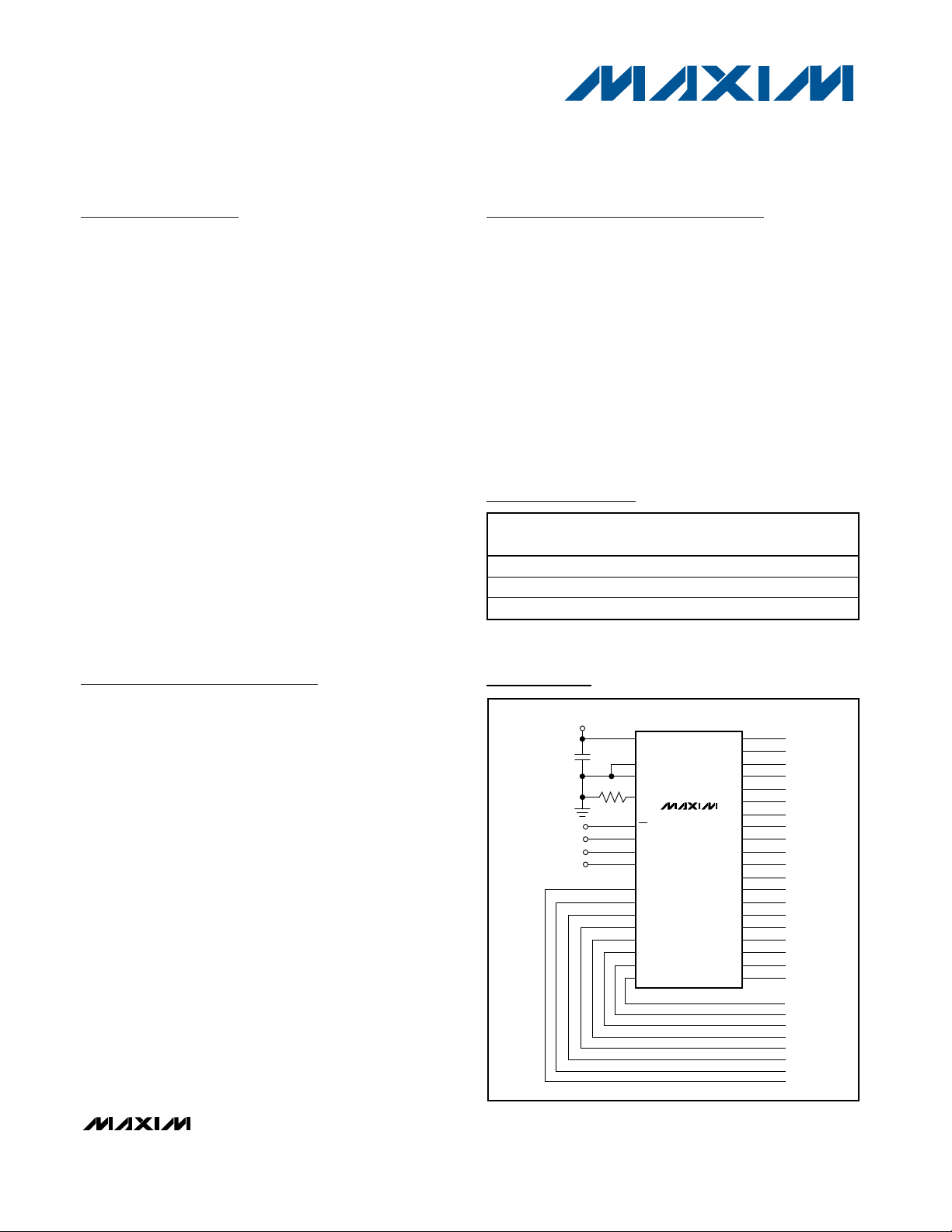
47nF
1
ISET
39kΩ
Typical Operating Circuit
SPI and QSPI are trademarks of Motorola, Inc.
MICROWIRE is a trademark of National Semiconductor Corp.
+Denotes lead-free package.
TEMP RANGE
-40°C to +125°C
-40°C to +125°C
-40°C to +125°C
PACKAGE
MAX7301
4-Wire-Interfaced, 2.5V to 5.5V, 20-Port and
28-Port I/O Expander
2 _______________________________________________________________________________________
ABSOLUTE MAXIMUM RATINGS
Stresses beyond those listed under “Absolute Maximum Ratings” may cause permanent damage to the device. These are stress ratings only, and functional
operation of the device at these or any other conditions beyond those indicated in the operational sections of the specifications is not implied. Exposure to
absolute maximum rating conditions for extended periods may affect device reliability.
(Voltage with respect to GND.)
V+ .............................................................................-0.3V to +6V
All Other Pins................................................-0.3V to (V+ + 0.3V)
P4–P31 Current ................................................................±30mA
GND Current .....................................................................800mA
Continuous Power Dissipation (T
A
= +70°C)
28-Pin SSOP (derate 9.5mW/°C above +70°C) ...........762mW
36-Pin SSOP (derate 11.8mW/°C above +70°C) .........941mW
40-Pin TQFN (derate 26.3mW/°C above +70°C) ....2963.0mW
Operating Temperature Range
(T
MIN
, T
MAX
) ..................................................-40°C to +125°C
Junction Temperature......................................................+150°C
Storage Temperature Range .............................-65°C to +150°C
Lead Temperature (soldering, 10s) .................................+300°C
ELECTRICAL CHARACTERISTICS
(Typical Operating Circuit, V+ = 2.5V to 5.5V, TA= T
MIN
to T
MAX
, unless otherwise noted.) (Note 1)
PARAMETER
SYMBOL
CONDITIONS
MIN
TYP
MAX
UNITS
Operating Supply Voltage V+
5.5 V
TA = +25°C 5.5 8
10Shutdown Supply Current I
SHDN
All digital inputs at V+
or GND
T
A
= T
MIN
to T
MAX
11
µA
TA = +25°C
230
250
Operating Supply Current
(Output High)
I
GPOH
All ports programmed
as outputs high, no
load, all other inputs
at V+ or GND
T
A
= T
MIN
to T
MAX
270
µA
TA = +25°C
210
230
Operating Supply Current
(Output Low)
I
GPOL
All ports programmed
as outputs low, no
load, all other inputs
at V+ or GND
T
A
= T
MIN
to T
MAX
240
µA
TA = +25°C
135
140
Operating Supply Current
(Input)
I
GPI
All ports programmed
as inputs without
pullup, ports, and all
other inputs at V+ or
GND
T
A
= T
MIN
to T
MAX
145
µA
INPUTS AND OUTPUTS
Logic High Input Voltage
Port Inputs
V
IH
0.7 ✕
V+
V
Logic Low Input Voltage
Port Inputs
V
IL
0.3 ✕
V+
V
Input Leakage Current IIH, I
IL
GPIO inputs without pullup,
VPORT = V+ to GND
±1
nA
V+ = 2.5V 12 19 30
GPIO Input Internal Pullup to V+
I
PU
V+ = 5.5V 80
180
µA
Hysteresis Voltage GPIO Inputs
∆V
I
0.3 V
GPIO outputs, I
SOURCE
= 2mA,
T
A
= -40°C to +85°C
V+ -
0.7
Output High Voltage V
OH
GPIO outputs, I
SOURCE
= 1mA,
T
A
= T
MIN
to T
MAX
(Note 2)
V+ -
0.7
V
2.5
TA = - 40° C to + 85°C
180
TA = - 40° C to + 85°C
TA = - 40° C to + 85°C
TA = - 40° C to + 85°C
170
110
-100
120
+100
MAX7301
4-Wire-Interfaced, 2.5V to 5.5V, 20-Port and
28-Port I/O Expander
_______________________________________________________________________________________ 3
Note 1: All parameters tested at TA= +25°C. Specifications over temperature are guaranteed by design.
Note 2: Guaranteed by design.
ELECTRICAL CHARACTERISTICS (continued)
(Typical Operating Circuit, V+ = 2.5V to 5.5V, TA= T
MIN
to T
MAX
, unless otherwise noted.) (Note 1)
PARAMETER
CONDITIONS
UNITS
Port Sink Current I
OL
V
PORT
= 0.6V 2 10 18 mA
Output Short-Circuit Current I
OLSC
Port configured output low, shorted to V+
11
mA
V+ ≤ 3.3V 1.6
Input High-Voltage SCLK, DIN,
CS
V
IH
V+ > 3.3V 2
V
Input Low-Voltage SCLK, DIN,
CS
V
IL
0.6 V
Input Leakage Current SCLK,
DIN, CS
I
IH
, I
IL
-50 +50 nA
Output High-Voltage DOUT V
OH
I
SOURCE
= 1.6mA
V+ -
0.5
V
Output Low-Voltage DOUT V
OL
I
SINK
= 1.6mA 0.4 V
TIMING CHARACTERISTICS (Figure 3)
(V+ = 2.5V to 5.5V, TA= T
MIN
to T
MAX
, unless otherwise noted.) (Note 1)
PARAMETER
CONDITIONS
UNITS
CLK Clock Period t
CP
ns
CLK Pulse Width High t
CH
19 ns
CLK Pulse Width Low t
CL
19 ns
CS Fall to SCLK Rise Setup Time
t
CSS
9.5 ns
CLK Rise to CS Rise Hold Time
t
CSH
0ns
DIN Setup Time t
DS
9.5 ns
DIN Hold Time t
DH
0ns
Output Data Propagation Delay
t
DO
C
LOAD
= 25pF 21 ns
Minimum CS Pulse High t
CSW
19 ns
SYMBOL
SYMBOL
MIN TYP MAX
2.75
MIN TYP MAX
38.4
20.00
MAX7301
4-Wire-Interfaced, 2.5V to 5.5V, 20-Port and
28-Port I/O Expander
4 _______________________________________________________________________________________
OPERATING SUPPLY CURRENT
vs. TEMPERATURE
MAX7301 toc01
TEMPERATURE (°C)
SUPPLY CURRENT (mA)
97.570.042.515.0-12.5
0.04
0.08
0.12
0.16
0.20
0.24
0.28
0.32
0.36
0.40
0
-40.0 125.0
V+ = 2.5V TO 5.5V
NO LOAD
ALL PORTS
OUTPUT (1)
ALL PORTS
OUTPUT (0)
ALL PORTS INPUT HIGH
SHUTDOWN SUPPLY CURRENT
vs. TEMPERATURE
MAX7301 toc02
TEMPERATURE (°C)
SUPPLY CURRENT (µA)
97.570.042.515.0-12.5
4
5
6
7
8
3
-40.0 125.0
V+ = 5.5V
V+ = 3.3V
V+ = 2.5V
OPERATING SUPPLY CURRENT
vs. V+ (OUTPUTS UNLOADED)
MAX7301 toc03
V+ (V)
SUPPLY CURRRENT (mA)
5.04.54.03.53.02.5
1.0
0.1
2.0 5.5
ALL PORTS OUTPUT (1)
ALL PORTS OUTPUT (0)
ALL PORTS INPUT
(PULLUPS DISABLED)
GPO SINK CURRENT vs. TEMPERATURE
(OUTPUT = 0)
MAX7301 toc04
TEMPERATURE (°C)
PORT SINK CURRENT (mA)
97.570.0-12.5 15.0 42.5
4
6
8
10
12
14
16
18
2
-40.0 125.0
V+ = 2.5V TO 5.5V, V
PORT
= 0.6V
GPO SHORT-CIRCUIT CURRENT
vs. TEMPERATURE
MAX7301 toc07
TEMPERATURE (°C)
PORT CURRENT (mA)
97.570.042.515.0-12.5
10
100
1
-40.0 125.0
GPO = 0, PORT
SHORTED TO V+
GPO = 1, PORT
SHORTED TO GND
GPO SOURCE CURRENT vs. TEMPERATURE
(OUTPUT = 1)
MAX7301 toc05
TEMPERATURE (°C)
PORT SOURCE CURRENT (mA)
97.570.042.515.0-12.5
3
4
5
6
7
8
9
2
-40.0 125.0
V
PORT
= 1.4
V+ = 5.5V
V+ = 3.3V
V+ = 2.5V
GPI PULLUP CURRENT
vs. TEMPERATURE
MAX7301 toc06
TEMPERATURE (°C)
PULLUP CURRENT (µA)
97.570.042.515.0-12.5
100
1000
10
-40.0 125.0
V+ = 5.5V
V+ = 3.3V
V+ = 2.5V
__________________________________________Typical Operating Characteristics
(TA = +25°C, unless otherwise noted.)
Detailed Description
The MAX7301 GPIO peripheral provides up to 28 I/O
ports, P4 to P31, controlled through an SPI-compatible
serial interface. The ports can be configured to any
combination of logic inputs and logic outputs, and
default to logic inputs on power-up.
Figure 1 is the MAX7301 functional diagram. Any I/O
port can be configured as a push-pull output (sinking
10mA, sourcing 4.5mA), or a Schmitt-trigger logic
input. Each input has an individually selectable internal
pullup resistor. Additionally, transition detection allows
seven ports (P24 through P30) to be monitored in any
maskable combination for changes in their logic status.
A detected transition is flagged through an interrupt pin
(port P31).
The port configuration registers set the 28 ports, P4 to
P31, individually as GPIO. A pair of bits in registers
0x09 through 0x0F sets each port’s configuration
(Tables 1 and 2).
The 36-pin MAX7301AAX and 40-pin MAX7301ATL
have 28 ports, P4 to P31. The 28-pin MAX7301AAI is
offered in 20 ports, P12 to P31. The eight unused ports
should be configured as outputs on power-up by writing 0x55 to registers 0x09 and 0x0A. If this is not done,
the eight unused ports remain as floating inputs and
quiescent supply current rises, although there is no
damage to the part.
Register Control of I/O Ports
Across Multiple Drivers
The MAX7301 offers 20 or 28 I/O ports, depending on
package choice.
Two addressing methods are available. Any single port
(bit) can be written (set/cleared) at once; or, any
sequence of eight ports can be written (set/cleared) in
any combination at once. There are no boundaries; it is
equally acceptable to write P0 through P7, P1 through
P8, or P31 through P38 (P32 through P38 are nonexistent, so the instructions to these bits are ignored).
Shutdown
When the MAX7301 is in shutdown mode, all ports are
forced to inputs (which can be read), and the pullup
current sources are turned off. Data in the port and
control registers remain unaltered so port configuration
and output levels are restored when the MAX7301 is
taken out of shutdown. The display driver can still be
programmed while in shutdown mode. For minimum
supply current in shutdown mode, logic inputs should
be at GND or V+ potential. Shutdown mode is exited by
setting the S bit in the configuration register (Table 6).
MAX7301
4-Wire-Interfaced, 2.5V to 5.5V, 20-Port and
28-Port I/O Expander
_______________________________________________________________________________________ 5
PIN
36 SSOP
TQFN
NAME FUNCTION
1136 ISET
Bias Current Setting. Connect I
SET
to GND through a resistor (R
ISET
) value of
39kΩ to 120kΩ.
2, 3 2, 3
GND Ground
4440 DOUT 4-Wire Interface Serial Data Output Port
— 5–24 —
I/O Ports. P12 to P31 can be configured as push-pull outputs, CMOS logic
inputs, or CMOS logic inputs with weak pullup resistor.
5–32 —
1–10,
12–19,
21–30
I/O Ports. P4 to P31 can be configured as push-pull outputs, CMOS logic
inputs, or CMOS logic inputs with weak pullup resistor.
——
N.C. No Connection. Not internally connected.
33 25 32 SCLK 4-Wire Interface Serial Clock Input Port
34 26 33 DIN 4-Wire Interface Serial Data Input Port
35 27 34 CS 4-Wire Interface Chip-Select Input, Active Low
36 28 35 V+
Positive Supply Voltage. Bypass V+ to GND with a minimum 0.047µF
——PAD
Exposed
Pad
Exposed Pad on Package Underside. Connect to GND.
Pin Description
28 SSOP
37, 38, 39
P12–P31
P4–P31
11, 20, 31
MAX7301
Serial Interface
The MAX7301 communicates through an SPI-compatible 4-wire serial interface. The interface has three
inputs, Clock (SCLK), Chip Select (CS), and Data In
(DIN), and one output, Data Out (DOUT). CS must be
low to clock data into or out of the device, and DIN
must be stable when sampled on the rising edge of
SCLK. DOUT provides a copy of the bit that was input
15.5 clocks earlier, or upon a query it outputs internal
register data, and is stable on the rising edge of SCLK.
Note that the SPI protocol expects DOUT to be high
impedance when the MAX7301 is not being
accessed; DOUT on the MAX7301 is never high
impedance. See www.maxim-ic.com/an 1879 for
ways to convert DOUT to tri-state, if required.
SCLK and DIN may be used to transmit data to other
peripherals, so the MAX7301 ignores all activity on
SCLK and DIN except between the fall and subsequent
rise of CS.
Control and Operation Using the
4-Wire Interface
Controlling the MAX7301 requires sending a 16-bit
word. The first byte, D15 through D8, is the command
address (Table 3), and the second byte, D7 through
D0, is the data byte (Table 4 through Table 8).
Connecting Multiple MAX7301s
to the 4-Wire Bus
Multiple MAX7301s may be daisy-chained by connecting the DOUT of one device to the DIN of the next, and
driving SCLK and CS lines in parallel (Figure 3). Data at
DIN propagates through the internal shift registers and
appears at DOUT 15.5 clock cycles later, clocked out
on the falling edge of SCLK. When sending commands
to multiple MAX7301s, all devices are accessed at the
same time. An access requires (16 ✕n) clock cycles,
where n is the number of MAX7301s connected together. To update just one device in a daisy-chain, the user
can send the No-Op command (0x00) to the others.
Writing Device Registers
The MAX7301 contains a 16-bit shift register into which
DIN data are clocked on the rising edge of SCLK, when
CS is low. When CS is high, transitions on SCLK have
no effect. When CS goes high, the 16 bits in the Shift
register are parallel loaded into a 16-bit latch. The 16
bits in the latch are then decoded and executed.
4-Wire-Interfaced, 2.5V to 5.5V, 20-Port and
28-Port I/O Expander
6 _______________________________________________________________________________________
Table 1. Port Configuration Map
REGISTER DATA
REGISTER
ADDRESS
CODE (HEX)
D0
Port Configuration for P7, P6, P5, P4 0x09 P7 P6 P5 P4
Port Configuration for P11, P10, P9, P8 0x0A P11 P10 P9 P8
Port Configuration for P15, P14, P13, P12 0x0B P15 P14 P13 P12
Port Configuration for P19, P18, P17, P16 0x0C P19 P18 P17 P16
Port Configuration for P23, P22, P21, P20 0x0D P23 P22 P21 P20
Port Configuration for P27, P26, P25, P24 0x0E P27 P26 P25 P24
Port Configuration for P31, P30, P29, P28 0x0F P31 P30 P29 P28
Table 2. Port Configuration Matrix
PORT
CONFIGURATION
BIT PAIR
MODE
FUNCTION
PORT
REGISTER
(0x20–0x5F)
(0xA0–0xDF)
PIN BEHAVIOR
ADDRESS
)
LOWER
DO NOT USE THIS SETTING
00
Active-low logic output
Output
GPIO Output
Active-high logic output
01
Input
GPIO Input
Without Pullup
Schmitt logic input
10
Input
Register bit =
Schmitt logic input with pullup
11
D7 D6 D5 D4 D3 D2 D1
CODE (HEX
0x09 to 0x0F
Register bit = 0
Register bit = 1
0x09 to 0x0F
UPPER
0x09 to 0x0F
GPIO Input with Pullup
input logic level
0x09 to 0x0F

The MAX7301 is written to using the following
sequence:
1) Take SCLK low.
2) Take CS low. This enables the internal 16-bit shift
register.
3) Clock 16 bits of data into DIN—D15 first, D0 last—
observing the setup and hold times (bit D15 is low,
indicating a write command).
4) Take CS high (either while SCLK is still high after
clocking in the last data bit, or after taking SCLK
low).
5) Take SCLK low (if not already low).
Figure 4 shows a write operation when 16 bits are
transmitted.
It is acceptable to clock more than 16 bits into the
MAX7301 between taking CS low and taking CS high
again. In this case, only the last 16 bits clocked into the
MAX7301 are retained.
Reading Device Registers
Any register data within the MAX7301 may be read by
sending a logic high to bit D15. The sequence is:
1) Take SCLK low.
2) Take CS low (this enables the internal 16-bit Shift
register).
3) Clock 16 bits of data into DIN—D15 first to D0 last.
D15 is high, indicating a read command and bits
D14 through D8 containing the address of the register to be read. Bits D7–D0 contain dummy data,
which is discarded.
4) Take CS high (either while SCLK is still high after
clocking in the last data bit, or after taking SCLK
low), positions D7 through D0 in the Shift register
are now loaded with the register data addressed by
bits D1 through D8.
5) Take SCLK low (if not already low).
6) Issue another read or write command (which can
be a No-Op), and examine the bit stream at DOUT;
the second 8 bits are the contents of the register
addressed by bits D1 through D8 in step 3.
MAX7301
4-Wire-Interfaced, 2.5V to 5.5V, 20-Port and
28-Port I/O Expander
_______________________________________________________________________________________ 7
D0 D1 D2 D3 D4 D5 D6 D7 D8 D9 D10 D11 D12 D13 D14 D15
D0 D1 D2 D3 D4 D5 D6 D7 D8 D9 D10 D11 D12 D13 D14 D15
R/W
8
CEDATA
8
PORT REGISTERS
GPIO
CONFIGURATION
P4 TO P31
GPIO DATA
R/W
CONFIGURATION
REGISTERS
PORT CHANGE
DETECTOR
MASK REGISTER
COMMAND
REGISTER DECODE
8
DATA BYTE COMMAND BYTE
CS
DIN
SCLK
DOUT
8
Figure 1. MAX7301 Functional Diagram

MAX7301
Initial Power-Up
On initial power-up, all control registers are reset, and
the MAX7301 enters shutdown mode (Table 4).
Transition (Port Data Change) Detection
Port transition detection allows any combination of the
seven ports P24–P30 to be continuously monitored for
changes in their logic status (Figure 5). A detected
change is flagged on port P31, which is used as an
active-high interrupt output (INT). Note that the
MAX7301 does not identify which specific port(s)
caused the interrupt, but provides an alert that one or
more port levels have changed.
The mask register contains 7 mask bits that select
which of the seven ports, P24–P30 are to be monitored
(Table 8). Set the appropriate mask bit to enable that
port for transition detect. Clear the mask bit if transitions
on that port are to be ignored. Transition detection
works regardless of whether the port being monitored is
set to input or output, but generally it is not particularly
useful to enable transition detection for outputs.
Port P31 must be configured as an output in order to
work as the interrupt output INT when transition detection is used. Port P31 is set as output by writing bit D7
= 0 and bit D6 = 1 to the port configuration register
(Table 1).
To use transition detection, first set up the mask register and configure port P31 as an output, as described
above. Then enable transition detection by setting the
M bit in the configuration register (Table 7). Whenever
the configuration register is written with the M bit set,
the MAX7301 updates an internal 7-bit snapshot register, which holds the comparison copy of the logic states
of ports P24 through P30. The update action occurs
regardless of the previous state of the M bit, so that it is
not necessary to clear the M bit and then set it again to
update the snapshot register.
When the configuration register is written with the M bit
set, transition detection is enabled and remains
enabled until either the configuration register is written
with the M bit clear, or a transition is detected. The INT
output port P31 goes low, if it was not already low.
Once transition detection is enabled, the MAX7301
continuously compares the snapshot register against
the changing states of P24 through P31. If a change on
any of the monitored ports is detected, even for a short
time (like a pulse), INT output port P31 is latched high.
The INT output is not cleared if more changes occur or
if the data pattern returns to its original snapshot condition. The only way to clear INT is to access (read or
write) the transition detection mask register (Table 8).
Transition detection is a one-shot event. When INT has
been cleared after responding to a transition event,
transition detection is automatically disabled, even
though the M bit in the configuration register remains
set (unless cleared by the user). Reenable transition
detection by writing the configuration register with the
M bit set, to take a new snapshot of the seven ports
P24 to P30.
4-Wire-Interfaced, 2.5V to 5.5V, 20-Port and
28-Port I/O Expander
8 _______________________________________________________________________________________
t
CSH
t
CL
t
CSS
t
CH
t
CSH
CS
SCLK
DIN
DOUT
t
DS
t
DH
t
DO
Figure 2. 4-Wire Interface

External Component R
ISET
The MAX7301 uses an external resistor, R
ISET
, to set
internal biasing. Use a resistor value of 39kΩ.
Applications Information
Low-Voltage Operation
The MAX7301 operates down to 2V supply voltage
(although the sourcing and sinking currents are not
guaranteed), providing that the MAX7301 is powered
up initially to at least 2.5V to trigger the device’s internal
reset, and also that the serial interface is constrained to
10Mbps.
SPI Routing Considerations
The MAX7301’s SPI interface is guaranteed to operate
at 26Mbps on a 2.5V supply, and on a 5V supply typically operates at 50Mbps. This means that transmission
line issues should be considered when the interface
connections are longer than 100mm, particularly with
higher supply voltages. Ringing manifests itself as
communication issues, often intermittent, typically due
to double clocking due to ringing at the SCLK input. Fit
a 1kΩ to 10kΩ parallel termination resistor to either
GND or V+ at the DIN, SCLK, and CS input to damp
ringing for moderately long interface runs. Use lineimpedance matching terminations when making connections between boards.
PC Board Layout Considerations
For the TQFN version, connect the underside exposed
pad to GND. Ensure that all the MAX7301 GND connections are used. A ground plane is not necessary, but
may be useful to reduce supply impedance if the
MAX7301 outputs are to be heavily loaded. Keep the
track length from the ISET pin to the R
ISET
resistor as
short as possible, and take the GND end of the resistor
either to the ground plane or directly to the ground pins.
Power-Supply Considerations
The MAX7301 operates with power-supply voltages of
2.5V to 5.5V. Bypass the power supply to GND with a
0.047µF capacitor as close to the device as possible.
Add a 1µF capacitor if the MAX7301 is far away from
the board’s input bulk decoupling capacitor.
Chip Information
TRANSISTOR COUNT: 30,316
PROCESS: CMOS
MAX7301
4-Wire-Interfaced, 2.5V to 5.5V, 20-Port and
28-Port I/O Expander
_______________________________________________________________________________________ 9
MICROCONTROLLER
SERIAL-DATA OUTPUT
SERIAL CS OUTPUT
SERIA-CLOCK OUTPUT
SERIAL-DATA INPUT
DIN
SCLK
CS
DOUT
DIN
SCLK
CS
DOUT
DIN
SCLK
CS
DOUT
MAX7301
MAX7301
MAX7301
Figure 3. Daisy-Chain Arrangement for Controlling Multiple MAX7301s
.
D15
= 0
D14 D13 D12 D11 D10 D9 D8 D7 D6 D5 D4 D3 D2 D1 D0
D15 = 0
CS
SCLK
DIN
DOUT
Figure 4. Transmission of a16-Bit Write to the MAX7301

MAX7301
4-Wire-Interfaced, 2.5V to 5.5V, 20-Port and
28-Port I/O Expander
10 ______________________________________________________________________________________
Table 3. Register Address Map
COMMAND ADDRESS
REGISTER
HEX
CODE
No-Op
00000 00
0x00
Configuration
00001 00
0x04
Transition Detect Mask
00001 10
0x06
Factory Reserved. Do not write to this.
00001 11
0x07
Port Configuration P7, P6, P5, P4
00010 01
0x09
Port Configuration P11, P10, P9, P8
00010 10
0x0A
Port Configuration P15, P14, P13, P12
00010 11
0x0B
Port Configuration P19, P18, P17, P16
00011 00
0x0C
Port Configuration P23, P22, P21, P20
00011 01
0x0D
Port Configuration P27, P26, P25, P24
00011 10
0x0E
Port Configuration P31, P30, P29, P28
00011 11
0x0F
Port 0 only (virtual port, no action)
01000 00
0x20
Port 1 only (virtual port, no action)
01000 01
0x21
Port 2 only (virtual port, no action)
01000 10
0x22
Port 3 only (virtual port, no action)
01000 11
0x23
Port 4 only (data bit D0. D7–D1 read as 0)
01001 00
0x24
Port 5 only (data bit D0. D7–D1 read as 0)
01001 01
0x25
Port 6 only (data bit D0. D7–D1 read as 0)
01001 10
0x26
Port 7 only (data bit D0. D7–D1 read as 0)
01001 11
0x27
Port 8 only (data bit D0. D7–D1 read as 0)
01010 00
0x28
Port 9 only (data bit D0. D7–D1 read as 0)
01010 01
0x29
Port 10 only (data bit D0. D7–D1 read as 0)
01010 10
0x2A
Port 11 only (data bit D0. D7–D1 read as 0)
01010 11
0x2B
Port 12 only (data bit D0. D7–D1 read as 0)
01011 00
0x2C
Port 13 only (data bit D0. D7–D1 read as 0)
01011 01
0x2D
Port 14 only (data bit D0. D7–D1 read as 0)
01011 10
0x2E
Port 15 only (data bit D0. D7–D1 read as 0)
01011 11
0x2F
Port 16 only (data bit D0. D7–D1 read as 0)
01100 00
0x30
Port 17 only (data bit D0. D7–D1 read as 0)
01100 01
0x31
Port 18 only (data bit D0. D7–D1 read as 0)
01100 10
0x32
Port 19 only (data bit D0. D7–D1 read as 0)
01100 11
0x33
Port 20 only (data bit D0. D7–D1 read as 0)
01101 00
0x34
Port 21 only (data bit D0. D7–D1 read as 0)
01101 01
0x35
Port 22 only (data bit D0. D7–D1 read as 0)
01101 10
0x36
Port 23 only (data bit D0. D7–D1 read as 0)
01101 11
0x37
Port 24 only (data bit D0. D7–D1 read as 0)
01110 00
0x38
Port 25 only (data bit D0. D7–D1 read as 0)
01110 01
0x39
D15 D14 D13 D12 D11 D10 D9 D8
R/W
R/W
R/W
R/W
R/W
R/W
R/W
R/W
R/W
R/W
R/W
R/W
R/W
R/W
R/W
R/W
R/W
R/W
R/W
R/W
R/W
R/W
R/W
R/W
R/W
R/W
R/W
R/W
R/W
R/W
R/W
R/W
R/W
R/W
R/W
R/W
R/W

MAX7301
4-Wire-Interfaced, 2.5V to 5.5V, 20-Port and
28-Port I/O Expander
______________________________________________________________________________________ 11
COMMAND ADDRESS
REGISTER
HEX
CODE
Port 26 only (data bit D0. D7–D1 read as 0)
0111010
0x3A
Port 27 only (data bit D0. D7–D1 read as 0)
0111011
0x3B
Port 28 only (data bit D0. D7–D1 read as 0)
0111100
0x3C
Port 29 only (data bit D0. D7–D1 read as 0)
0111101
0x3D
Port 30 only (data bit D0. D7–D1 read as 0)
0111110
0x3E
Port 31 only (data bit D0. D7–D1 read as 0)
0111111
0x3F
4 ports 4–7 (data bits D0–D3. D4–D7 read as 0)
1000000
0x40
5 ports 4–8 (data bits D0–D4. D5–D7 read as 0)
1000001
0x41
6 ports 4–9 (data bits D0–D5. D6–D7 read as 0)
1000010
0x42
7 ports 4–10 (data bits D0–D6. D7 reads as 0)
1000011
0x43
8 ports 4–11 (data bits D0–D7)
1000100
0x44
8 ports 5–12 (data bits D0–D7)
1000101
0x45
8 ports 6–13 (data bits D0–D7)
1000110
0x46
8 ports 7–14 (data bits D0–D7)
1000111
0x47
8 ports 8–15 (data bits D0–D7)
1001000
0x48
8 ports 9–16 (data bits D0–D7)
1001001
0x49
8 ports 10–17 (data bits D0–D7)
1001010
0x4A
8 ports 11–18 (data bits D0–D7)
1001011
0x4B
8 ports 12–19 (data bits D0–D7)
1001100
0x4C
8 ports 13–20 (data bits D0–D7)
1001101
0x4D
8 ports 14–21 (data bits D0–D7)
1001110
0x4E
8 ports 15–22 (data bits D0–D7)
1001111
0x4F
8 ports 16–23 (data bits D0–D7)
1010000
0x50
8 ports 17–24 (data bits D0–D7)
1010001
0x51
8 ports 18–25 (data bits D0–D7)
1010010
0x52
8 ports 19–26 (data bits D0–D7)
1010011
0x53
8 ports 20–27 (data bits D0–D7)
1010100
0x54
8 ports 21–28 (data bits D0–D7)
1010101
0x55
8 ports 22–29 (data bits D0–D7)
1010110
0x56
8 ports 23–30 (data bits D0–D7)
1010111
0x57
8 ports 24–31 (data bits D0–D7)
1011000
0x58
7 ports 25–31 (data bits D0–D6. D7 reads as 0)
1011001
0x59
6 ports 26–31 (data bits D0–D5. D6–D7 read as 0)
1011010
0x5A
5 ports 27–31 (data bits D0–D4. D5–D7 read as 0)
1011011
0x5B
4 ports 28–31 (data bits D0–D3. D4–D7 read as 0)
1011100
0x5C
3 ports 29–31 (data bits D0–D2. D3–D7 read as 0)
1011101
0x5D
2 ports 30–31 (data bits D0–D1. D2–D7 read as 0)
1011110
0x5E
1 port 31 only (data bit D0. D1–D7 read as 0)
1011111
0x5F
Table 3. Register Address Map (continued)
Note: Unused bits read as 0.
D15 D14 D13 D12 D11 D10 D9 D8
R/W
R/W
R/W
R/W
R/W
R/W
R/W
R/W
R/W
R/W
R/W
R/W
R/W
R/W
R/W
R/W
R/W
R/W
R/W
R/W
R/W
R/W
R/W
R/W
R/W
R/W
R/W
R/W
R/W
R/W
R/W
R/W
R/W
R/W
R/W
R/W
R/W
R/W

MAX7301
4-Wire-Interfaced, 2.5V to 5.5V, 20-Port and
28-Port I/O Expander
GPIO INPUT
CONDITIONING
P31
P30
P29
P28
P27
P26
P25
P24
GPIO/PORT OUTPUT LATCH
GPIO INPUT
CONDITIONING
GPIO/PORT OUTPUT LATCH
GPIO INPUT
CONDITIONING
GPIO/PORT OUTPUT LATCH
GPIO INPUT
CONDITIONING
GPIO/PORT OUTPUT LATCH
GPIO INPUT
CONDITIONING
GPIO/PORT OUTPUT LATCH
GPIO INPUT
CONDITIONING
GPIO/PORT OUTPUT LATCH
GPIO INPUT
CONDITIONING
GPIO/PORT OUTPUT LATCH
D Q
D Q
D Q
D Q
D Q
D Q
D Q
CLOCK PULSE WHEN WRITING CONFIGURATION REGISTER WITH M BIT SET
OR
CONFIGURATION REGISTER M BIT = SET
R
S
GPIO IN
GPIO/PORT OUT
CLOCK PULSE AFTER EACH READ ACCESS TO MASK REGISTER
MASK REGISTER BIT 6
MASK REGISTER BIT 5
MASK REGISTER BIT 4
MASK REGISTER BIT 3
MASK REGISTER BIT 2
MASK REGISTER BIT 1
MASK REGISTER LSB
GPIO IN
GPIO/PORT OUT
GPIO IN
GPIO/PORT OUT
GPIO IN
GPIO/PORT OUT
GPIO IN
GPIO/PORT OUT
GPIO IN
GPIO/PORT OUT
GPIO IN
GPIO/PORT OUT
GPIO IN
GPIO/PORT OUT
GPIO INPUT
CONDITIONING
GPIO/PORT
OUTPUT LATCH
INT
OUTPUT LATCH
Figure 5. Maskable GPIO Ports P24 Through P31
12 ______________________________________________________________________________________

MAX7301
4-Wire-Interfaced, 2.5V to 5.5V, 20-Port and
28-Port I/O Expander
______________________________________________________________________________________ 13
Table 4. Power-Up Configuration
REGISTER DATA
REGISTER
FUNCTION
POWER-UP CONDITION
ADDRESS
)
D0
Port Register
Bits 4 to 31
GPIO Output Low
0x24 to
0x3F
0
Configuration
Register
Shutdown Enabled
Transition Detection Disabled
0x04
0
Input Mask
Register
All Clear (Masked Off) 0x06
0
Port
Configuration
P7, P6, P5, P4: GPIO Inputs Without Pullup 0x09
0
Port
Configuration
P11, P10, P9, P8: GPIO Inputs Without Pullup 0x0A
0
Port
Configuration
P15, P14, P13, P12: GPIO Inputs Without
Pullup
0x0B
0
Port
Configuration
P19, P18, P17, P16: GPIO Inputs Without
Pullup
0x0C
0
Port
Configuration
P23, P22, P21, P20: GPIO Inputs Without
Pullup
0x0D
0
Port
Configuration
P27, P26, P25, P24: GPIO Inputs Without
Pullup
0x0E
0
Port
Configuration
P31, P30, P29, P28: GPIO Inputs Without
Pullup
0x0F
0
X = Unused bits; if read, zero results.
Table 5. Configuration Register Format
REGISTER DATA
FUNCTION
ADDRESS CODE
(HEX)
D7 D6 D5 D4 D3 D2 D1 D0
Configuration Register
0x04 M 0 XXXXXS
Table 6. Shutdown Control (S Data Bit D0) Format
REGISTER DATA
FUNCTION
ADDRESS CODE
(HEX)
D7 D6 D5 D4 D3 D2 D1 D0
Shutdown 0x04 M 0 XXXXX0
Normal Operation 0x04 M 0 XXXXX1
CODE (HEX
D7 D6 D5 D4 D3 D2 D1
XXXXXXX
00XXXXX
X000000
1010101
1010101
1010101
1010101
1010101
1010101
1010101

MAX7301
4-Wire-Interfaced, 2.5V to 5.5V, 20-Port and
28-Port I/O Expander
14 ______________________________________________________________________________________
Table 8. Transition Detection Mask Register
REGISTER DATA
FUNCTION
REGISTER
ADDRESS
(HEX)
READ/
D7 D6 D5 D4 D3 D2 D1 D0
Read 0
Mask
Register
0x06
Write
Port
30
Port
29
Port
28
Port
27
Port
26
Port
25
Port
24
mask
Table 7. Transition Detection Control (M Data Bit D7) Format
REGISTER DATA
FUNCTION
ADDRESS CODE
(HEX)
D7 D6 D5 D4 D3 D2 D1 D0
Disabled 0x04 0 0 XXXXXS
Enabled 0x04 1 0 XXXXXS
WRITE
Unchanged
mask
mask
mask
mask
mask
mask

TOP VIEW
36
35
34
33
32
31
30
29
28
27
26
25
24
23
1
2
3
4
5
6
7
8
9
10
11
12
13
14
V+
CS
DIN
SCLK
P4
P31
P26
P5
P30
P6
P29
P7
P28
P27
P17
P16
P15
P11
P14
P10
P13
P9
P12
P8
DOUT
GND
GND
ISET
36 SSOP
MAX7301
22
21
20
19
15
16
17
18 P22
P25
P24
P23
P21
P20
P19
P18
28
27
26
25
24
23
22
21
20
19
18
17
16
15
1
2
3
4
5
6
7
8
9
10
11
12
13
14
V+
CS
DIN
SCLK
P31
P30
P22
P29
P28
P27
P26
P25
P24
P23
P21
P20
P19
P18
P17
P16
P15
P14
P13
P12
DOUT
GND
GND
ISET
28 SSOP
MAX7301
+
+
+
N.C.
P25
P23
P22
P19
P18
N.C.
P21
P20
P24
P4
P31
P30
P6
P28
P27
P26
P29
P7
P5
DIN
CS
V+
ISET
GND
GND
GND
DOUT
12345678910
30 29 28 27 26 25 24 23 22 21
SCLK
N.C.
P9
P13
P10
P14
P11
P15
P16
P17
P12
P8
31
32
33
34
35
36
37
38
39
40
20
19
18
17
16
15
14
13
12
11
TQFN
MAX7301
MAX7301
4-Wire-Interfaced, 2.5V to 5.5V, 20-Port and
28-Port I/O Expander
______________________________________________________________________________________ 15
Pin Configurations

MAX7301
4-Wire-Interfaced, 2.5V to 5.5V, 20-Port and
28-Port I/O Expander
16 ______________________________________________________________________________________
SSOP.EPS
PACKAGE OUTLINE, 36L SSOP, 0.80 MM PITCH
1
1
21-0040 E
REV.DOCUMENT CONTROL NO.APPROVAL
PROPRIETARY INFORMATION
TITLE:
FRONT VIEW
MAX
0.011
0.104
0.017
0.299
0.013
INCHES
0.291
0.009
E
C
DIM
0.012
0.004
B
A1
MIN
0.096A
0.23
7.40 7.60
0.32
MILLIMETERS
0.10
0.30
2.44
MIN
0.44
0.29
MAX
2.65
0.040
0.020L
0.51 1.02
H 0.4140.398 10.11 10.51
e 0.0315 BSC 0.80 BSC
D 0.6120.598
15.20 15.55
HE
A1
A
D
e
B
0∞-8∞
L
C
TOP VIEW
SIDE VIEW
1
36
SSOP.EPS
PACKAGE OUTLINE, SSOP, 5.3 MM
1
1
21-0056
C
REV.DOCUMENT CONTROL NO.APPROVAL
PROPRIETARY INFORMATION
TITLE:
NOTES:
1. D&E DO NOT INCLUDE MOLD FLASH.
2. MOLD FLASH OR PROTRUSIONS NOT TO EXCEED .15 MM (.006").
3. CONTROLLING DIMENSION: MILLIMETERS.
4. MEETS JEDEC MO150.
5. LEADS TO BE COPLANAR WITHIN 0.10 MM.
7.90
H
L
0∞
0.301
0.025
8∞
0.311
0.037
0∞
7.65
0.63
8∞
0.95
MAX
5.38
MILLIMETERS
B
C
D
E
e
A1
DIM
A
SEE VARIATIONS
0.0256 BSC
0.010
0.004
0.205
0.002
0.015
0.008
0.212
0.008
INCHES
MIN
MAX
0.078
0.65 BSC
0.25
0.09
5.20
0.05
0.38
0.20
0.21
MIN
1.73 1.99
MILLIMETERS
6.07
6.07
10.07
8.07
7.07
INCHES
D
D
D
D
D
0.239
0.239
0.397
0.317
0.278
MIN
0.249
0.249
0.407
0.328
0.289
MAX
MIN
6.33
6.33
10.33
8.33
7.33
14L
16L
28L
24L
20L
MAX
N
A
D
e
A1
L
C
HE
N
12
B
0.068
Package Information
(The package drawing(s) in this data sheet may not reflect the most current specifications. For the latest package outline information,
go to www.maxim-ic.com/packages
.)

MAX7301
4-Wire-Interfaced, 2.5V to 5.5V, 20-Port and
28-Port I/O Expander
Maxim cannot assume responsibility for use of any circuitry other than circuitry entirely embodied in a Maxim product. No circuit patent licenses are
implied. Maxim reserves the right to change the circuitry and specifications without notice at any time.
Maxim Integrated Products, 120 San Gabriel Drive, Sunnyvale, CA 94086 408-737-7600 ____________________ 17
© 2006 Maxim Integrated Products Printed USA is a registered trademark of Maxim Integrated Products, Inc.
Package Information (continued)
(The package drawing(s) in this data sheet may not reflect the most current specifications. For the latest package outline information,
go to www.maxim-ic.com/packages
.)
e
E
2
E/
D/2
(ND-1) X
D
e
L1
A
A1 A2
e
e
L
(NE-1) X
L
k
C
L
e e
PROPRIETARY INFORMATION
TITLE:
APPROVAL
k
D2/2
E2/2
C
L
E2
PACKAGE OUTLINE
36, 40, 48L THIN QFN, 6x6x0.8m
DOCUMENT CONTROL NO.
21-0141
QFN THIN.EPS
C
D2
L
b
C
L
LL
m
REV.
1
F
2
NOTES:
1. DIMENSIONING & TOLERANCING CONFORM TO ASME Y14.5M-1994.
2. ALL DIMENSIONS ARE IN MILLIMETERS. ANGLES ARE IN DEGREES.
3. N IS THE TOTAL NUMBER OF TERMINALS.
4. THE TERMINAL #1 IDENTIFIER AND TERMINAL NUMBERING CONVENTION SHALL CONFORM TO JESD 95-1
SPP-012. DETAILS OF TERMINAL #1 IDENTIFIER ARE OPTIONAL, BUT MUST BE LOCATED WITHIN THE
ZONE INDICATED. THE TERMINAL #1 IDENTIFIER MAY BE EITHER A MOLD OR MARKED FEATURE.
5. DIMENSION b APPLIES TO METALLIZED TERMINAL AND IS MEASURED BETWEEN 0.25 mm AND 0.30 mm
FROM TERMINAL TIP.
6. ND AND NE REFER TO THE NUMBER OF TERMINALS ON EACH D AND E SIDE RESPECTIVELY.
7. DEPOPULATION IS POSSIBLE IN A SYMMETRICAL FASHION.
8. COPLANARITY APPLIES TO THE EXPOSED HEAT SINK SLUG AS WELL AS THE TERMINALS.
9. DRAWING CONFORMS TO JEDEC MO220, EXCEPT FOR 0.4mm LEAD PITCH PACKAGE T4866-1.
10. WARPAGE SHALL NOT EXCEED 0.10
11. MARKING IS FOR PACKAGE ORIENTATION REFERENCE ONLY.
12. NUMBER OF LEADS SHOWN FOR REFERENCE
mm.
ONLY.
PROPRIETARY INFORMATION
TITLE:
PACKAGE OUTLINE
36, 40, 48L THIN QFN, 6x6x0.8mm
APPROVAL
DOCUMENT CONTROL NO.
21-0141
REV.
2
F
2
 Loading...