

Page 1
现货库存、技术资料、百科信息、热点资讯,精彩尽在鼎好!
General Description
The MAX7300 compact, serial-interfaced, I/O expansion peripheral provides microprocessors with up to 28
ports. Each port is individually user configurable to
either a logic input or logic output.
Each port can be configured as either a push-pull logic
output capable of sinking 10mA and sourcing 4.5mA, or a
Schmitt logic input with optional internal pullup. Seven
ports feature configurable transition detection logic, which
generates an interrupt upon change of port logic level.
The MAX7300 is controlled through an I2C™-compatible
2-wire serial interface, and uses four-level logic to allow
16 I2C addresses from only two select pins.
The MAX7300AAX and MAX7300AGL have 28 ports
and are available in 36-pin SSOP and 40-pin QFN packages, respectively. The MAX7300AAI and MAX7300ANI
have 20 ports and are available in 28-pin SSOP and 28pin DIP packages, respectively.
Applications
White Goods Industrial Controllers
Automotive System Monitoring
Features
♦ 400kbps I2C-Compatible Serial Interface
♦ 2.5V to 5.5V Operation
♦ -40°C to +125°C Temperature Range
♦ 20 or 28 I/O Ports, Each Configurable as
Push-Pull Logic Output
Schmitt Logic Input
Schmitt Logic Input with Internal Pullup
♦ 11µA (max) Shutdown Current
♦ Logic Transition Detection for Seven I/O Ports
MAX7300
2-Wire-Interfaced, 2.5V to 5.5V, 20-Port or
28-Port I/O Expander
________________________________________________________________ Maxim Integrated Products 1
19-2413; Rev 1; 2/03
For pricing, delivery, and ordering information, please contact Maxim/Dallas Direct! at
1-888-629-4642, or visit Maxim’s website at www.maxim-ic.com.
Ordering Information
I2C is a trademark of Philips Corp.
P5
P4
P7
P8
P6
P10
P9
P12
P13
P11
P15
P14
P17
P18
P16
P20
P19
I/O 5
I/O 4
I/O 7
I/O 8
I/O 6
I/O 10
I/O 9
I/O 12
I/O 13
I/O 11
I/O 15
I/O 14
I/O 17
I/O 18
I/O 16
I/O 20
I/O 19
I/O 21
I/O 22
I/O 23
P22
P23
P21
36
2
3
4
33
35
34
29
27
31
24
25
22
21
23
V+
GND
GND
AD0
AD1
SCL
P30
P29
P31
P27
P28
P25
P24
P26
32
30
26
5
7
9
28
6
8
11
10
12
14
15
13
17
16
19
20
18
SDA
MAX7300AAX
3V
DATA
CLOCK
I/O 24
I/O 25
I/O 27
I/O 26
I/O 29
I/O 30
I/O 28
I/O 31
47nF
39kΩ
1
ISET
Typical Operating Circuit
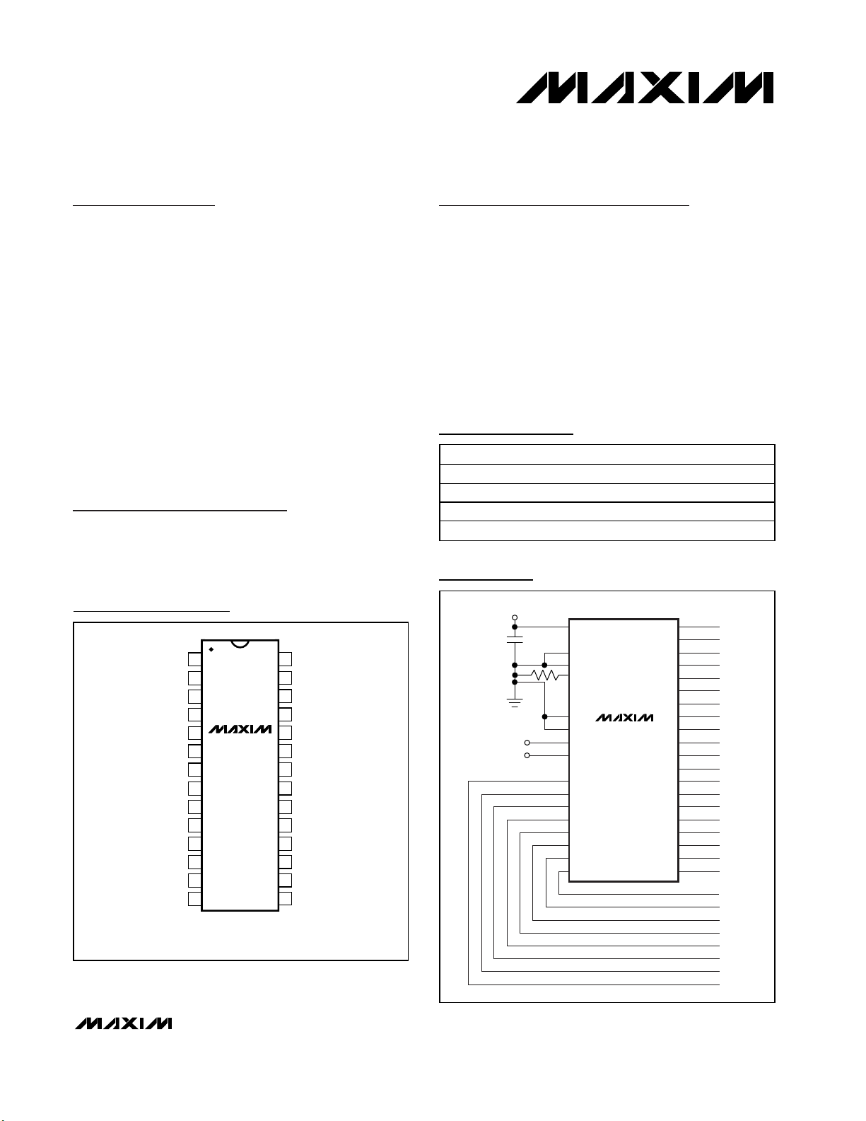
Pin Configurations
Pin Configurations continued at end of data sheet.
PART TEMP RANGE PIN-PACKAGE
MAX7300ANI -40°C to +125°C 28 DIP
MAX7300AAI -40°C to +125°C 28 SSOP
MAX7300AAX -40°C to +125°C 36 SSOP
MAX7300AGL -40°C to +125°C 40 QFN
TOP VIEW
ISET
1
GND
2
GND
3
AD0
4
P12
5
P13
6
P14
7
P15
8
P16
9
P17
10
P18
11
P19
12
P20
13
P21
14
MAX7300
SSOP/DIP
28
27
26
25
24
23
22
21
20
19
18
17
16
15
V+
AD1
SCL
SDA
P31
P30
P29
P28
P27
P26
P25
P24
P23
P22
Page 2
MAX7300
2-Wire-Interfaced, 2.5V to 5.5V, 20-Port or
28-Port I/O Expander
2 _______________________________________________________________________________________
ABSOLUTE MAXIMUM RATINGS
Stresses beyond those listed under “Absolute Maximum Ratings” may cause permanent damage to the device. These are stress ratings only, and functional
operation of the device at these or any other conditions beyond those indicated in the operational sections of the specifications is not implied. Exposure to
absolute maximum rating conditions for extended periods may affect device reliability.
Voltage (with respect to GND)
V+ .............................................................................-0.3V to +6V
SCL, SDA, AD0, AD1................................................-0.3V to +6V
All Other Pins................................................-0.3V to (V+ + 0.3V)
P4–P31 Current ................................................................±30mA
GND Current .....................................................................800mA
Continuous Power Dissipation (T
A
= +70°C)
28-Pin PDIP (derate 20.8mW/°C above +70°C).........1667mW
28-Pin SSOP (derate 9.5mW/°C above +70°C) ...........762mW
36-Pin SSOP (derate 11.8mW/°C above +70°C) .........941mW
40-Pin QFN (derate 23.25mW/°C aboveT
A
= +70°C)..1860mW
Operating Temperature Range
(T
MIN
to T
MAX
) ...............................................-40°C to +125°C
Junction Temperature......................................................+150°C
Storage Temperature Range .............................-65°C to +150°C
Lead Temperature (soldering, 10s) .................................+300°C
ELECTRICAL CHARACTERISTICS
(Typical Operating Circuit, V+ = 2.5V to 5.5V, TA= T
MIN
to T
MAX
, unless otherwise noted.) (Note 1)
Operating Supply Voltage V+ 2.5 5.5 V
Operating Supply Current I
PARAMETER SYMBOL CONDITIONS MIN TYP MAX UNITS
I
SHDN
GPOH
All digital inputs at
V+ or GND
All ports programmed
as outputs high, no
load, all other inputs
at V+ or GND
TA = +25°C 5.5 8
TA = -40°C to +85°C10Shutdown Supply Current
to T
T
MIN
TA = +25°C 180 240
TA = -40°C to +85°C 260
to T
T
MIN
MAX
MAX
11
280
µA
µA
All ports programmed
Operating Supply Current I
Operating Supply Current I
INPUTS AND OUTPUTS
Logic High Input Voltage
Port Inputs
Logic Low Input Voltage
Port Inputs
Input Leakage Current IIH, I
GPIO Input Internal Pullup to V+ I
Hysteresis Voltage GPIO Inputs ∆V
GPOL
GPI
V
V
as outputs low, no
load, all other inputs
at V+ or GND
All ports programmed
as inputs without
pullup, ports, and all
other inputs at V+ or
GND
IH
IL
GPIO inputs without pullup,
IL
PU
I
= V+ to GND
V
PORT
V+ = 2.5V 12 19 30
V+ = 5.5V 80 120 180
TA = +25°C 170 210
TA = -40°C to +85°C 230
T
to T
MIN
MAX
TA = +25°C 110 135
TA = -40°C to +85°C 140
to T
T
MIN
MAX
0.7 x
V+
-100 ±1 +100 nA
0.3 V
240
145
0.3 x
V+
µA
µA
V
V
µA
Page 3
MAX7300
2-Wire-Interfaced, 2.5V to 5.5V, 20-Port or
28-Port I/O Expander
_______________________________________________________________________________________ 3
ELECTRICAL CHARACTERISTICS (continued)
(Typical Operating Circuit, V+ = 2.5V to 5.5V, TA= T
MIN
to T
MAX
, unless otherwise noted.) (Note 1)
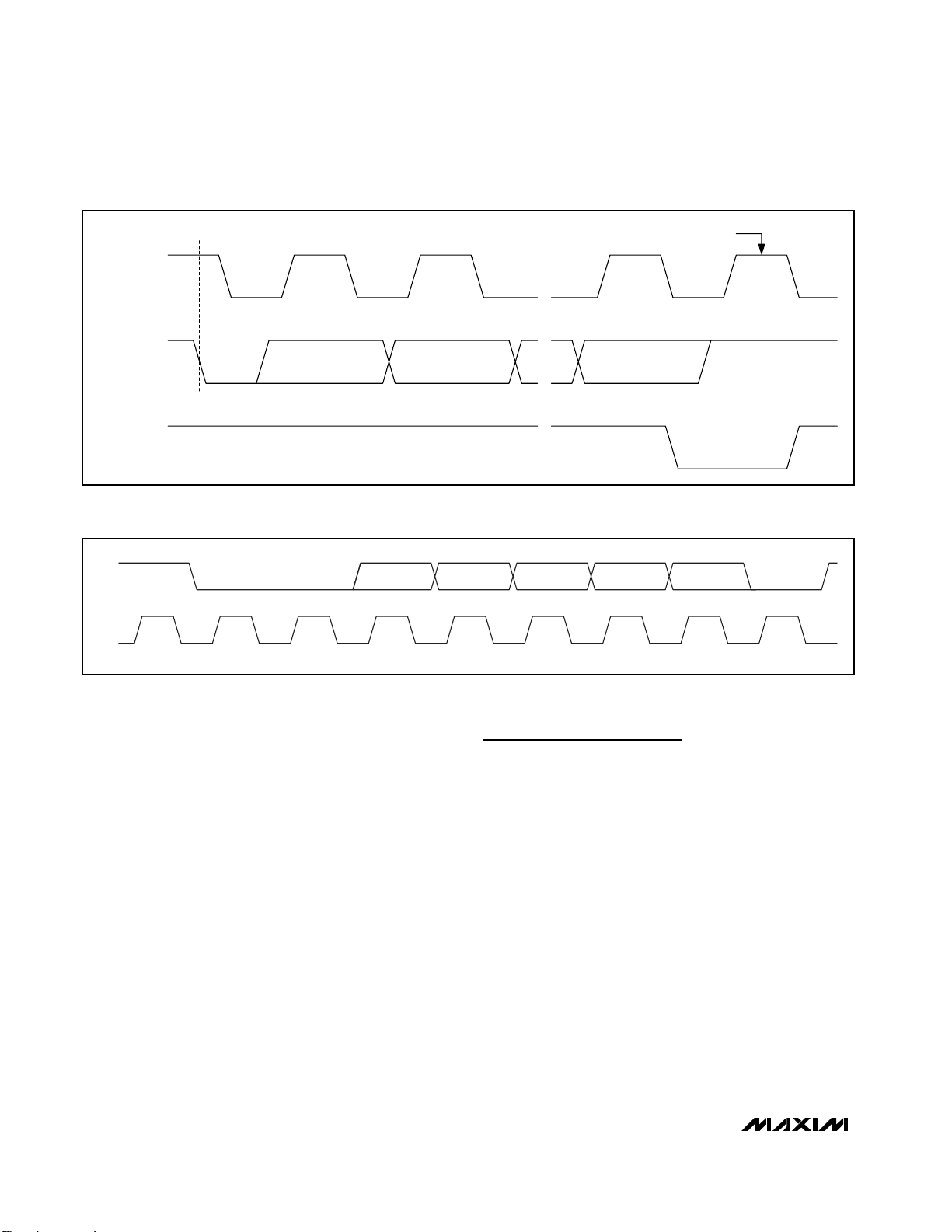
TIMING CHARACTERISTICS (Figure 2)
(V+ = 2.5V to 5.5V, TA= T
MIN
to T
MAX
, unless otherwise noted.) (Note 1)
Output High Voltage V
Port Sink Current I
Output Short-Circuit Current I
Input High-Voltage SDA, SCL,
AD0, AD1
Input Low-Voltage SDA, SCL,
AD0, AD1
Input Leakage Current SDA, SCL IIH, I
PARAMETER SYMBOL CONDITIONS MIN TYP MAX UNITS
OH
OL
OLSC
V
IH
V
IL
IL
Input Capacitance (Note 2) 10 pF
Output Low-Voltage SDA V
OL
GPIO outputs, I
T
= -40°C to +85°C
A
GPIO outputs, I
= T
T
A
MIN
V
= 0.6V 2 10 18 mA
PORT
= 2mA,
SOURCE
= 1mA,
SOURCE
to T
MAX
(Note 2)
V+ -
0.7
V+ -
0.7
Port configured output low, shorted to V+ 2.75 11 20 mA
0.7 x
V+
0.3 x
V+
-50 +50 nA
I
= 6mA 0.4 V
SINK
PARAMETER SYMBOL CONDITIONS MIN TYP MAX UNITS
Serial Clock Frequency f
Bus Free Time Between a STOP
and a START Condition
Hold Time (Repeated) START
Condition
Repeated START Condition
Setup Time
STOP Condition Setup Time t
Data Hold Time t
Data Setup Time t
SCL Clock Low Period t
SCL Clock High Period t
Rise Time of Both SDA and SCL
Signals, Receiving
Fall Time of Both SDA and SCL
Signals, Receiving
Fall Time of SDA Transmitting t
Pulse Width of Spike Suppressed t
Capacitive Load for Each Bus
Line
SCL
t
BUF
t
HD, STA
t
SU, STA
SU, STO
HD, DAT
SU, DAT
LOW
HIGH
F,TX
C
(Note 3) 15 900 ns
(Notes 2, 4)
t
R
(Notes 2, 4)
t
F
(Notes 2, 5)
(Notes 2, 6) 0 50 ns
SP
(Note 2) 400 pF
b
400 kHz
1.3 µs
0.6 µs
0.6 µs
0.6 µs
100 ns
1.3 µs
0.7 µs
20 +
0.1C
20 +
0.1C
20 +
0.1C
b
b
b
300 ns
300 ns
250 ns
V
V
V
Page 4
MAX7300
2-Wire-Interfaced, 2.5V to 5.5V, 20-Port or
28-Port I/O Expander
4 _______________________________________________________________________________________
__________________________________________Typical Operating Characteristics
(R
ISET
= 39kΩ, TA = +25°C, unless otherwise noted.)
TIMING CHARACTERISTICS (Figure 2) (continued)
(V+ = 2.5V to 5.5V, TA= T
MIN
to T
MAX
, unless otherwise noted.) (Note 1)
Note 1: All parameters tested at T
A
= +25°C. Specifications over temperature are guaranteed by design.
Note 2: Guaranteed by design.
Note 3: A master device must provide a hold time of at least 300ns for the SDA signal (referred to V
IL
of the SCL signal) in order to
bridge the undefined region of SCL’s falling edge.
Note 4: C
b
= total capacitance of one bus line in pF. tRand tFmeasured between 0.3V+ and 0.7V+.
Note 5: I
SINK
≤ 6mA. Cb= total capacitance of one bus line in pF. tRand tFmeasured between 0.3V+ and 0.7V+.
Note 6: Input filters on the SDA and SCL inputs suppress noise spikes less than 50ns.
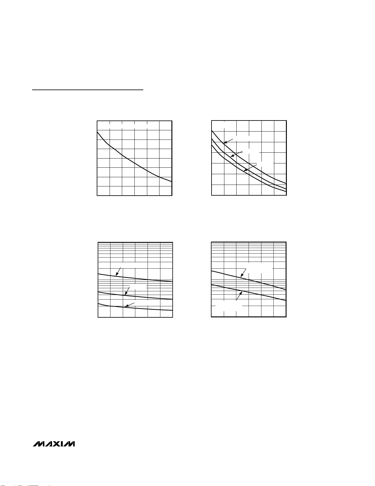
OPERATING SUPPLY CURRENT
vs. TEMPERATURE
0.40
V+ = 2.5V TO 5.5V
0.36
NO LOAD
0.32
0.28
ALL PORTS
OUTPUT (1)
0.24
0.20
0.16
0.12
SUPPLY CURRENT (mA)
0.08
0.04
0
-40.0 125.0
TEMPERATURE (°C)
ALL PORTS
OUTPUT (0)
ALL PORTS INPUT HIGH
MAX7300 toc01
SUPPLY CURRENT (µA)
97.570.042.515.0-12.5
SHUTDOWN SUPPLY CURRENT
vs. TEMPERATURE
8
7
V+ = 3.3V
6
5
4
3
-40.0 125.0
V+ = 5.5V
V+ = 2.5V
97.570.042.515.0-12.5
TEMPERATURE (°C)
1
MAX7300 toc02
SUPPLY CURRENT ( mA)
0.1
OPERATING SUPPLY CURRENT vs. V+
(OUTPUTS UNLOADED)
ALL PORTS OUTPUT (1)
ALL PORTS OUTPUT (0)
ALL PORTS INPUT
(PULLUPS DISABLED)
2.0 5.5
V+ (V)
5.04.54.03.53.02.5
MAX7300 toc03
Page 5
MAX7300
2-Wire-Interfaced, 2.5V to 5.5V, 20-Port or
28-Port I/O Expander
_______________________________________________________________________________________ 5
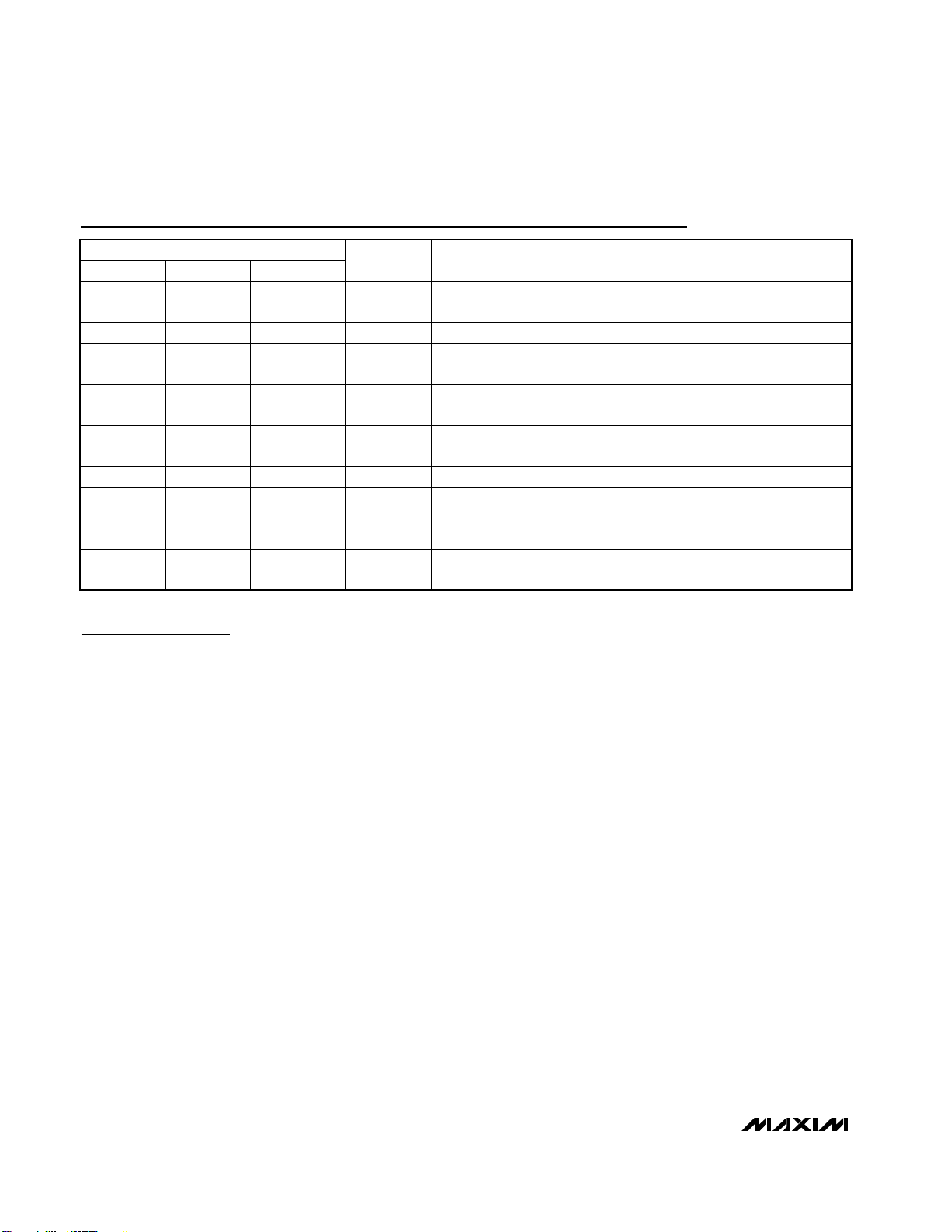
Typical Operating Characteristics (continued)
(R
ISET
= 39kΩ, TA = +25°C, unless otherwise noted.)
GPO SINK CURRENT vs. TEMPERATURE
18
V+ = 2.5V TO 5.5V, V
16
14
12
10
8
PORT SINK CURRENT (mA)
6
4
2
-40.0 125.0
GPI PULLUP CURRENT
1000
100
PULLUP CURRENT (µA)
10
-40.0 125.0
(OUTPUT = 0)
= 0.6V
PORT
TEMPERATURE (°C)
vs. TEMPERATURE
V+ = 5.5V
V+ = 3.3V
V+ = 2.5V
TEMPERATURE (°C)
GPO SOURCE CURRENT vs. TEMPERATURE
9
V
PORT
MAX7300 toc04
97.570.0-12.5 15.0 42.5
MAX7300 toc06
97.570.042.515.0-12.5
8
7
6
5
4
PORT SOURCE CURRENT (mA)
3
2
-40.0 125.0
100
10
PORT CURRENT (mA)
SHORTED TO GND
1
-40.0 125.0
(OUTPUT = 1)
= 1.4V
V+ = 5.5V
V+ = 3.3V
V+ = 2.5V
97.570.042.515.0-12.5
TEMPERATURE (°C)
GPO SHORT-CIRCUIT CURRENT
vs. TEMPERATURE
GPO = 0, PORT
SHORTED TO V+
GPO = 1, PORT
97.570.042.515.0-12.5
TEMPERATURE (°C)
MAX7300 toc05
MAX7300 toc07
Page 6
MAX7300
2-Wire-Interfaced, 2.5V to 5.5V, 20-Port or
28-Port I/O Expander
6 _______________________________________________________________________________________
Detailed Description
The MAX7300 general-purpose input/output (GPIO)
peripheral provides up to 28 I/O ports, P4 to P31, controlled through an I2C-compatible serial interface. The
ports can be configured to any combination of logic
inputs and logic outputs, and default to logic inputs on
power-up.
Figure 1 is the MAX7300 functional diagram. Any I/O port
can be configured as a push-pull output (sinking 10mA,
sourcing 4.5mA), or a Schmitt-trigger logic input. Each
input has an individually selectable internal pullup resistor. Additionally, transition detection allows seven ports
(P24 to P30) to be monitored in any maskable combination for changes in their logic status. A detected transition is flagged through a status register bit, as well as an
interrupt pin (port P31), if desired.
The port configuration registers individually set the 28
ports, P4 to P31, as GPIO. A pair of bits in registers
0x09 through 0x0F sets each port’s configuration
(Tables 1 and 2).
The 36-pin MAX7300AAX and 40-pin MAX7300AGL
have 28 ports, P4 to P31. The 28-pin MAX7300ANI and
MAX7300AAI have only 20 ports available, P12 to P31.
The eight unused ports should be configured as outputs on power-up by writing 0x55 to registers 0x09 and
0x0A. If this is not done, the eight unused ports remain
as floating inputs and quiescent supply current rises,
although there is no damage to the part.
Register Control of I/O Ports
Across Multiple Drivers
The MAX7300 offers 20 or 28 I/O ports, depending on
package choice. Two addressing methods are available. Any single port (bit) can be written (set/cleared)
at once; or, any sequence of eight ports can be written
(set/cleared) in any combination at once. There are no
boundaries; it is equally acceptable to write P0 to P7,
P1 to P8, or P31 to P38 (P32 to P38 are nonexistent, so
the instructions to these bits are ignored).
Shutdown
When the MAX7300 is in shutdown mode, all ports are
forced to inputs, and the pullup current sources are
turned off. Data in the port and control registers remain
unaltered, so port configuration and output levels are
restored when the MAX7300 is taken out of shutdown.
The MAX7300 can still be programmed while in shutdown mode. For minimum supply current in shutdown
mode, logic inputs should be at GND or V+ potential.
Shutdown mode is exited by setting the S bit in the configuration register (Table 8).
Pin Description
PIN
SSOP/DIP SSOP
1 1 36 ISET
2, 3 2, 3
4 4 40 AD0
QFN
37, 38, 39
NAME FUNCTION
GND Ground
5–24 ——P12–P31
— 5–32
25 33
26 34
27 35 34 AD1
28 36 35 V+
1–10, 12–19,
21–30
32
33
P4–P31
SDA I2C-Compatible Serial Data I/O
SCL I2C-Compatible Serial Clock Input
Bias Current Setting. Connect ISET to GND through a resistor (R
value of 39kΩ to 120kΩ.
Address Input 0. Sets device slave address. Connect to either GND,
V+, SCL, SDA to give four logic combinations. See Table 3.
I/O P or ts. P 12 to P 31 can b e confi g ur ed as p ush- p ul l outp uts, C M O S l og i c i np uts, or C M O S - l og i c i np uts w i th w eak p ul l up r esi stor .
I/O P or ts. P4 to P31 can be configured as p ush- p ul l outputs, CMOSlogic inputs, or CMOS-logic inputs with weak pullup resistor.
Address Input 1. Sets device slave address. Connect to either GND,
V+, SCL, SDA to give four logic combinations. See Table 3.
Positive Supply Voltage. Bypass V+ to GND with minimum 0.047µF
capacitor.
ISET
)
Page 7
MAX7300
2-Wire-Interfaced, 2.5V to 5.5V, 20-Port or
28-Port I/O Expander
_______________________________________________________________________________________ 7
Serial Interface
Serial Addressing
The MAX7300 operates as a slave that sends and
receives data through an I2C-compatible 2-wire interface. The interface uses a serial data line (SDA) and a
serial clock line (SCL) to achieve bidirectional communication between master(s) and slave(s). A master (typically a microcontroller) initiates all data transfers to and
from the MAX7300, and generates the SCL clock that
synchronizes the data transfer (Figure 2).
The MAX7300 SDA line operates as both an input and
an open-drain output. A pullup resistor, typically 4.7kΩ,
is required on SDA. The MAX7300 SCL line operates
only as an input. A pullup resistor, typically 4.7kΩ, is
required on SCL if there are multiple masters on the 2wire interface, or if the master in a single-master system
has an open-drain SCL output.
Each transmission consists of a START condition
(Figure 3) sent by a master, followed by the MAX7300
7-bit slave address plus R/W bit (Figure 6), a register
address byte, one or more data bytes, and finally a
STOP condition (Figure 3).
Start and Stop Conditions
Both SCL and SDA remain high when the interface is
not busy. A master signals the beginning of a transmission with a START (S) condition by transitioning SDA
from high to low while SCL is high. When the master
has finished communicating with the slave, it issues a
STOP (P) condition by transitioning SDA from low to
high while SCL is high. The bus is then free for another
transmission (Figure 3).
Bit Transfer
One data bit is transferred during each clock pulse.
The data on SDA must remain stable while SCL is high
(Figure 4).
Acknowledge
The acknowledge bit is a clocked 9th bit, which the
recipient uses to handshake receipt of each byte of
data (Figure 5). Thus, each byte transferred effectively
requires 9 bits. The master generates the 9th clock
pulse, and the recipient pulls down SDA during the
acknowledge clock pulse, such that the SDA line is stable low during the high period of the clock pulse. When
the master is transmitting to the MAX7300, the
MAX7300 generates the acknowledge bit since the
Table 1. Port Configuration Map
Table 2. Port Configuration Matrix
(
)
REGISTER
Port Configuration for P7, P6, P5, P4 0x09 P7 P6 P5 P4
Port Configuration for P11, P10, P9, P8 0x0A P11 P10 P9 P8
Port Configuration for P15, P14, P13, P12 0x0B P15 P14 P13 P12
Port Configuration for P19, P18, P17, P16 0x0C P19 P18 P17 P16
Port Configuration for P23, P22, P21, P20 0x0D P23 P22 P21 P20
Port Configuration for P27, P26, P25, P24 0x0E P27 P26 P25 P24
Port Configuration for P31, P30, P29, P28 0x0F P31 P30 P29 P28
ADDRESS
CODE (HEX)
D7 D6 D5 D4 D3 D2 D1 D0
MODE FUNCTION
DO NOT USE THIS SETTING 0x09 to 0x0F 0 0
Output GPIO Output
Input
Input GPIO Input with Pullup Reading Port Schmitt logic input with pullup 0x09 to 0x0F 1 1
GPIO Input
without Pullup
PORT
REGISTER
Written Low
Written High
Reading Port Schmitt logic output 0x09 to 0x0F 1 0
Active-low logic output
Active-high logic output
PIN BEHAVIOR
REGISTER DATA
PORT
ADDRESS
CODE
HEX
0x09 to 0x0F 0 1
CONFIGURATION
BIT PAIR
UPPER LOWER
Page 8
MAX7300
2-Wire-Interfaced, 2.5V to 5.5V, 20-Port or
28-Port I/O Expander
8 _______________________________________________________________________________________
MAX7300 is the recipient. When the MAX7300 is transmitting to the master, the master generates the
acknowledge bit since the master is the recipient.
Slave Address
The MAX7300 has a 7-bit-long slave address (Figure 6).
The eighth bit following the 7-bit slave address is the
R/W bit. It is low for a write command and high for a
read command.
The first 3 bits (MSBs) of the MAX7300 slave address
are always 100. Slave address bits A3, A2, A1, and A0
are selected by the address inputs, AD1 and AD0.
These two input pins can be connected to GND, V+,
SDA, or SCL. The MAX7300 has 16 possible slave
addresses (Table 3), and therefore a maximum of 16
MAX7300 devices can share the same interface.
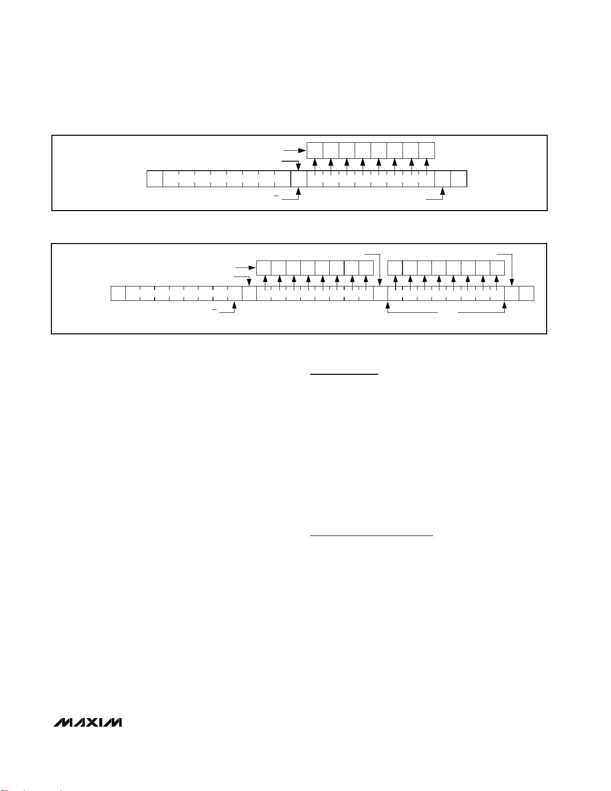
Message Format for Writing
the MAX7300
A write to the MAX7300 comprises the transmission of
the MAX7300’s slave address with the R/ W bit set to
zero, followed by at least 1 byte of information. The first
byte of information is the command byte. The command byte determines which register of the MAX7300
is to be written by the next byte, if received. If a STOP
condition is detected after the command byte is
received, then the MAX7300 takes no further action
(Figure 7) beyond storing the command byte.
Figure 1. MAX7300 Functional Diagram
P4 TO P31
AD0
AD1
SDA
SCL
CONFIGURATION
GPIO
PORT CHANGE
DETECTOR
GPIO DATA
8
ADDRESS
MATCHER
7
D0 D1 D2 D3 D4 D5 D6 D7 D8 D9 D10 D11 D12 D13 D14 D15
7
SLAVE ADDRESS BYTE
R/W
8
DATA BYTE COMMAND BYTE
TO/FROM DATA REGISTERS
R/W7-BIT DEVICE ADDRESS
PORT REGISTERS
MASK REGISTER
CONFIGURATION
REGISTERS
CED ATA
8
COMMAND
REGISTER DECODE
8
TO COMMAND REGISTERS
COMMAND BYTEDATA BYTE
R/W
Page 9

MAX7300
2-Wire-Interfaced, 2.5V to 5.5V, 20-Port or
28-Port I/O Expander
__________________________________________________________________________
Any bytes received after the command byte are considered data bytes. The first data byte goes into the internal register of the MAX7300 selected by the command
byte (Figure 8). If multiple data bytes are transmitted
before a STOP condition is detected, these bytes are
generally stored in subsequent MAX7300 internal registers because the command byte address generally
autoincrements (Table 4).
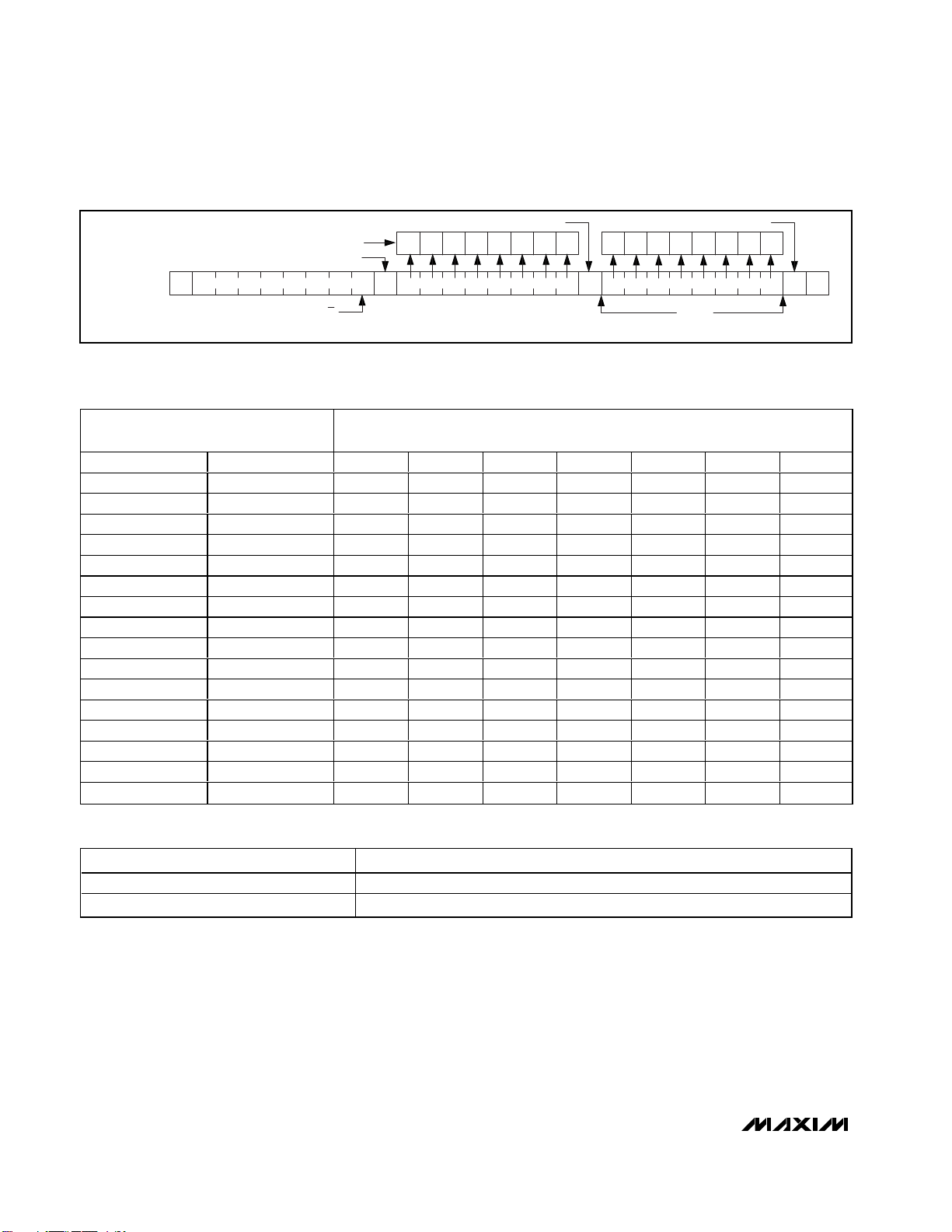
Message Format for Reading
The MAX7300 is read using the MAX7300’s internally
stored command byte as address pointer, the same way
the stored command byte is used as address pointer for
a write. The pointer generally autoincrements after each
data byte is read using the same rules as for a write
(Table 4). Thus, a read is initiated by first configuring the
MAX7300’s command byte by performing a write (Figure
7). The master can now read ‘n’ consecutive bytes from
the MAX7300, with the first data byte being read from the
register addressed by the initialized command byte
(Figure 9). When performing read-after-write verification,
remember to reset the command byte’s address
because the stored control byte address generally has
been autoincremented after the write (Table 4). Table 5
is the register address map.
Figure 2. 2-Wire Serial Interface Timing Details
Figure 3. Start and Stop Conditions
Figure 4. Bit Transfer
SDA
t
SU, DAT
t
LOW
SCL
t
t
HD, STA
START CONDITION
HIGH
t
R
t
F
SDA
SCL
S
START
CONDITION
t
HD, DAT
t
SU, STA
REPEATED START CONDITION
t
HD, STA
t
SU, STO
P
STOP
CONDITION
t
BUF
START CONDITIONSTOP CONDITION
SDA
SCL
DATA LINE STABLE; DATA VALID
CHANGE OF DATA ALLOWED
Page 10
MAX7300
2-Wire-Interfaced, 2.5V to 5.5V, 20-Port or
28-Port I/O Expander
10 ______________________________________________________________________________________
Operation with Multiple Masters
If the MAX7300 is operated on a 2-wire interface with
multiple masters, a master reading the MAX7300 should
use a repeated start between the write, which sets the
MAX7300’s address pointer, and the read(s) that takes
the data from the location(s). This is because it is possible for master 2 to take over the bus after master 1 has
set up the MAX7300’s address pointer, but before
master 1 has read the data. If master 2 subsequently
changes, the MAX7300’s address pointer, then master
1’s delayed read can be from an unexpected location.
Command Address Autoincrementing
Address autoincrementing allows the MAX7300 to be
configured with the shortest number of transmissions
by minimizing the number of times the command
address needs to be sent. The command address
stored in the MAX7300 generally increments after each
data byte is written or read (Table 4).
Initial Power-Up
On initial power-up, all control registers are reset and
the MAX7300 enters shutdown mode (Table 6).
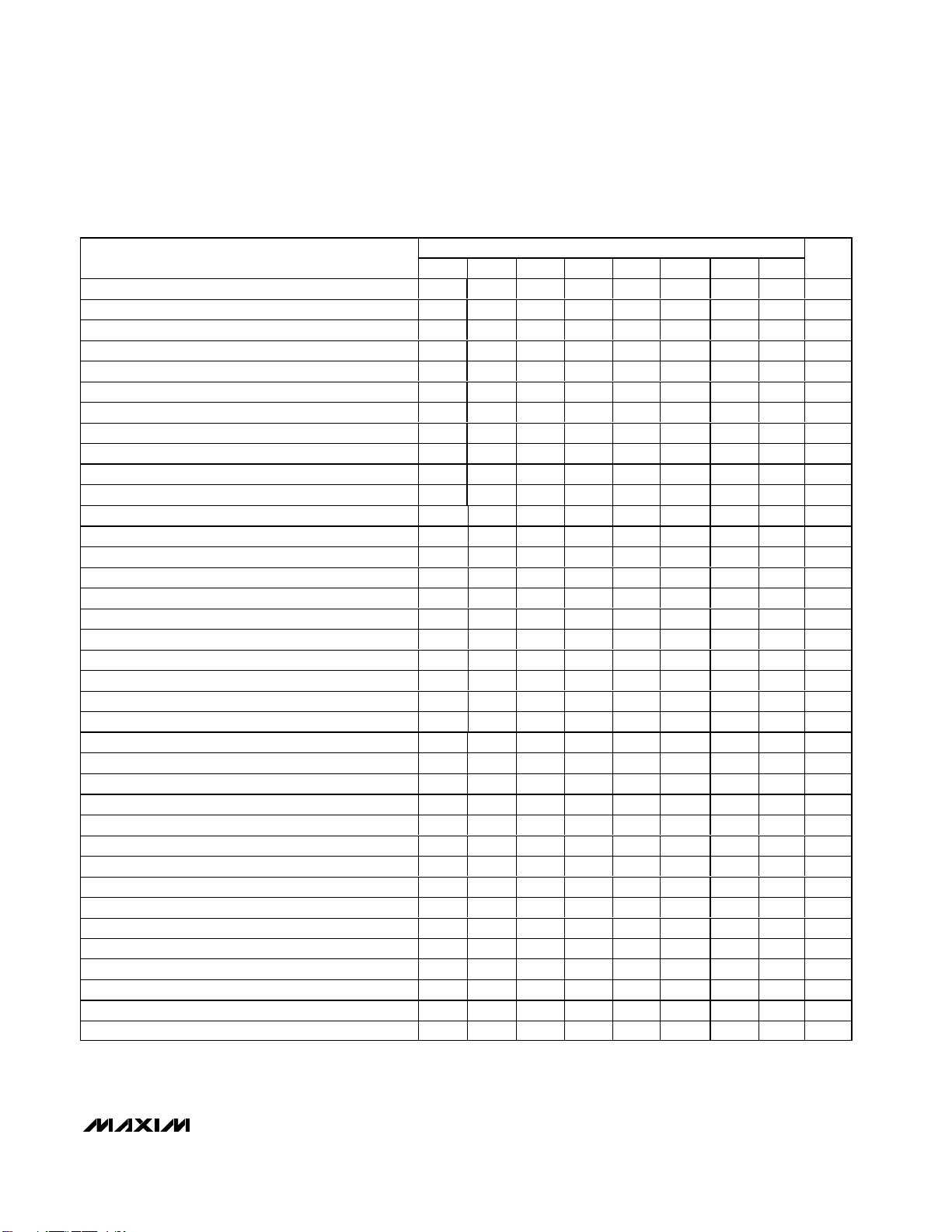
Transition (Port Data Change) Detection
Port transition detection allows seven maskable ports
P24 to P30 to be continuously monitored for changes in
their logic status (Figure 10). Enable transition detection by setting the M bit in the configuration register
(Table 9) after setting the mask register. If port 31 is
configured as an output (Tables 1 and 2), then P31
automatically becomes an interrupt request (IRQ) output to flag detected transitions. Port 31 can be configured and used as a general-purpose input port instead,
if not required for use as the IRQ output.
The mask register determines which of the seven ports
P24 to P30 are monitored (Table 10). Set the appropriate mask bit to enable that port for transition detect.
Clear the mask bit if transitions on that port are to be
ignored by the transition detection logic. Ports are monitored regardless of their I/O configuration, both input
and output.
Figure 5. Acknowledge
Figure 6. Slave Address
START CONDITION
SCL
BY TRANSMITTER
SDA
SDA
BY RECEIVER
SDA
SCL
1 0 A3 A2 A1 A00
MSB
CLOCK PULSE FOR ACKNOWLEDGMENT
12 89
S
R/W
LSB
ACK
Page 11
MAX7300
2-Wire-Interfaced, 2.5V to 5.5V, 20-Port or
28-Port I/O Expander
______________________________________________________________________________________ 11
The MAX7300 maintains an internal 7-bit snapshot register to hold the comparison copy of the logic states of
ports P24 to P30. The snapshot register is updated with
the condition of P24 to P31 whenever the configuration
register is written with the M bit set. The update action
occurs regardless of the previous state of the M bit so
that it is not necessary to clear the M bit and then reset
it in order to update the snapshot register.
When the data change detection bit is set, the MAX7300
continuously compares the snapshot register against
the changing states of P24 to P31. When a difference
occurs, the IRQ bit (mask register bit D7) is set and IRQ
port P31 goes high if it is configured as an output.
The IRQ bit and IRQ output remain set until the mask
register is next read or written, so if the IRQ is set, then
the mask register reads with bit D7 set. Writing the
mask register clears the IRQ bit and resets the IRQ output, regardless of the value of bit D7 written.
External Component R
ISET
The MAX7300 uses an external resistor, R
ISET,
to set
internal biasing. Use a resistor value of 39kΩ.
Applications Information
Low-Voltage Operation
The MAX7300 operates down to 2V supply voltage
(although the sourcing and sinking currents are not
guaranteed), providing that the MAX7300 is powered up
initially to at least 2.5V to trigger the device’s internal
reset.
Power-Supply Considerations
The MAX7300 operates with power-supply voltages of
2.5V to 5.5V. Bypass the power supply to GND with a
0.047µF capacitor as close to the device as possible.
Add a 1µF capacitor if the MAX7300 is far away from
the board’s input bulk decoupling capacitor.
Chip Information
TRANSISTOR COUNT: 33,559
PROCESS: CMOS
Figure 7. Command Byte Received
Figure 8. Command and Single Data Byte Received
COMMAND BYTE IS STORED ON RECEIPT OF STOP CONDITION
ACKNOWLEDGE FROM MAX7300
SAAP0
HOW COMMAND BYTE AND DATA BYTE MAP INTO MAX7300’s REGISTER
SAAAP0
ACKNOWLEDGE FROM MAX7300
SLAVE ADDRESS
SLAVE ADDRESS
R/W
D15 D14 D13 D12 D11 D10 D9 D8 D1 D0D3 D2D5 D4D7 D6
R/W
D15 D14 D13 D12 D11 D10 D9 D8
COMMAND BYTE
ACKNOWLEDGE FROM MAX7300
ACKNOWLEDGE FROM MAX7300 ACKNOWLEDGE FROM MAX7300
COMMAND BYTE
AUTOINCREMENT MEMORY WORD ADDRESS
DATA BYTE
1 BYTE
Page 12
MAX7300
2-Wire-Interfaced, 2.5V to 5.5V, 20-Port or
28-Port I/O Expander
12 ______________________________________________________________________________________
Figure 9. ‘n’ Data Bytes Received
Table 3. MAX7300 Address Map
Table 4. Autoincrement Rules
HOW COMMAND BYTE AND DATA BYTE MAP INTO MAX7300’s REGISTER
ACKNOWLEDGE FROM MAX7300
SA AAP0
CONNECTION
AD1 AD0 A6 A5 A4 A3 A2 A1 A0
GND GND 1 0 0 0 0 0 0
GND V+ 1000001
GND SDA 1000010
GND SCL 1000011
V+ GND 1000100
V+ V+ 1000101
V+ SDA 1000110
V+ SCL 1000111
SDA GND 1001000
SDA V+ 1001001
SDA SDA 1 0 0 1 0 1 0
SDA SCL 1 0 0 1 0 1 1
SCL GND 1001100
SCL V+ 1001101
SCL SDA 1 0 0 1 1 1 0
SCL SCL 1 0 0 1 1 1 1
SLAVE ADDRESS
PIN
R/W
ACKNOWLEDGE FROM MAX7300
D15 D14 D13 D12 D11 D10 D9 D8 D1 D0D3 D2D5 D4D7 D6
COMMAND BYTE
AUTOINCREMENT MEMORY WORD ADDRESS
DEVICE ADDRESS
ACKNOWLEDGE FROM MAX7300
DATA BYTE
‘n’ BYTES
COMMAND BYTE ADDRESS RANGE AUTOINCREMENT BEHAVIOR
x0000000 to x1111110 Command address autoincrements after byte read or written
x1111111 Command address remains at x1111111 after byte written or read
Page 13
MAX7300
2-Wire-Interfaced, 2.5V to 5.5V, 20-Port or
28-Port I/O Expander
______________________________________________________________________________________ 13
Table 5. Register Address Map
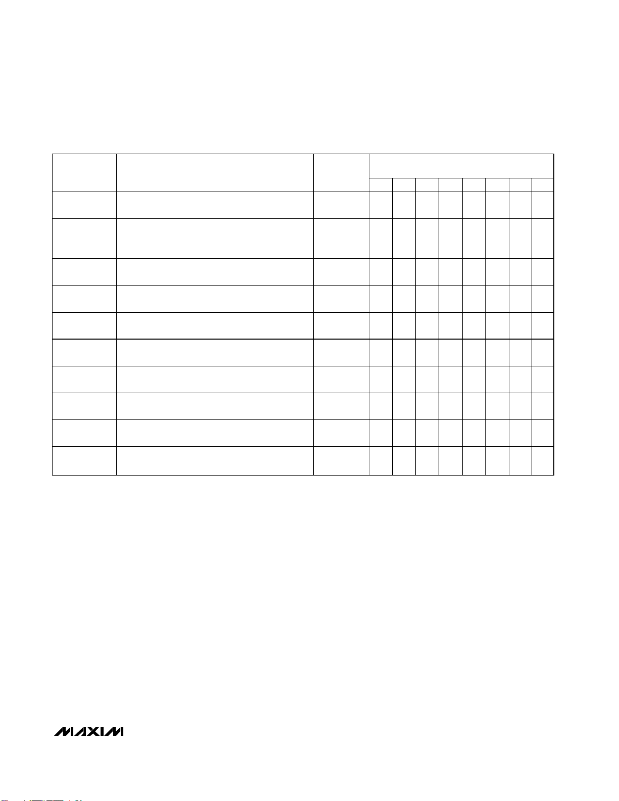
REGISTER
No-Op X 0 0 0 0 0 0 0 0x00
Configuration X 0 0 0 0 1 0 0 0x04
Transition Detect Mask X 0 0 0 0 1 1 0 0x06
Factory Reserved; do not write to this port X 0 0 0 0 1 1 1 0x07
Port Configuration P7, P6, P5, P4 X 0 0 0 1 0 0 1 0x09
Port Configuration P11, P10, P9, P8 X 0 0 0 1 0 1 0 0x0A
Port Configuration P15, P14, P13, P12 X 0 0 0 1 0 1 1 0x0B
Port Configuration P19, P18, P17, P16 X 0 0 0 1 1 0 0 0x0C
Port Configuration P23, P22, P21, P20 X 0 0 0 1 1 0 1 0x0D
Port Configuration P27, P26, P25, P24 X 0 0 0 1 1 1 0 0x0E
Port Configuration P31, P30, P29, P28 X 0 0 0 1 1 1 1 0x0F
Port 0 only (virtual port, no action) X 0 1 0 0 0 0 0 0x20
Port 1 only (virtual port, no action) X 0 1 0 0 0 0 1 0x21
Port 2 only (virtual port, no action) X 0 1 0 0 0 1 0 0x22
Port 3 only (virtual port, no action) X 0 1 0 0 0 1 1 0x23
Port 4 only X 0 1 0 0 1 0 0 0x24
Port 5 only X 0 1 0 0 1 0 1 0x25
Port 6 only X 0 1 0 0 1 1 0 0x26
Port 7 only X 0 1 0 0 1 1 1 0x27
Port 8 only X 0 1 0 1 0 0 0 0x28
Port 9 only X 0 1 0 1 0 0 1 0x29
Port 10 only X 0 1 0 1 0 1 0 0x2A
Port 11 only X 0 1 0 1 0 1 1 0x2B
Port 12 only X 0 1 0 1 1 0 0 0x2C
Port 13 only X 0 1 0 1 1 0 1 0x2D
Port 14 only X 0 1 0 1 1 1 0 0x2E
Port 15 only X 0 1 0 1 1 1 1 0x2F
Port 16 only X 0 1 1 0 0 0 0 0x30
Port 17 only X 0 1 1 0 0 0 1 0x31
Port 18 only X 0 1 1 0 0 1 0 0x32
Port 19 only X 0 1 1 0 0 1 1 0x33
Port 20 only X 0 1 1 0 1 0 0 0x34
Port 21 only X 0 1 1 0 1 0 1 0x35
Port 22 only X 0 1 1 0 1 1 0 0x36
Port 23 only X 0 1 1 0 1 1 1 0x37
Port 24 only X 0 1 1 1 0 0 0 0x38
Port 25 only X 0 1 1 1 0 0 1 0x39
D15 D14 D13 D12 D11 D10 D9 D8
COMMAND ADDRESS
HEX
CODE
Page 14

MAX7300
2-Wire-Interfaced, 2.5V to 5.5V, 20-Port or
28-Port I/O Expander
14 ______________________________________________________________________________________
Table 5. Register Address Map (continued)
Note: Unused bits read as zero.
REGISTER
Port 26 only X 0 1 1 1 0 1 0 0x3A
Port 27 only X 0 1 1 1 0 1 1 0x3B
Port 28 only X 0 1 1 1 1 0 0 0x3C
Port 29 only X 0 1 1 1 1 0 1 0x3D
Port 30 only X 0 1 1 1 1 1 0 0x3E
Port 31 only X 0 1 1 1 1 1 1 0x3F
4 ports 4–7 (data bits D0–D3) X 1 0 0 0 0 0 0 0x40
5 ports 4–8 (data bits D0–D4) X 1 0 0 0 0 0 1 0x41
6 ports 4–9 (data bits D0–D5) X 1 0 0 0 0 1 0 0x42
7 ports 4–10 (data bits D0–D6) X 1 0 0 0 0 1 1 0x43
8 ports 4–11 X 1 0 0 0 1 0 0 0x44
8 ports 5–12 X 1 0 0 0 1 0 1 0x45
8 ports 6–13 X 1 0 0 0 1 1 0 0x46
8 ports 7–14 X 1 0 0 0 1 1 1 0x47
8 ports 8–15 X 1 0 0 1 0 0 0 0x48
8 ports 9–16 X 1 0 0 1 0 0 1 0x49
8 ports 10–17 X 1 0 0 1 0 1 0 0x4A
8 ports 11–18 X 1 0 0 1 0 1 1 0x4B
8 ports 12–19 X 1 0 0 1 1 0 0 0x4C
8 ports 13–20 X 1 0 0 1 1 0 1 0x4D
8 ports 14–21 X 1 0 0 1 1 1 0 0x4E
8 ports 15–22 X 1 0 0 1 1 1 1 0x4F
8 ports 16–23 X 1 0 1 0 0 0 0 0x50
8 ports 17–24 X 1 0 1 0 0 0 1 0x51
8 ports 18–25 X 1 0 1 0 0 1 0 0x52
8 ports 19–26 X 1 0 1 0 0 1 1 0x53
8 ports 20–27 X 1 0 1 0 1 0 0 0x54
8 ports 21–28 X 1 0 1 0 1 0 1 0x55
8 ports 22–29 X 1 0 1 0 1 1 0 0x56
8 ports 23–30 X 1 0 1 0 1 1 1 0x57
8 ports 24–31 X 1 0 1 1 0 0 0 0x58
7 ports 25–31 X 1 0 1 1 0 0 1 0x59
6 ports 26–31 X 1 0 1 1 0 1 0 0x5A
5 ports 27–31 X 1 0 1 1 0 1 1 0x5B
4 ports 28–31 X 1 0 1 1 1 0 0 0x5C
3 ports 29–31 X 1 0 1 1 1 0 1 0x5D
2 ports 30–31 X 1 0 1 1 1 1 0 0x5E
1 port 31 only X 1 0 1 1 1 1 1 0x5F
D15 D14 D13 D12 D11 D10 D9 D8
COMMAND ADDRESS
HEX
CODE
Page 15
MAX7300
2-Wire-Interfaced, 2.5V to 5.5V, 20-Port or
28-Port I/O Expander
______________________________________________________________________________________ 15
Table 6. Power-Up Configuration
X = unused bits; if read, zero results.
REGISTER
FUNCTION
Port Register
Bits 4 to 31
Configuration
Register
Input Mask
Register
Port
Configuration
Port
Configuration
Port
Configuration
Port
Configuration
Port
Configuration
Port
Configuration
Port
Configuration
P7, P6, P5, P4: GPIO Inputs without Pullup 0x09 1 0 1 0 1 0 1 0
P11, P10, P9, P8: GPIO Inputs without Pullup 0x0A 1 0 1 0 1 0 1 0
P15, P14, P13, P12: GPIO Inputs without Pullup 0x0B 1 0 1 0 1 0 1 0
P19, P18, P17, P16: GPIO Inputs without Pullup 0x0C 1 0 1 0 1 0 1 0
P23, P22, P21, P20: GPIO Inputs without Pullup 0x0D 1 0 1 0 1 0 1 0
P27, P26, P25, P24: GPIO Inputs without Pullup 0x0E 1 0 1 0 1 0 1 0
P31, P30, P29, P28: GPIO Inputs without Pullup 0x0F 1 0 1 0 1 0 1 0
POWER-UP CONDITION
GPIO Output Low
Shutdown Enabled
Transition Detection Disabled
All Clear (Masked Off) 0x06 X 0 0 0 0 0 0 0
ADDRESS
CODE
(HEX)
0x24 to
0x3F
0x04 0 0 X X X X X 0
D7 D6 D5 D4 D3 D2 D1 D0
XXXXXXX0
REGISTER DATA
Page 16

MAX7300
2-Wire-Interfaced, 2.5V to 5.5V, 20-Port or
28-Port I/O Expander
16 ______________________________________________________________________________________
Table 7. Configuration Register Format
Table 8. Shutdown Control (S Data Bit D0) Format
Table 9. Transition Detection Control (M Data Bit D7) Format
Table 10. Transition Detection Mask Register
*IRQ is automatically cleared after it is read.
FUNCTION
Configuration Register 0x04 M 0 XXXXXS
FUNCTION
Shutdown 0x04 M 0 XXXXX0
Normal Operation 0x04 M 0 XXXXX1
FUNCTION
Disabled 0x04 0 0 XXXXXS
Enabled 0x04 1 0 XXXXXS
FUNCTION
REGISTER
ADDRESS
(HEX)
ADDRESS CODE
(HEX)
ADDRESS CODE
(HEX)
ADDRESS CODE
(HEX)
READ/
WRITE
D7 D6 D5 D4 D3 D2 D1 D0
D7 D6 D5 D4 D3 D2 D1 D0
D7 D6 D5 D4 D3 D2 D1 D0
D7 D6 D5 D4 D3 D2 D1 D0
REGISTER DATA
REGISTER DATA
REGISTER DATA
REGISTER DATA
Mask
Register
0x06
Read IRQ Status*
Write Unchanged
Port
30
mask
Port
29
mask
Port
28
mask
Port
27
mask
Port
26
mask
Port
25
mask
Port
24
mask
Page 17

MAX7300
2-Wire-Interfaced, 2.5V to 5.5V, 20-Port or
28-Port I/O Expander
______________________________________________________________________________________ 17
Figure 10. Maskable GPIO Ports P24 to P31
P30
P29
P28
P27
P31
GPIO INPUT
CONDITIONING
OUTPUT LATCH
OUTPUT LATCH
CONFIGURATION REGISTER M BIT = 1
GPIO INPUT
CONDITIONING
GPIO/PORT OUTPUT LATCH
GPIO INPUT
CONDITIONING
GPIO/PORT OUTPUT LATCH
GPIO INPUT
CONDITIONING
GPIO/PORT OUTPUT LATCH
GPIO INPUT
CONDITIONING
GPIO/PORT OUTPUT LATCH
GPIO/PORT
IRQ
GPIO/PORT OUT
GPIO/PORT OUT
GPIO/PORT OUT
GPIO/PORT OUT
GPIO IN
GPIO IN
GPIO IN
GPIO IN
GPIO IN
GPIO/PORT OUT
IRQ STATUS STORED AS MSB OF MASK REGISTER
R
S
CLOCK PULSE AFTER EACH READ ACCESS TO MASK REGISTER
D Q
MASK REGISTER BIT 6
D Q
MASK REGISTER BIT 5
D Q
MASK REGISTER BIT 4
D Q
MASK REGISTER BIT 3
OR
GPIO INPUT
P26
P25
P24
CONDITIONING
GPIO/PORT OUTPUT LATCH
GPIO INPUT
CONDITIONING
GPIO/PORT OUTPUT LATCH
GPIO INPUT
CONDITIONING
GPIO/PORT OUTPUT LATCH
GPIO IN
GPIO/PORT OUT
GPIO IN
GPIO/PORT OUT
GPIO IN
GPIO/PORT OUT
D Q
MASK REGISTER BIT 2
D Q
MASK REGISTER BIT 1
D Q
MASK REGISTER LSB
CLOCK PULSE WHEN WRITING CONFIGURATION REGISTER WITH M BIT SET
Page 18

MAX7300
2-Wire-Interfaced, 2.5V to 5.5V, 20-Port or
28-Port I/O Expander
18 ______________________________________________________________________________________
Pin Configurations (continued)
TOP VIEW
GND
GND
GND
ISET
1
GND
2
GND
3
AD0
4
P8
5
P12
6
7
P9
P13
8
P10
9
10
P14
P11
11
P15
12
13
P16
P17
14
15
P18
16
P19
17
P20
18 P22
P21
MAX7300
MAX7300
P20
P19
ISETV+AD1
P21
QFN
AD0
V+
36
AD1
35
SCL
34
33
SDA
32
P4
31
P31
P5
30
P30
29
P6
28
P29
27
P7
26
P28
25
P27
24
P26
23
22
P25
21
P24
20
P23
19
P8
P12
P9
P13
P10
P14
P11
P15
P16
P17
403938373635343332
1
2
3
4
5
6
7
8
9
10
111213141516171819
P18
N.C.
P22
P23
SCL
P24
SDA
P25
N.C.
31
20
N.C.
30
P4
29
P31
28
P5
27
P30
P6
26
P29
25
P7
24
P28
23
P27
22
P26
21
SSOP
Page 19

MAX7300
2-Wire-Interfaced, 2.5V to 5.5V, 20-Port or
28-Port I/O Expander
______________________________________________________________________________________ 19
MAX7300
Package Information
(The package drawing(s) in this data sheet may not reflect the most current specifications. For the latest package outline information,
go to www.maxim-ic.com/packages.)
12
MAX
0.078
0.008
0.015
0.008
0.212
0.311
0.037
8∞
MILLIMETERS
MIN
1.73 1.99
0.05
0.25
0.09
5.20
7.65
0.63
INCHES
DIM
MIN
A
0.068
A1
0.002
B
0.010
C
HE
N
A
e
D
B
A1
D
E
e
H
L
0.004
SEE VARIATIONS
0.205
0.0256 BSC
0.301
0.025
0∞
L
NOTES:
1. D&E DO NOT INCLUDE MOLD FLASH.
2. MOLD FLASH OR PROTRUSIONS NOT TO EXCEED .15 MM (.006").
3. CONTROLLING DIMENSION: MILLIMETERS.
4. MEETS JEDEC MO150.
5. LEADS TO BE COPLANAR WITHIN 0.10 MM.
0.38
0.20
5.38
0.65 BSC
0.95
0∞
MAX
0.21
7.90
8∞
PROPRIETARY INFORMATION
TITLE:
INCHES
MIN
D
0.239
D
0.239
D
0.278
D
0.317
0.397
D
MILLIMETERS
MAX
0.249
0.249
0.289
0.328
0.407
PACKAGE OUTLINE, SSOP, 5.3 MM
21-0056
MIN
6.07
6.07
7.07
8.07
10.07
MAX
6.33
6.33
7.33
8.33
10.33
SSOP.EPS
N
14L
16L
20L
24L
28L
C
REV.DOCUMENT CONTROL NO.APPROVAL
1
C
1
Page 20

MAX7300
2-Wire-Interfaced, 2.5V to 5.5V, 20-Port or
28-Port I/O Expander
20 ______________________________________________________________________________________
Package Information (continued)
(The package drawing(s) in this data sheet may not reflect the most current specifications. For the latest package outline information,
go to www.maxim-ic.com/packages.)
36L,40L, QFN.EPS
Page 21

MAX7300
2-Wire-Interfaced, 2.5V to 5.5V, 20-Port or
28-Port I/O Expander
______________________________________________________________________________________ 21
Package Information (continued)
(The package drawing(s) in this data sheet may not reflect the most current specifications. For the latest package outline information,
go to www.maxim-ic.com/packages.)
U
Page 22

MAX7300
2-Wire-Interfaced, 2.5V to 5.5V, 20-Port or
28-Port I/O Expander
Maxim cannot assume responsibility for use of any circuitry other than circuitry entirely embodied in a Maxim product. No circuit patent licenses are
implied. Maxim reserves the right to change the circuitry and specifications without notice at any time.
22 ____________________Maxim Integrated Products, 120 San Gabriel Drive, Sunnyvale, CA 94086 408-737-7600
© 2003 Maxim Integrated Products Printed USA is a registered trademark of Maxim Integrated Products.
Package Information (continued)
(The package drawing(s) in this data sheet may not reflect the most current specifications. For the latest package outline information,
go to www.maxim-ic.com/packages.)
e
36
1
TOP VIEW
FRONT VIEW
INCHES
MIN
DIM
0.096A
0.004
A1
0.012
B
0.009
C
HE
D
A1
A
B
C
e 0.0315 BSC 0.80 BSC
0.291
E
H 0.4140.398 10.11 10.51
0.020L
D 0.6120.598
L
MAX
0.104
0.011
0.017
0.013
0.299
0.040
MILLIMETERS
MAX
MIN
2.65
2.44
0.29
0.10
0.44
0.30
0.23
0.32
7.40 7.60
0.51 1.02
15.20 15.55
0∞-8∞
SSOP.EPS
SIDE VIEW
PROPRIETARY INFORMATION
TITLE:
PACKAGE OUTLINE, 36L SSOP, 0.80 MM PITCH
21-0040 E
REV.DOCUMENT CONTROL NO.APPROVAL
1
1
 Loading...