Maxim MAX7219ENG, MAX7219ERG, MAX7219EWG, MAX7219C-D, MAX7219CNG Datasheet
...
_______________General Description
The MAX7219/MAX7221 are compact, serial input/output common-cathode display drivers that interface
microprocessors (µPs) to 7-segment numeric LED displays of up to 8 digits, bar-graph displays, or 64 individual LEDs. Included on-chip are a BCD code-B
decoder, multiplex scan circuitry, segment and digit
drivers, and an 8x8 static RAM that stores each digit.
Only one external resistor is required to set the segment current for all LEDs. The MAX7221 is compatible
with SPI™, QSPI™, and Microwire™, and has slew-ratelimited segment drivers to reduce EMI.
A convenient 3-wire serial interface connects to all
common µPs. Individual digits may be addressed and
updated without rewriting the entire display. The
MAX7219/MAX7221 also allow the user to select codeB decoding or no-decode for each digit.
The devices include a 150µA low-power shutdown
mode, analog and digital brightness control, a scanlimit register that allows the user to display from 1 to 8
digits, and a test mode that forces all LEDs on.
________________________Applications
Bar-Graph Displays
7-Segment Displays
Industrial Controllers
Panel Meters
LED Matrix Displays
____________________________Features
♦ 10MHz Serial Interface
♦ Individual LED Segment Control
♦ Decode/No-Decode Digit Selection
♦ 150µA Low-Power Shutdown (Data Retained)
♦ Digital and Analog Brightness Control
♦ Display Blanked on Power-Up
♦ Drive Common-Cathode LED Display
♦ Slew-Rate Limited Segment Drivers
for Lower EMI (MAX7221)
♦ SPI, QSPI, Microwire Serial Interface (MAX7221)
♦ 24-Pin DIP and SO Packages
MAX7219/MAX7221
Serially Interfaced, 8-Digit LED Display Drivers
________________________________________________________________
Maxim Integrated Products
1
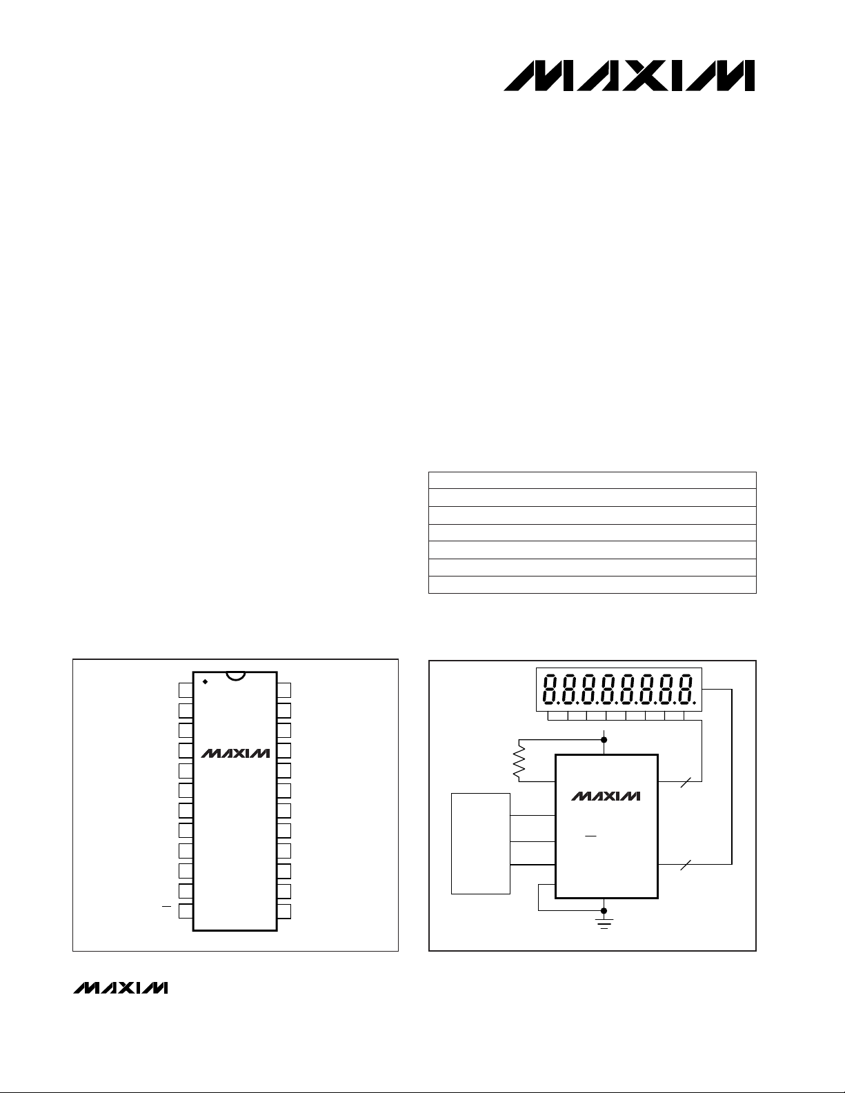
( ) MAX7221 ONLY
8-DIGIT µP DISPLAY
DIG 0–DIG 7
MOSI
I/O
SCK
18
1
12
13
9
4
DIN
µP
I
SET
9.53k
8 DIGITS
8 SEGMENTS
+5V
19
SEG A–G,
SEG DP
CLK
LOAD (CS)
GND
V+
GND
MAX7219
MAX7221
________Typical Application Circuit__________________Pin Configuration
24
23
22
21
20
19
18
17
1
2
3
4
5
6
7
8
DOUT
SEG D
SEG DP
SEG EGND
DIG 4
DIG 0
DIN
TOP VIEW
SEG C
V+
ISET
SEG GDIG 7
DIG 3
DIG 2
DIG 6
16
15
14
13
9
10
11
12
SEG B
SEG F
SEG A
CLK
( ) MAX7221 ONLY
LOAD (CS)
DIG 1
DIG 5
GND
DIP/SO
MAX7219
MAX7221
19-4452; Rev 3; 7/97
PART
MAX7219CNG
MAX7219CWG
MAX7219C/D 0°C to +70°C
0°C to +70°C
0°C to +70°C
TEMP. RANGE PIN-PACKAGE
24 Narrow Plastic DIP
24 Wide SO
Dice*
______________Ordering Information
Ordering Information continued at end of data sheet.
*Dice are specified at TA = +25°C.
MAX7219ENG
MAX7219EWG
MAX7219ERG -40°C to +85°C
-40°C to +85°C
-40°C to +85°C 24 Narrow Plastic DIP
24 Wide SO
24 Narrow CERDIP
SPI and QSPI are trademarks of Motorola Inc. Microwire is a trademark of National Semiconductor Corp.
For free samples & the latest literature: http://www.maxim-ic.com, or phone 1-800-998-8800.
For small orders, phone 408-737-7600 ext. 3468.
MAX7219/MAX7221
Serially Interfaced, 8-Digit LED Display Drivers
2 _______________________________________________________________________________________
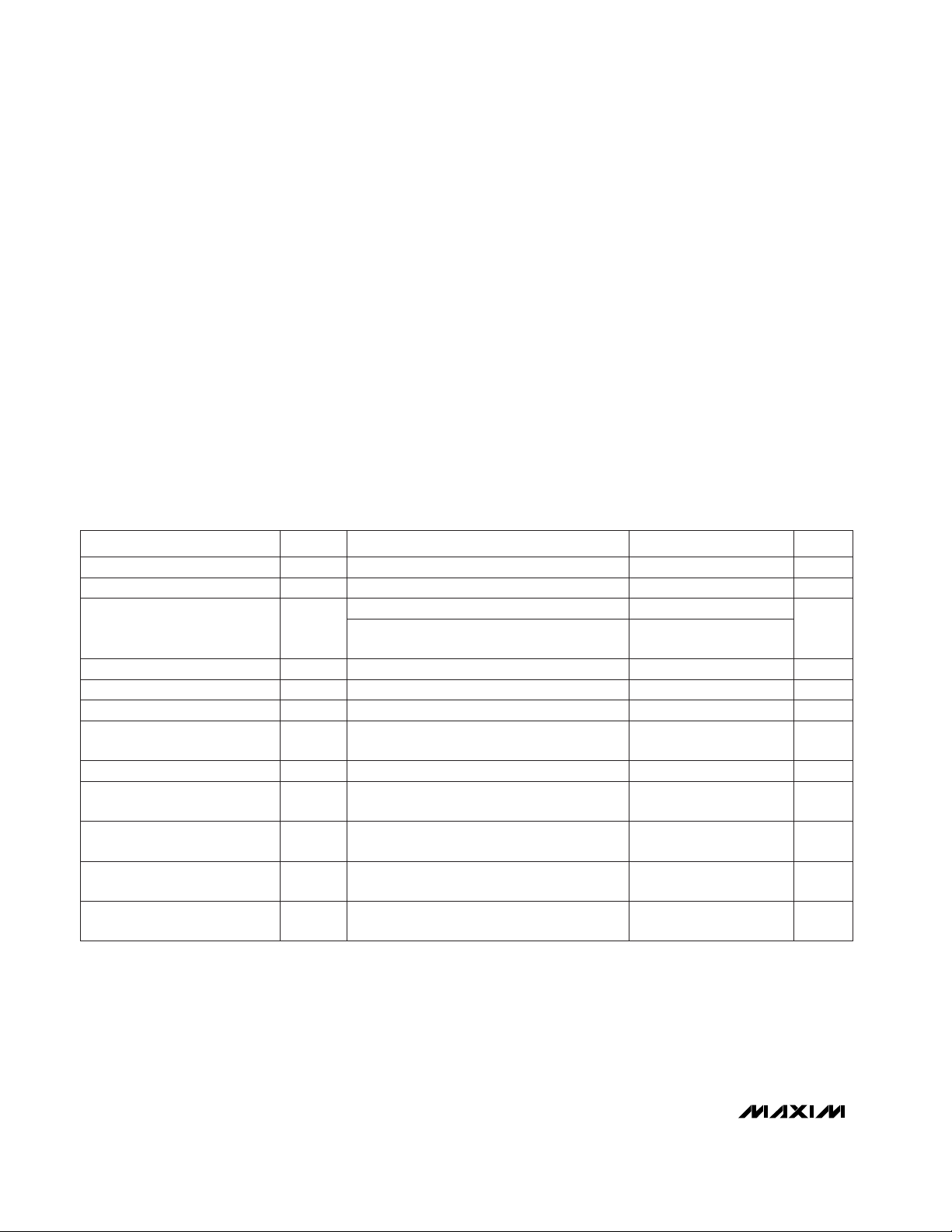
ABSOLUTE MAXIMUM RATINGS
ELECTRICAL CHARACTERISTICS
(V+ = 5V ±10%, R
SET
= 9.53kΩ ±1%, TA= T
MIN
to T
MAX
, unless otherwise noted.)
Stresses beyond those listed under “Absolute Maximum Ratings” may cause permanent damage to the device. These are stress ratings only, and functional
operation of the device at these or any other conditions beyond those indicated in the operational sections of the specifications is not implied. Exposure to
absolute maximum rating conditions for extended periods may affect device reliability.
Voltage (with respect to GND)
V+ ............................................................................-0.3V to 6V
DIN, CLK, LOAD,
CS ...............................................-0.3V to 6V
All Other Pins.............................................-0.3V to (V+ + 0.3V)
Current
DIG0–DIG7 Sink Current................................................500mA
SEGA–G, DP Source Current.........................................100mA
Continuous Power Dissipation (T
A
= +85°C)
Narrow Plastic DIP ..........................................................0.87W
Wide SO..........................................................................0.76W
Narrow CERDIP.................................................................1.1W
Operating Temperature Ranges
MAX7219C_G/MAX7221C_G ..............................0°C to +70°C
MAX7219E_G/MAX7221E_G............................-40°C to +85°C
Storage Temperature Range.............................-65°C to +160°C
Lead Temperature (soldering, 10sec).............................+300°C
R
SET
= open circuit
All digital inputs at V+ or GND, TA= +25°C
Digit off, V
DIGIT
= V+
TA= +25°C, V+ = 5V, V
OUT
= (V+ - 1V)
All segments and decimal point on,
I
SEG_
= -40mA
8 digits scanned
V+ = 5V, V
OUT
= 0.65V
TA= +25°C, V+ = 5V, V
OUT
= (V+ - 1V)
CONDITIONS
8
Operating Supply Current
µA150I+
V4.0 5.5V+Operating Supply Voltage
Shutdown Supply Current
µA-10I
DIGIT
Digit Drive Leakage
(MAX7221 only)
%3.0∆I
SEG
Segment Drive Current Matching
mA/µs10 20 50∆I
SEG
/∆t
Segment Current Slew Rate
(MAX7221 only)
mA
330
I+
Hz500 800 1300f
OSC
Display Scan Rate
mA320I
DIGIT
Digit Drive Sink Current
mA-30 -40 -45I
SEG
Segment Drive Source Current
UNITSMIN TYP MAXSYMBOLPARAMETER
Segment off, V
SEG
= 0V µA1I
SEG
Segment Drive Leakage
(MAX7221 only)
Digit off, V
DIGIT
= (V+ - 0.3V) mA-2I
DIGIT
Digit Drive Source Current
(MAX7219 only)
Segment off, V
SEG
= 0.3V mA5I
SEG
Segment Drive Sink Current
(MAX7219 only)
MAX7219/MAX7221
Serially Interfaced, 8-Digit LED Display Drivers
_______________________________________________________________________________________ 3
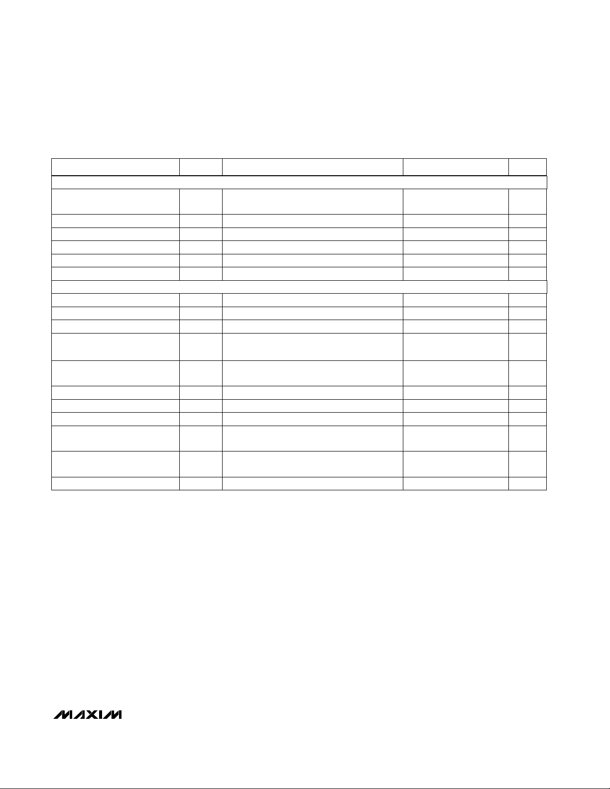
ELECTRICAL CHARACTERISTICS (continued)
(V+ = 5V ±10%, R
SET
=9.53kΩ ±1%, TA= T
MIN
to T
MAX
, unless otherwise noted.)
VIN= 0V or V+
DOUT, I
SINK
= 1.6mA
DOUT, I
SOURCE
= -1mA
CONDITIONS
µA-1 1IIH, I
IL
Input Current DIN, CLK,
LOAD, CS
V0.4V
OL
Output Low Voltage
V3.5V
IH
Logic High Input Voltage
V0.8V
IL
Logic Low Input Voltage
VV+ - 1V
OH
Output High Voltage
UNITSMIN TYP MAXSYMBOLPARAMETER
DIN, CLK, LOAD, CS
V1∆V
I
Hysteresis Voltage
ns25t
CSS
CS Fall to SCLK Rise Setup Time
(MAX7221 only)
ns100t
CP
CLK Clock Period
ns50t
CH
CLK Pulse Width High
ns50t
CL
CLK Pulse Width Low
C
LOAD
= 50pF
ns25t
DS
DIN Setup Time
ns50t
CSW
Minimum CS or LOAD Pulse
High
ns0t
DH
DIN Hold Time
ns25t
DO
Output Data Propagation Delay
ns50t
LDCK
Load-Rising Edge to Next Clock
Rising Edge (MAX7219 only)
ns0t
CSH
CLK Rise to CS or LOAD Rise
Hold Time
ms2.25t
DSPD
Data-to-Segment Delay
LOGIC INPUTS
TIMING CHARACTERISTICS
MAX7219/MAX7221
Serially Interfaced, 8-Digit LED Display Drivers
4 _______________________________________________________________________________________
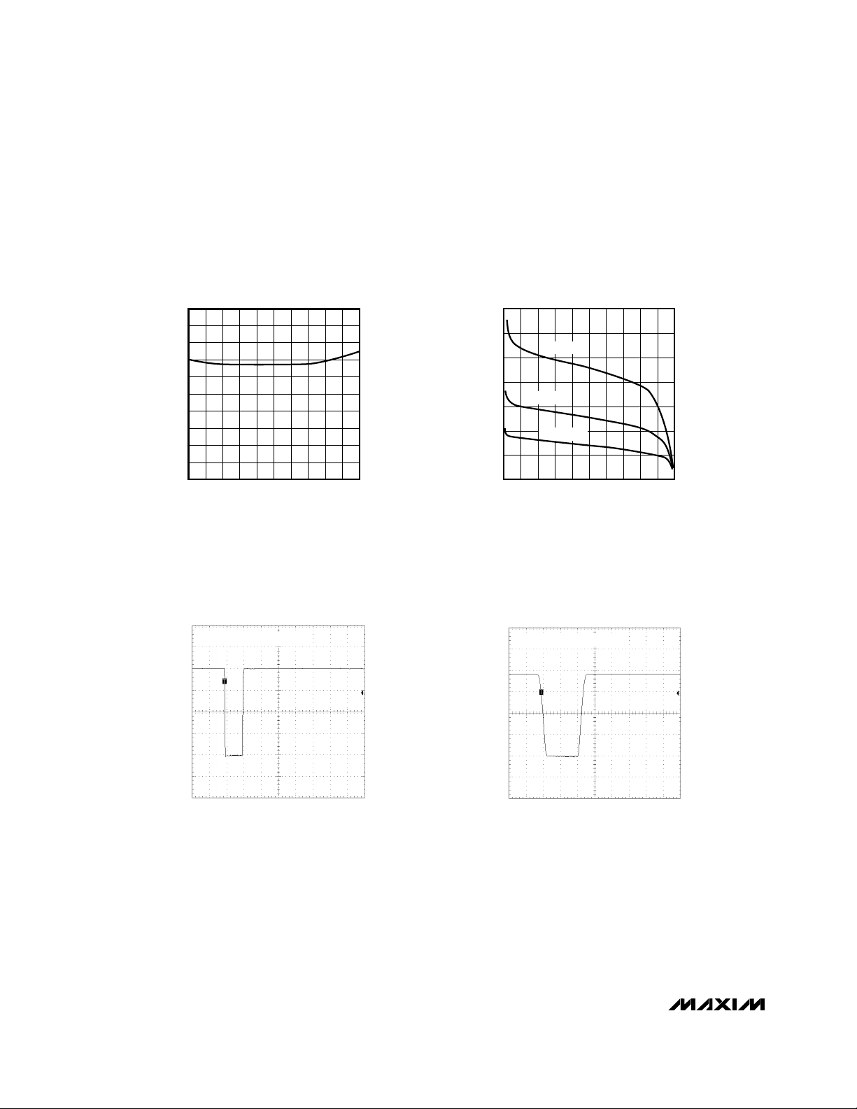
__________________________________________Typical Operating Characteristics
(V+ = +5V, TA = +25°C, unless otherwise noted.)
730
750
740
770
760
790
780
800
820
810
830
4.0 4.4 4.8 5.2 5.6 6.0
SCAN FREQUENCY vs.
POSITIVE SUPPLY VOLTAGE
MAX7219/21 01
POSITIVE SUPPLY VOLTAGE (V)
SCAN FREQUENCY (Hz)
0
20
10
40
30
60
50
70
0 1 2 3 4 5
SEGMENT DRIVER OUTPUT CURRENT
vs. OUTPUT VOLTAGE
MAX7219/21 02
OUTPUT VOLTAGE (V)
OUTPUT CURRENT (mA)
R
SET
= 10kΩ
R
SET
= 20kΩ
R
SET
= 40kΩ
MAX7219
SEGMENT OUTPUT CURRENT
MAX7219/21 03
5µs/div
10mA/div
0
MAXIMUM INTENSITY = 31/32
MAX7221
SEGMENT OUTPUT CURRENT
MAX7219/21 04
5µs/div
10mA/div
0
MAXIMUM INTENSITY = 15/16
MAX7219/MAX7221
Serially Interfaced, 8-Digit LED Display Drivers
_______________________________________________________________________________________ 5
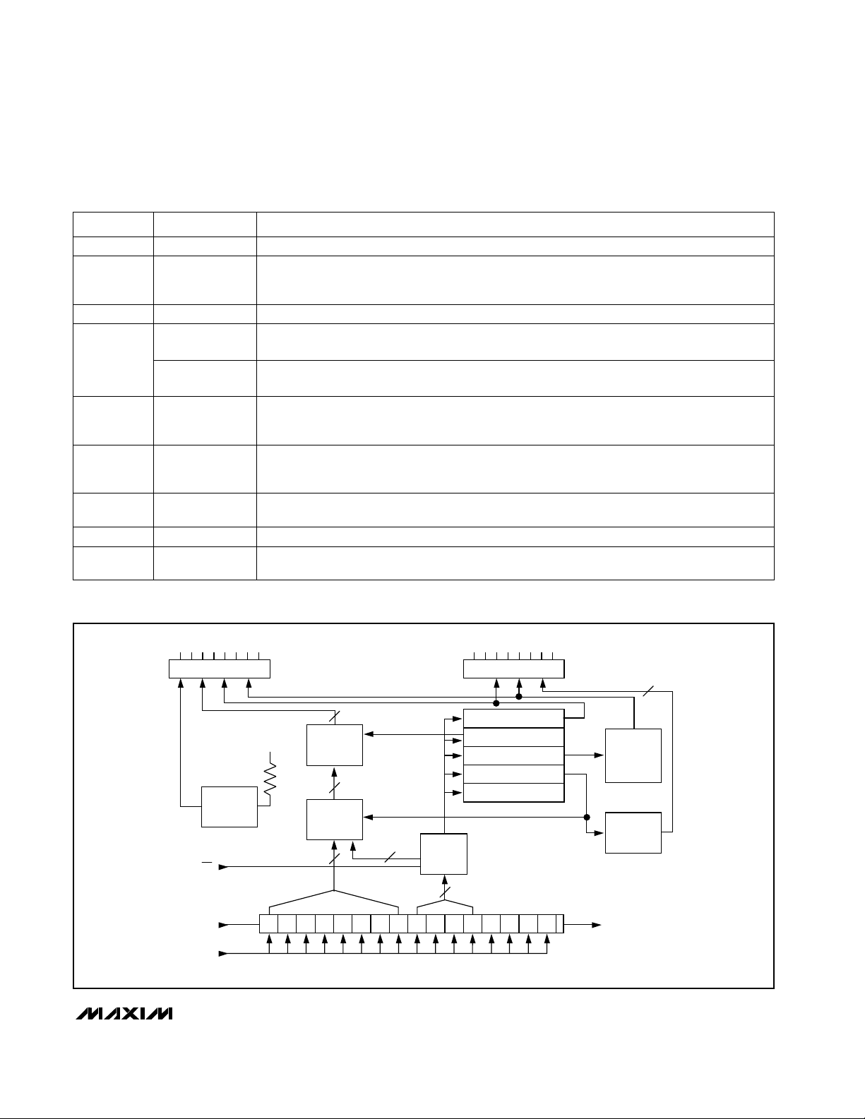
______________________________________________________________Pin Description
_________________________________________________________Functional Diagram
NAME FUNCTION
1 DIN Serial-Data Input. Data is loaded into the internal 16-bit shift register on CLK’s rising edge.
2, 3, 5–8,
10, 11
DIG 0–DIG 7
Eight-Digit Drive Lines that sink current from the display common cathode. The MAX7219 pulls
the digit outputs to V+ when turned off. The MAX7221’s digit drivers are high-impedance when
turned off.
PIN
4, 9 GND Ground (both GND pins must be connected)
12
LOAD
(MAX7219)
18 ISET
Connect to VDDthrough a resistor (R
SET
) to set the peak segment current (Refer to
Selecting
R
SET
Resistor
section).
14–17,
20–23
SEG A–SEG G,
DP
13 CLK
CS
(MAX7221)
24 DOUT
Serial-Data Output. The data into DIN is valid at DOUT 16.5 clock cycles later. This pin is used
to daisy-chain several MAX7219/MAX7221’s and is never high-impedance.
19 V+ Positive Supply Voltage. Connect to +5V.
Load-Data Input. The last 16 bits of serial data are latched on LOAD’s rising edge.
Chip-Select Input. Serial data is loaded into the shift register while CS is low. The last 16 bits of
serial data are latched on CS’s rising edge.
Serial-Clock Input. 10MHz maximum rate. On CLK’s rising edge, data is shifted into the internal shift register. On CLK’s falling edge, data is clocked out of DOUT. On the MAX7221, the
CLK input is active only while CS is low.
Seven Segment Drives and Decimal Point Drive that source current to the display. On the
MAX7219, when a segment driver is turned off it is pulled to GND. The MAX7221 segment drivers are high-impedance when turned off.
SEG A–SEG G, DP
SEGMENT DRIVERS
8
CODE B
ROM WITH
BYPASS
R
SET
D1 D2 D3 D4 D5 D6 D7 D8 D9 D10 D11 D12
8
8x8
DUAL-PORT
SRAM
8
ADDRESS
8
REGISTER
DECODER
LOAD (CS)
CLK
( ) MAX7221 ONLY
V+
SEGMENT
CURRENT
REFERENCE
DIN DOUT
D0
DIG 0–DIG 7
DIGIT DRIVERS
SHUTDOWN REGISTER
MODE REGISTER
INTENSITY REGISTER
SCAN-LIMIT REGISTER
DISPLAY-TEST REGISTER
4
D13 D14 D15
8
INTENSITY
PULSE-
WIDTH
MODULATOR
MULTIPLEX
SCAN
CIRCUITRY
(MSB)(LSB)
 Loading...