

Page 1
现货库存、技术资料、百科信息、热点资讯,精彩尽在鼎好!
General Description
The MAX7219/MAX7221 are compact, serial input/output common-cathode display drivers that interface
microprocessors (µPs) to 7-segment numeric LED displays of up to 8 digits, bar-graph displays, or 64 individual LEDs. Included on-chip are a BCD code-B
decoder, multiplex scan circuitry, segment and digit
drivers, and an 8x8 static RAM that stores each digit.
Only one external resistor is required to set the segment current for all LEDs. The MAX7221 is compatible
with SPI™, QSPI™, and MICROWIRE™, and has slewrate-limited segment drivers to reduce EMI.
A convenient 4-wire serial interface connects to all
common µPs. Individual digits may be addressed and
updated without rewriting the entire display. The
MAX7219/MAX7221 also allow the user to select codeB decoding or no-decode for each digit.
The devices include a 150µA low-power shutdown
mode, analog and digital brightness control, a scanlimit register that allows the user to display from 1 to 8
digits, and a test mode that forces all LEDs on.
For applications requiring 3V operation or segment
blinking, refer to the MAX6951 data sheet.
Applications
Features
♦ 10MHz Serial Interface
♦ Individual LED Segment Control
♦ Decode/No-Decode Digit Selection
♦ 150µA Low-Power Shutdown (Data Retained)
♦ Digital and Analog Brightness Control
♦ Display Blanked on Power-Up
♦ Drive Common-Cathode LED Display
♦ Slew-Rate Limited Segment Drivers
for Lower EMI (MAX7221)
♦ SPI, QSPI, MICROWIRE Serial Interface (MAX7221)
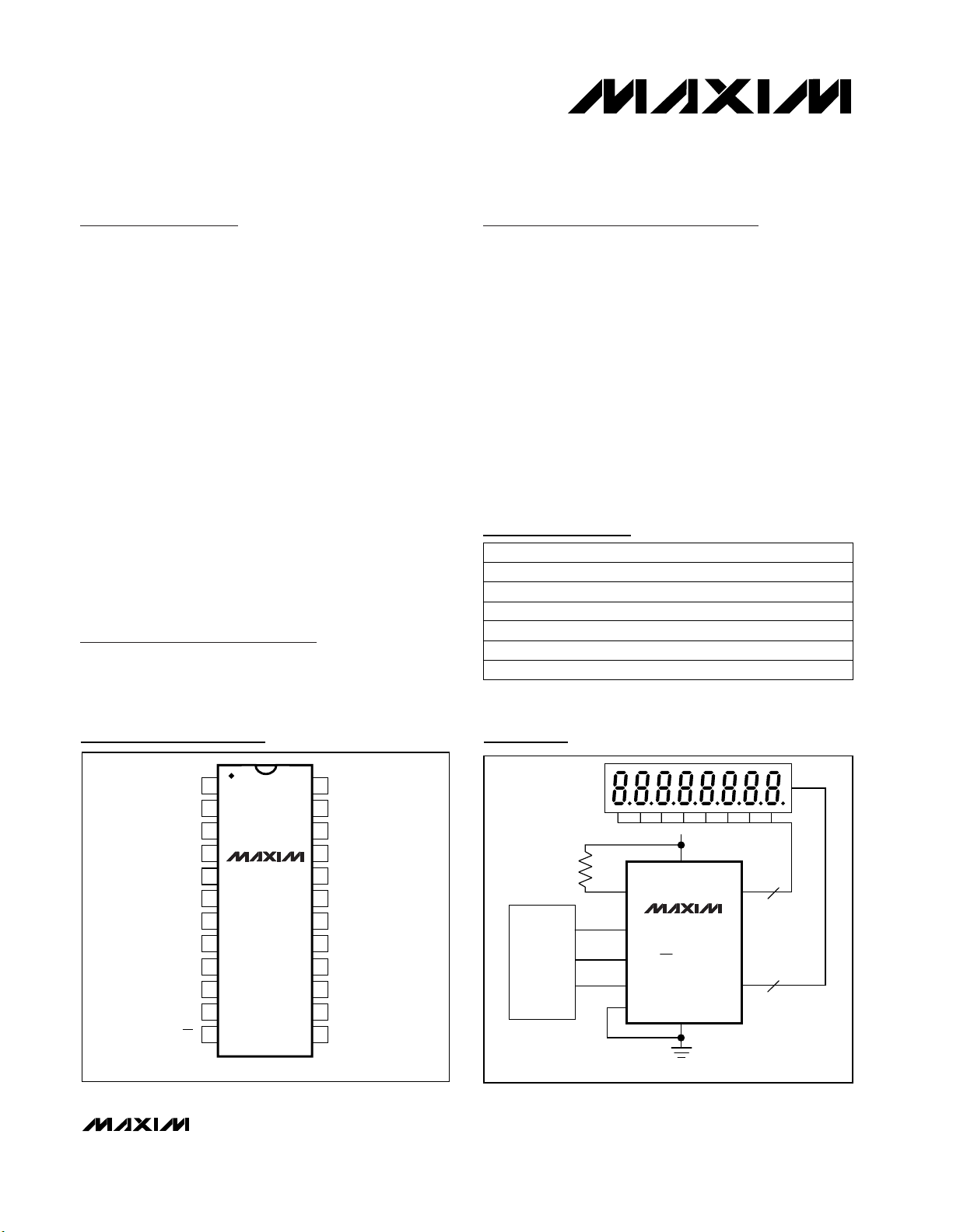
♦ 24-Pin DIP and SO Packages
MAX7219/MAX7221
Serially Interfaced, 8-Digit LED Display Drivers
________________________________________________________________ Maxim Integrated Products 1
Typical Application Circuit
Pin Configuration
24
23
22
21
20
19
18
17
1
2
3
4
5
6
7
8
DOUT
SEG D
SEG DP
SEG EGND
DIG 4
DIG 0
DIN
TOP VIEW
SEG C
V+
ISET
SEG GDIG 7
DIG 3
DIG 2
DIG 6
16
15
14
13
9
10
11
12
SEG B
SEG F
SEG A
CLK
( ) MAX7221 ONLY
LOAD (CS)
DIG 1
DIG 5
GND
DIP/SO
MAX7219
MAX7221
19-4452; Rev 4; 7/03
PART
MAX7219CNG
MAX7219CWG
MAX7219C/D 0°C to +70°C
0°C to +70°C
0°C to +70°C
TEMP RANGE PIN-PACKAGE
24 Narrow Plastic DIP
24 Wide SO
Dice*
Ordering Information
Ordering Information continued at end of data sheet.
*Dice are specified at T
A
= +25°C.
MAX7219ENG
MAX7219EWG
MAX7219ERG -40°C to +85°C
-40°C to +85°C
-40°C to +85°C 24 Narrow Plastic DIP
24 Wide SO
24 Narrow CERDIP
SPI and QSPI are trademarks of Motorola Inc. MICROWIRE is a trademark of National Semiconductor Corp.
Bar-Graph Displays
Industrial Controllers
Panel Meters
LED Matrix Displays
For pricing, delivery, and ordering information, please contact Maxim/Dallas Direct! at
1-888-629-4642, or visit Maxim’s website at www.maxim-ic.com.
( ) MAX7221 ONLY
+5V
9.53k
18
I
SET
MOSI
µP
I/O
SCK
1
DIN
12
LOAD (CS)
13
CLK
9
GND
8-DIGIT µP DISPLAY
19
V+
DIG 0–DIG 7
MAX7219
MAX7221
GND
4
SEG A–G,
SEG DP
8 DIGITS
8 SEGMENTS
Page 2
MAX7219/MAX7221
Serially Interfaced, 8-Digit LED Display Drivers
2 _______________________________________________________________________________________
ABSOLUTE MAXIMUM RATINGS
ELECTRICAL CHARACTERISTICS
(V+ = 5V ±10%, R
SET
= 9.53kΩ ±1%, TA= T
MIN
to T
MAX
, unless otherwise noted.)
Stresses beyond those listed under “Absolute Maximum Ratings” may cause permanent damage to the device. These are stress ratings only, and functional
operation of the device at these or any other conditions beyond those indicated in the operational sections of the specifications is not implied. Exposure to
absolute maximum rating conditions for extended periods may affect device reliability.
Voltage (with respect to GND)
V+ ............................................................................-0.3V to 6V
DIN, CLK, LOAD, CS ...............................................-0.3V to 6V
All Other Pins.............................................-0.3V to (V+ + 0.3V)
Current
DIG0–DIG7 Sink Current................................................500mA
SEGA–G, DP Source Current.........................................100mA
Continuous Power Dissipation (T
A
= +85°C)
Narrow Plastic DIP (derate 13.3mW/°C
above +70°C)..............................................................1066mW
Wide SO (derate 11.8mW/°C above +70°C).................941mW
Narrow CERDIP (derate 12.5mW/°C above +70°C) ...1000mW
Operating Temperature Ranges (T
MIN
to T
MAX
)
MAX7219C_G/MAX7221C_G ..............................0°C to +70°C
MAX7219E_G/MAX7221E_G ............................-40°C to +85°C
Storage Temperature Range .............................-65°C to +160°C
Lead Temperature (soldering, 10s) .................................+300°C
R
SET
= open circuit
All digital inputs at V+ or GND, TA= +25°C
Digit off, V
DIGIT
= V+
TA= +25°C, V+ = 5V, V
OUT
= (V+ - 1V)
All segments and decimal point on,
I
SEG_
= -40mA
8 digits scanned
V+ = 5V, V
OUT
= 0.65V
TA= +25°C, V+ = 5V, V
OUT
= (V+ - 1V)
CONDITIONS
8
Operating Supply Current
µA150I+
V4.0 5.5V+Operating Supply Voltage
Shutdown Supply Current
µA-10I
DIGIT
Digit Drive Leakage
(MAX7221 only)
%3.0∆I
SEG
Segment Drive Current Matching
mA/µs10 20 50∆I
SEG
/∆t
Segment Current Slew Rate
(MAX7221 only)
mA
330
I+
Hz500 800 1300f
OSC
Display Scan Rate
mA320I
DIGIT
Digit Drive Sink Current
mA-30 -40 -45I
SEG
Segment Drive Source Current
UNITSMIN TYP MAXSYMBOLPARAMETER
Segment off, V
SEG
= 0V µA1I
SEG
Segment Drive Leakage
(MAX7221 only)
Digit off, V
DIGIT
= (V+ - 0.3V) mA-2I
DIGIT
Digit Drive Source Current
(MAX7219 only)
Segment off, V
SEG
= 0.3V mA5I
SEG
Segment Drive Sink Current
(MAX7219 only)
Page 3
MAX7219/MAX7221
Serially Interfaced, 8-Digit LED Display Drivers
_______________________________________________________________________________________ 3
ELECTRICAL CHARACTERISTICS (continued)
(V+ = 5V ±10%, R
SET
=9.53kΩ ±1%, TA= T
MIN
to T
MAX
, unless otherwise noted.)
VIN= 0V or V+
DOUT, I
SINK
= 1.6mA
DOUT, I
SOURCE
= -1mA
CONDITIONS
µA-1 1IIH, I
IL
Input Current DIN, CLK,
LOAD, CS
V0.4V
OL
Output Low Voltage
V3.5V
IH
Logic High Input Voltage
V0.8V
IL
Logic Low Input Voltage
VV+ - 1V
OH
Output High Voltage
UNITSMIN TYP MAXSYMBOLPARAMETER
DIN, CLK, LOAD, CS
V1∆V
I
Hysteresis Voltage
ns25t
CSS
CS Fall to SCLK Rise Setup Time
(MAX7221 only)
ns100t
CP
CLK Clock Period
ns50t
CH
CLK Pulse Width High
ns50t
CL
CLK Pulse Width Low
C
LOAD
= 50pF
ns25t
DS
DIN Setup Time
ns50t
CSW
Minimum CS or LOAD Pulse
High
ns0t
DH
DIN Hold Time
ns25t
DO
Output Data Propagation Delay
ns50t
LDCK
Load-Rising Edge to Next Clock
Rising Edge (MAX7219 only)
ns0t
CSH
CLK Rise to CS or LOAD Rise
Hold Time
ms2.25t
DSPD
Data-to-Segment Delay
LOGIC INPUTS
TIMING CHARACTERISTICS
Page 4
MAX7219/MAX7221
Serially Interfaced, 8-Digit LED Display Drivers
4 _______________________________________________________________________________________
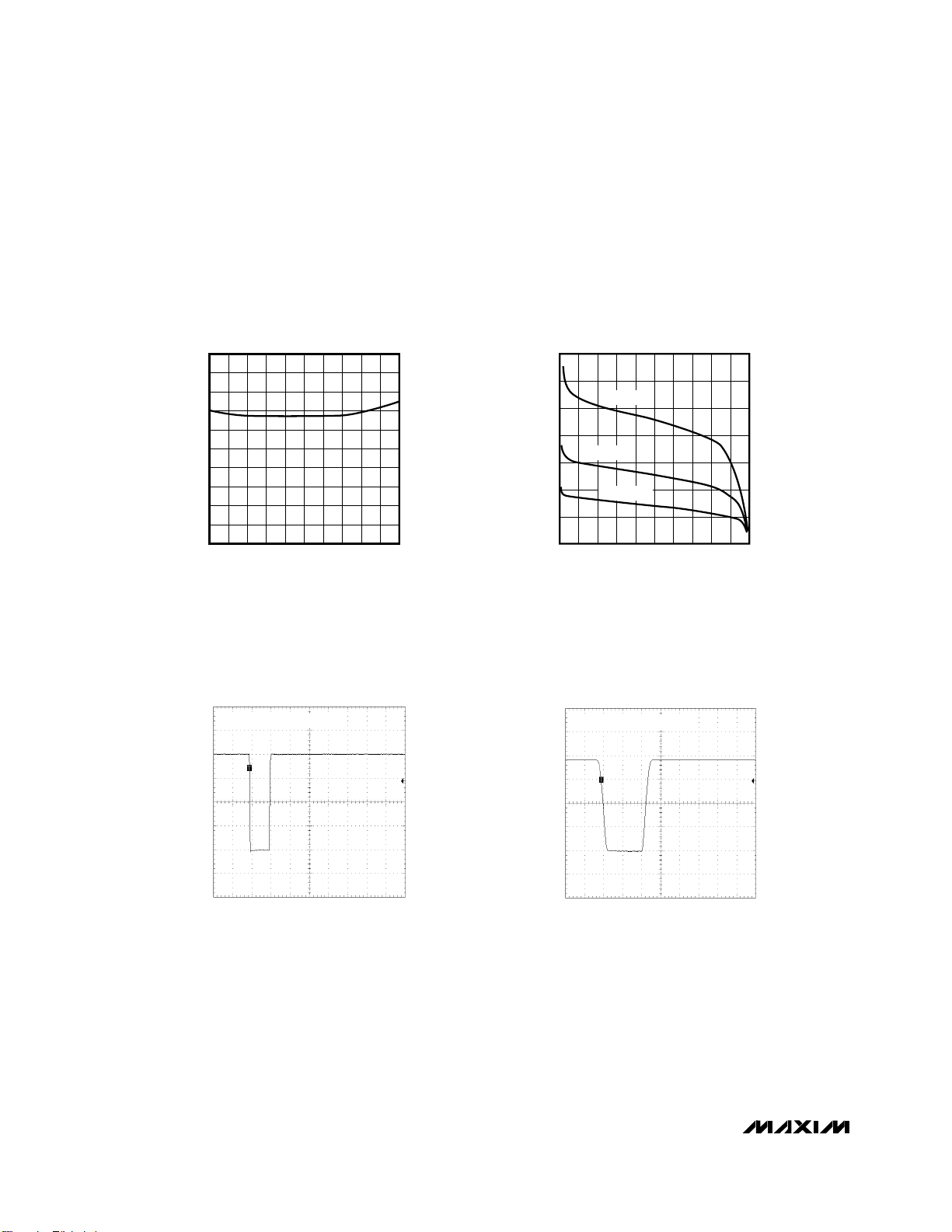
__________________________________________Typical Operating Characteristics
(V+ = +5V, TA = +25°C, unless otherwise noted.)
730
750
740
770
760
790
780
800
820
810
830
4.0 4.4 4.8 5.2 5.6 6.0
SCAN FREQUENCY vs.
POSITIVE SUPPLY VOLTAGE
MAX7219/21 01
POSITIVE SUPPLY VOLTAGE (V)
SCAN FREQUENCY (Hz)
0
20
10
40
30
60
50
70
012345
SEGMENT DRIVER OUTPUT CURRENT
vs. OUTPUT VOLTAGE
MAX7219/21 02
OUTPUT VOLTAGE (V)
OUTPUT CURRENT (mA)
R
SET
= 10k
Ω
R
SET
= 20k
Ω
R
SET
= 40k
Ω
MAX7219
SEGMENT OUTPUT CURRENT
MAX7219/21 03
5µs/div
10mA/div
0
MAXIMUM INTENSITY = 31/32
MAX7221
SEGMENT OUTPUT CURRENT
MAX7219/21 04
5µs/div
10mA/div
0
MAXIMUM INTENSITY = 15/16
Page 5
MAX7219/MAX7221
Serially Interfaced, 8-Digit LED Display Drivers
_______________________________________________________________________________________ 5
Pin Description
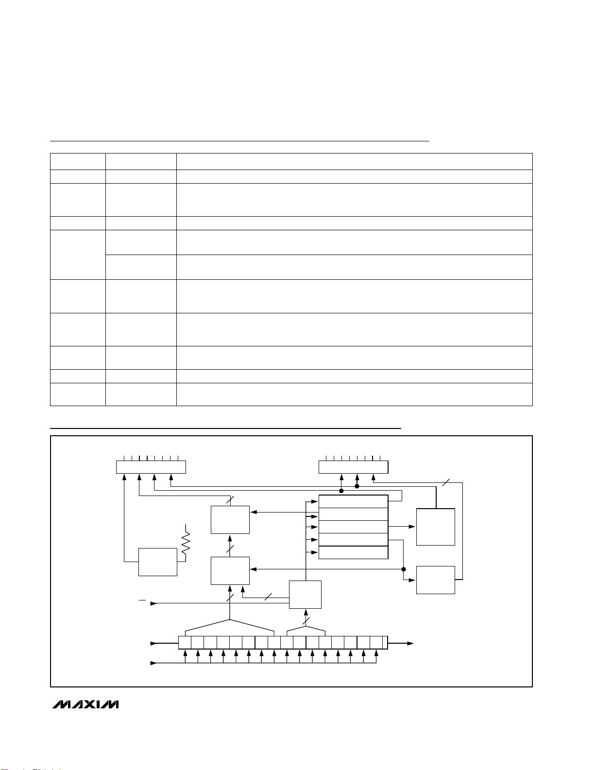
Functional Diagram
NAME FUNCTION
1 DIN Serial-Data Input. Data is loaded into the internal 16-bit shift register on CLK’s rising edge.
2, 3, 5–8,
10, 11
DIG 0–DIG 7
Eight-Digit Drive Lines that sink current from the display common cathode. The MAX7219 pulls
the digit outputs to V+ when turned off. The MAX7221’s digit drivers are high-impedance when
turned off.
PIN
4, 9 GND Ground (both GND pins must be connected)
12
LOAD
(MAX7219)
18 ISET
Connect to VDDthrough a resistor (R
SET
) to set the peak segment current (Refer to Selecting
R
SET
Resistor section).
14–17,
20–23
SEG A–SEG G,
DP
13 CLK
CS
(MAX7221)
24 DOUT
Serial-Data Output. The data into DIN is valid at DOUT 16.5 clock cycles later. This pin is used
to daisy-chain several MAX7219/MAX7221’s and is never high-impedance.
19 V+ Positive Supply Voltage. Connect to +5V.
Load-Data Input. The last 16 bits of serial data are latched on LOAD’s rising edge.
Chip-Select Input. Serial data is loaded into the shift register while CS is low. The last 16 bits of
serial data are latched on CS’s rising edge.
Serial-Clock Input. 10MHz maximum rate. On CLK’s rising edge, data is shifted into the internal shift register. On CLK’s falling edge, data is clocked out of DOUT. On the MAX7221, the
CLK input is active only while CS is low.
Seven Segment Drives and Decimal Point Drive that source current to the display. On the
MAX7219, when a segment driver is turned off it is pulled to GND. The MAX7221 segment drivers are high-impedance when turned off.
SEG A–SEG G, DP
SEGMENT DRIVERS
8
CODE B
ROM WITH
BYPASS
R
SET
D1 D2 D3 D4 D5 D6 D7 D8 D9 D10 D11 D12
8
8x8
DUAL-PORT
SRAM
8
ADDRESS
8
REGISTER
DECODER
LOAD (CS)
CLK
( ) MAX7221 ONLY
V+
SEGMENT
CURRENT
REFERENCE
DIN DOUT
D0
DIG 0–DIG 7
DIGIT DRIVERS
SHUTDOWN REGISTER
MODE REGISTER
INTENSITY REGISTER
SCAN-LIMIT REGISTER
DISPLAY-TEST REGISTER
4
D13 D14 D15
8
INTENSITY
PULSE-
WIDTH
MODULATOR
MULTIPLEX
SCAN
CIRCUITRY
(MSB)(LSB)
Page 6

MSB
MAX7219/MAX7221
Serially Interfaced, 8-Digit LED Display Drivers
6 _______________________________________________________________________________________
Detailed Description
MAX7219/MAX7221 Differences
The MAX7219 and MAX7221 are identical except for
two parameters: the MAX7221 segment drivers are
slew-rate limited to reduce electromagnetic interference (EMI), and its serial interface is fully SPI compatible.
Serial-Addressing Modes
For the MAX7219, serial data at DIN, sent in 16-bit
packets, is shifted into the internal 16-bit shift register
with each rising edge of CLK regardless of the state of
LOAD. For the MAX7221, CS must be low to clock data
in or out. The data is then latched into either the digit or
control registers on the rising edge of LOAD/CS.
LOAD/CS must go high concurrently with or after the
16th rising clock edge, but before the next rising clock
edge or data will be lost. Data at DIN is propagated
through the shift register and appears at DOUT 16.5
clock cycles later. Data is clocked out on the falling
edge of CLK. Data bits are labeled D0–D15 (Table 1).
D8–D11 contain the register address. D0–D7 contain
the data, and D12–D15 are “don’t care” bits. The first
received is D15, the most significant bit (MSB).
Digit and Control Registers
Table 2 lists the 14 addressable digit and control registers. The digit registers are realized with an on-chip,
8x8 dual-port SRAM. They are addressed directly so
that individual digits can be updated and retain data as
long as V+ typically exceeds 2V. The control registers
consist of decode mode, display intensity, scan limit
(number of scanned digits), shutdown, and display test
(all LEDs on).
Shutdown Mode
When the MAX7219 is in shutdown mode, the scan oscillator is halted, all segment current sources are pulled to
ground, and all digit drivers are pulled to V+, thereby
blanking the display. The MAX7221 is identical, except
the drivers are high-impedance. Data in the digit and
control registers remains unaltered. Shutdown can be
used to save power or as an alarm to flash the display by
successively entering and leaving shutdown mode. For
minimum supply current in shutdown mode, logic inputs
should be at ground or V+ (CMOS-logic levels).
Typically, it takes less than 250µs for the MAX7219/
MAX7221 to leave shutdown mode. The display driver
can be programmed while in shutdown mode, and
shutdown mode can be overridden by the display-test
function.
Figure 1. Timing Diagram
Table 1. Serial-Data Format (16 Bits)
D14D15
X
D12D13
XX
D10D11 D8D9
ADDRESS
D6D7 D4D5
X
D2D3 D0D1
MSB DATA LSB
CS
OR LOAD
t
CSS
CLK
t
DH
t
DS
DIN D15
DOUT
t
CL
t
CH
D14 D1 D0
t
CP
t
DO
t
CSH
t
CSW
t
LDCK
Page 7

Initial Power-Up
On initial power-up, all control registers are reset, the
display is blanked, and the MAX7219/MAX7221 enter
shutdown mode. Program the display driver prior to
display use. Otherwise, it will initially be set to scan one
digit, it will not decode data in the data registers, and
the intensity register will be set to its minimum value.
Decode-Mode Register
The decode-mode register sets BCD code B (0-9, E, H,
L, P, and -) or no-decode operation for each digit. Each
bit in the register corresponds to one digit. A logic high
selects code B decoding while logic low bypasses the
decoder. Examples of the decode mode control-register format are shown in Table 4.
When the code B decode mode is used, the decoder
looks only at the lower nibble of the data in the digit
registers (D3–D0), disregarding bits D4–D6. D7, which
sets the decimal point (SEG DP), is independent of the
decoder and is positive logic (D7 = 1 turns the decimal
point on). Table 5 lists the code B font.
When no-decode is selected, data bits D7–D0 correspond to the segment lines of the MAX7219/MAX7221.
Table 6 shows the one-to-one pairing of each data bit
to the appropriate segment line.
MAX7219/MAX7221
Serially Interfaced, 8-Digit LED Display Drivers
_______________________________________________________________________________________ 7
Table 2. Register Address Map
Table 3. Shutdown Register Format (Address (Hex) = 0xXC)
Table 4. Decode-Mode Register Examples (Address (Hex) = 0xX9)
No-Op X 0 0
0
0
0
ADDRESS
010xX0
0xX1
Digit 1 X 0 0
0
1
1
010xX2
0
0xX30Digit 2 X
Digit 3 X 0 1
1
0
Digit 0 X
0
010xX4
0xX5
Digit 5 X 0 1
1
1
1
010xX6
0
0xX70Digit 6 X
Digit 4 X
Digit 7 X 1 0
0
0
0
010xX8
0xX91
Decode
Mode
X
Intensity X 1 0
0
1
1
010xXA
0xXB
Shutdown X 1 1
1
0
1
010xXC
1
0xXF1
Display
Test
X
Scan Limit X
D15–
D12
D11 D10
REGISTER
D9 D8
HEX
CODE
X
Shutdown
Mode
0xXC X
X
XX
XX
XX
X
0X
1XXX
REGISTER DATA
MODE
Normal
Operation
0xXC
0No decode for digits 7–0 0
0
1
D7
DECODE MODE
0 0x000
0
1
D6 D5
0
1
D4 D3
0
1Code B decode for digits 7–0
Code B decode for digit 0
No decode for digits 7–1
0 0
0
1
D2
HEX
CODE
0
REGISTER DATA
0
0xFF
1
1
D1 D0
0
1
0
1
0 00
0x01
0
Code B decode for digits 3–0
No decode for digits 7–4
1 111 0x0F
ADDRESS CODE
(HEX)
D6 D4D7 D5 D2 D0D3 D1
Page 8

MAX7219/MAX7221
Intensity Control
and Interdigit Blanking
The MAX7219/MAX7221 allow display brightness to be
controlled with an external resistor (R
SET
) connected
between V+ and ISET. The peak current sourced from
the segment drivers is nominally 100 times the current
entering ISET. This resistor can either be fixed or variable to allow brightness adjustment from the front
panel. Its minimum value should be 9.53kΩ, which typically sets the segment current at 40mA. Display brightness can also be controlled digitally by using the
intensity register.
Digital control of display brightness is provided by an
internal pulse-width modulator, which is controlled by
the lower nibble of the intensity register. The modulator
scales the average segment current in 16 steps from a
maximum of 31/32 down to 1/32 of the peak current set
by R
SET
(15/16 to 1/16 on MAX7221). Table 7 lists the
intensity register format. The minimum interdigit blanking time is set to 1/32 of a cycle.
Serially Interfaced, 8-Digit LED Display Drivers
8 _______________________________________________________________________________________
Table 5. Code B Font
Table 6. No-Decode Mode Data Bits and
Corresponding Segment Lines
0 0X 00 0 11 11 11
D7*
REGISTER DATA
0
7-SEGMENT
CHARACTER
D3D6–D4 D1D2 DP*D0 BA DC FE G
1 0X 00 1 10
ON SEGMENTS = 1
01 00 0
2 0X 10 0 11 10 01 1
3 0X 10 1 11 11 00 1
4 0X 01 0 10 01 10 1
5 0X 01 1 01 11 10 1
6 0X 11 0 01 11 11 1
7 0X 11 1 11 01 00 0
8 1X 00 0 11 11 11 1
9 1X 00 1 11 11 10 1
— 1X 10 0 00 00 00 1
E 1X 10 1 01 10 11 1
H 1X 01 0 10 01 11 1
L 1X 01 1 00 10 11 0
P 1X 11 0 11 00 11 1
blank 1X 11 1 00 00 00 0
*The decimal point is set by bit D7 = 1
A
Corresponding
Segment Line
D6
DP C
D4
B
D5
E
D2
D G
REGISTER DATA
D0
F
D1D3D7
A
F
E
B
G
STANDARD 7-SEGMENT LED
C
D
DP
Page 9

Scan-Limit Register
The scan-limit register sets how many digits are displayed, from 1 to 8. They are displayed in a multiplexed
manner with a typical display scan rate of 800Hz with 8
digits displayed. If fewer digits are displayed, the scan
rate is 8f
OSC
/N, where N is the number of digits
scanned. Since the number of scanned digits affects
the display brightness, the scan-limit register should
not be used to blank portions of the display (such as
leading zero suppression). Table 8 lists the scan-limit
register format.
MAX7219/MAX7221
Serially Interfaced, 8-Digit LED Display Drivers
_______________________________________________________________________________________ 9
Table 7. Intensity Register Format (Address (Hex) = 0xXA)
DUTY CYCLE
MAX7221MAX7219
D6D7 D4 D2D3 D0D5 D1
HEX
CODE
1/16
(min on)
1/32
(min on)
XX XX 00 00 0xX0
2/163/32 XX XX 00 10 0xX1
3/165/32 XX XX 00 01 0xX2
4/167/32 XX XX 00 11 0xX3
5/169/32 XX XX 10 00 0xX4
6/1611/32 XX XX 10 10 0xX5
7/1613/32 XX XX 10 01 0xX6
X8/1615/32 XX X
X
10 11 0xX7
9/1617/32 XX X
X
01 00 0xX8
10/1619/32 XX X
X
01 10 0xX9
11/1621/32 XX X
X
01 01 0xXA
12/1623/32 XX X
X
01 11 0xXB
13/1625/32 XX X
X
11 00 0xXC
14/1627/32 XX X
X
11 10 0xXD
15/1629/32 XX X
X
11 01 0xXE
15/16
(max on)
31/32 XX X 11 11 0xXF
Table 8. Scan-Limit Register Format (Address (Hex) = 0xXB)
X
XDisplay digit 0 only*
Display digits 0 & 1*
X
X X
D7
SCAN LIMIT
0xX1
X 0xX0
X
X
X 0
D6 D5
0 1
D4 D3
X
XDisplay digits 0 1 2*
Display digits 0 1 2 3
X
X
X X
0
0xX3
X
D2
HEX
CODE
0xX2
0
REGISTER DATA
0
X
X
X
D1 D0
0 1 1
X 0 1 0
X
XDisplay digits 0 1 2 3 4
Display digits 0 1 2 3 4 5
X
X X 0xX5
X 0xX4
X
X
X 1 0 1
X
XDisplay digits 0 1 2 3 4 5 6
Display digits 0 1 2 3 4 5 6 7
X
X
X X
1
0xX7
X 0xX6
0 0
X
X
X 1 1 1
X 1 1 0
*See Scan-Limit Register section for application.
Page 10

MAX7219/MAX7221
If the scan-limit register is set for three digits or less,
individual digit drivers will dissipate excessive amounts
of power. Consequently, the value of the R
SET
resistor
must be adjusted according to the number of digits displayed, to limit individual digit driver power dissipation.
Table 9 lists the number of digits displayed and the
corresponding maximum recommended segment current when the digit drivers are used.
Display-Test Register
The display-test register operates in two modes: normal
and display test. Display-test mode turns all LEDs on
by overriding, but not altering, all controls and digit registers (including the shutdown register). In display-test
mode, 8 digits are scanned and the duty cycle is 31/32
(15/16 for MAX7221). Table 10 lists the display-test register format.
No-Op Register
The no-op register is used when cascading MAX7219s
or MAX7221s. Connect all devices’ LOAD/CS inputs
together and connect DOUT to DIN on adjacent
devices. DOUT is a CMOS logic-level output that easily
drives DIN of successively cascaded parts. (Refer to
the Serial Addressing Modes section for detailed infor-
mation on serial input/output timing.) For example, if
four MAX7219s are cascaded, then to write to the
fourth chip, sent the desired 16-bit word, followed by
three no-op codes (hex 0xXX0X, see Table 2). When
LOAD/CS goes high, data is latched in all devices. The
first three chips receive no-op commands, and the
fourth receives the intended data.
Applications Information
Supply Bypassing and Wiring
To minimize power-supply ripple due to the peak digit
driver currents, connect a 10µF electrolytic and a 0.1µF
ceramic capacitor between V+ and GND as close to
the device as possible. The MAX7219/MAX7221 should
be placed in close proximity to the LED display, and
connections should be kept as short as possible to
minimize the effects of wiring inductance and electromagnetic interference. Also, both GND pins must be
connected to ground.
Selecting R
SET
Resistor and
Using External Drivers
The current per segment is approximately 100 times
the current in ISET. To select R
SET
, see Table 11. The
MAX7219/MAX7221’s maximum recommended segment current is 40mA. For segment current levels
above these levels, external digit drivers will be needed. In this application, the MAX7219/MAX7221 serve
only as controllers for other high-current drivers or transistors. Therefore, to conserve power, use R
SET
= 47kΩ
when using external current sources as segment drivers.
The example in Figure 2 uses the MAX7219/MAX7221’s
segment drivers, a MAX394 single-pole double-throw
analog switch, and external transistors to drive 2.3”
AND2307SLC common-cathode displays. The 5.6V
zener diode has been added in series with the decimal
point LED because the decimal point LED forward voltage is typically 4.2V. For all other segments the LED
forward voltage is typically 8V. Since external transistors are used to sink current (DIG 0 and DIG 1 are used
as logic switches), peak segment currents of 45mA are
allowed even though only two digits are displayed. In
applications where the MAX7219/MAX7221’s digit drivers are used to sink current and fewer than four digits
are displayed, Table 9 specifies the maximum allowable segment current. R
SET
must be selected accord-
ingly (Table 11).
Refer to the Power Dissipation section of the Absolute
Maximum Ratings to calculate acceptable limits for
ambient temperature, segment current, and the LED
forward-voltage drop.
Serially Interfaced, 8-Digit LED Display Drivers
10 ______________________________________________________________________________________
Table 9. Maximum Segment Current for
1-, 2-, or 3-Digit Displays
Table 10. Display-Test Register Format
(Address (Hex) = 0xXF)
10
202
MAXIMUM SEGMENT
CURRENT
(mA)
1
303
NUMBER OF DIGITS
DISPLAYED
X
X
Normal
Operation
D6
X X
Display Test
Mode
D4
X
X
D5
X
X
D2
X 0
REGISTER DATA
D0
X
X X
D1
X
D3
1X
D7
MODE
Note: The MAX7219/MAX7221 remain in display-test mode
(all LEDs on) until the display-test register is reconfigured
for normal operation.
Page 11

Computing Power Dissipation
The upper limit for power dissipation (PD) for the
MAX7219/MAX7221 is determined from the following
equation:
PD = (V + x 8mA) + (V+ - V
LED
)(DUTY x I
SEG
x N)
where:
V+ = supply voltage
DUTY = duty cycle set by intensity register
N = number of segments driven (worst case is 8)
V
LED
= LED forward voltage
I
SEG
= segment current set by R
SET
Dissipation Example:
I
SEG
= 40mA, N = 8, DUTY = 31/32, V
LED
= 1.8V at
40mA, V+ = 5.25V
PD = 5.25V(8mA) + (5.25V - 1.8V)(31/32 x
40mA x 8) = 1.11W
Thus, for a CERDIP package (θJA= +80°C/W from
Table 12), the maximum allowed ambient temperature
TAis given by:
T
J(MAX)
= TA+ PD x θJA+ 150°C = TA+1.11W x
80°C/W
where TA= +61.2°C.
The TAlimits for PDIP and SO Packages in the dissipation
example above are +66.7°C and +55.6°C, respectively.
Cascading Drivers
The example in Figure 3 drives 16 digits using a 3-wire
µP interface. If the number of digits is not a multiple of
8, set both drivers’ scan limits registers to the same
number so one display will not appear brighter than the
other. For example, if 12 digits are need, use 6 digits
per display with both scan-limit registers set for 6 digits
so that both displays have a 1/6 duty cycle per digit. If
11 digits are needed, set both scan-limit registers for 6
digits and leave one digit driver unconnected. If one
display for 6 digits and the other for 5 digits, the second display will appear brighter because its duty cycle
per digit will be 1/5 while the first display’s will be 1/6.
Refer to the No-Op Register section for additional information.
MAX7219/MAX7221
Serially Interfaced, 8-Digit LED Display Drivers
______________________________________________________________________________________ 11
Table 11. R
SET
vs. Segment Current and
LED Forward Voltage
Table 12. Package Thermal Resistance
Data
12.2
17.8
1.5
40 11.0
2.5
11.8
30
9.69
15.8
V
LED
(V)
10.6
29.8
2.0
66.7
20
17.1 14.0
25.9
15.0
28.0
10
3.5
22.6
59.3
3.0
I
SEG
(mA)
24.5
63.7 51.255.4
24 Narrow DIP
24 Wide SO
PACKAGE
+85°C/W
24 CERDIP
Maximum Ambient Temperature (TA) = +85°C
Maximum Junction Temperature (TJ) = +150°C
+80°C/W
THERMAL RESISTANCE
(
θθ
JA
)
+75°C/W
Page 12

MAX7219/MAX7221
Serially Interfaced, 8-Digit LED Display Drivers
12 ______________________________________________________________________________________
Figure 2. MAX7219/MAX7221 Driving 2.3in Displays
AND2307SLC
ANODE DP
ANODE A
ANODE F
ANODE B
ANODE G
ANODE C
ANODE E
ANODE D
1N5524B
5.6V ±5%
5
7
9
6
10
4
2
3
23
SEG D
21
SEG E
20
SEG C
17
SEG G
16
SEG B
15
SEG F
14
SEG A
22
SEG DP
4
GND
9
GND
DATA IN
LOAD (CS)
CLOCK
1
12
13
DIN
LOAD (CS)
CLK
ANODE DP
ANODE A
ANODE F
ANODE B
ANODE G
ANODE C
ANODE E
ANODE D
4.7kΩ
4.7kΩ
COM1
COM2
AND2307SLC
CATHODE
3
IRF540
8
5
7
9
6
10
4
2
CATHODE
88
MAX7219
MAX7221
I
SFT
DIG 0
DIG 1
19
V+
30kΩ
18
*
*
2
11
10
3
5V
0.1µF
16
4
NC1
7
NC2
1
IN1
MAX394
IN2
2
NO1
9
NO2
5
*4.7kΩ PULLUP REQUIRED FOR MAX7221
( ) MAX7221 ONLY
-5V
IRF540
Page 13

MAX7219/MAX7221
Serially Interfaced, 8-Digit LED Display Drivers
______________________________________________________________________________________ 13
Figure 3. Cascading MAX7219/MAX7221s to Drive 16 Seven-Segment LED Digits
88
DATA IN
LOAD DATA
( ) MAX7221 ONLY CLOCK
DIN
DIG 0
DIG 4
DIG 6
DIG 2
DIG 3
GND
DIG 5
DIG 1
LOAD (CS)
DOUT
SEG D
SEG DP
SEG EGND
SEG C
ISET
SEG GDIG 7
SEG B
SEG F
SEG A
CLK
5V
V+
9.53kΩ
0.1µF
MAX7219
MAX7221
DIN
DIG 0
DIG 4
DIG 6
DIG 2
DIG 3
GND
DIG 5
DIG 1
LOAD (CS)
DOUT
SEG D
SEG DP
SEG EGND
SEG C
ISET
SEG GDIG 7
SEG B
SEG F
SEG A
CLK
88
5V
V+
9.53kΩ
0.1µF
MAX7219
MAX7221
Page 14

MAX7219/MAX7221
Serially Interfaced, 8-Digit LED Display Drivers
14 ______________________________________________________________________________________
Ordering Information (continued) Chip Topography
PART
MAX7221CNG
MAX7221CWG
MAX7221C/D 0°C to +70°C
0°C to +70°C
0°C to +70°C
TEMP RANGE PIN-PACKAGE
24 Narrow Plastic DIP
24 Wide SO
Dice*
MAX7221ENG
MAX7221EWG
MAX7221ERG -40°C to +85°C
-40°C to +85°C
-40°C to +85°C 24 Narrow Plastic DIP
24 Wide SO
24 Narrow CERDIP
*Dice are specified at TA= +25°C.
TRANSISTOR COUNT: 5267
SUBSTRATE CONNECTED TO GND
GND
DIG 5
DIG 1
LOAD
OR
CS
CLK
SEG A
SEG F
SEG B ISET
DIG 7
SEG G
DIG 3 DIG 2
SEG C
0.080"
(2.03mm)
DIG 6
SEG E
GND
SEG DP
DIG 4
DIG 0
DIN
DOUT
SEG D
0.093"
(2.36mm)
Page 15

MAX7219/MAX7221
Serially Interfaced, 8-Digit LED Display Drivers
______________________________________________________________________________________ 15
Package Information
(The package drawing(s) in this data sheet may not reflect the most current specifications. For the latest package outline information
go to www.maxim-ic.com/packages
.)
N
1
TOP VIEW
D
e
FRONT VIEW
INCHES
MIN
DIM
0.093A
0.004
A1
0.014
B
0.009
C
H
E
A
B
A1
C
L
e 0.050 1.27
0.291
E
H 0.4190.394 10.00 10.65
0.016L
VARIATIONS:
INCHES
MINDIM
D
0.398 0.413 AA10.5010.10 16
D
0.447 0.463 AB11.7511.35 18
D 0.6140.598 15.20 2415.60 AD
D 0.7130.697 17.70 2818.10 AE
0-8
SIDE VIEW
MAX
0.104
0.012
0.019
0.013
0.299
0.050
MAX
0.5120.496D
MILLIMETERS
MAX
MIN
2.65
2.35
0.30
0.10
0.49
0.35
0.23
0.32
7.40 7.60
0.40 1.27
MILLIMETERS
MAX
MIN
12.60 13.00
N MS013
20
AC
SOICW.EPS
PROPRIETARY INFORMATION
TITLE:
PACKAGE OUTLINE, .300" SOIC
REV.DOCUMENT CONTROL NO.APPROVAL
21-0042
1
B
1
Page 16

Maxim cannot assume responsibility for use of any circuitry other than circuitry entirely embodied in a Maxim product. No circuit patent licenses are
implied. Maxim reserves the right to change the circuitry and specifications without notice at any time.
16 __________________Maxim Integrated Products, 120 San Gabriel Drive, Sunnyvale, CA 94086 (408) 737-7600
© 2003 Maxim Integrated Products Printed USA is a registered trademark of Maxim Integrated Products.
MAX7219/MAX7221
Serially Interfaced, 8-Digit LED Display Drivers
MAX7219/MAX7221
Package Information (continued)
(The package drawing(s) in this data sheet may not reflect the most current specifications. For the latest package outline information
go to www.maxim-ic.com/packages
.)
PDIPN.EPS
 Loading...