

Page 1
现货库存、技术资料、百科信息、热点资讯,精彩尽在鼎好!
General Description
The MAX706P/R/S/T, MAX706AP/AR/AS/AT, and
MAX708R/S/T microprocessor (µP) supervisory circuits
reduce the complexity and number of components
required to monitor +3V power-supply levels in +3V to
+5V µP systems. These devices significantly improve
system reliability and accuracy compared to separate
ICs or discrete components.
The MAX706P/R/S/T and MAX706AP/AR/AS/AT supervisory circuits provide the following four functions:
1) A reset output during power-up, power-down, and
brownout conditions.
2) An independent watchdog output that goes low if the
watchdog input has not been toggled within 1.6s.
3) A 1.25V threshold detector for power-fail warning,
low-battery detection, or for monitoring a power
supply other than the main supply.
4) An active-low, manual-reset input.
The only difference between the MAX706R/AR,
MAX706S/AS, and MAX706T/AT is the reset-threshold
voltage levels, which are 2.63V, 2.93V, and 3.08V,
respectively. All have active-low reset output signals.
The MAX706P/AP are identical to the MAX706R/AR,
except the reset output signal is active-high. The watchdog timer function for the MAX706AP/AR/AS/AT disables when the WDI input is left open or connected to a
high-impedance state of a low-leakage tri-state output.
The MAX708R/S/T provide the same functions as the
MAX706R/S/T and MAX706AR/AS/AT except they do
not have a watchdog timer. Instead, they provide both
RESET and RESET outputs. As with the MAX706,
devices with R, S, and T suffixes have reset thresholds
of 2.63V, 2.93V, and 3.08V, respectively.
These devices are available in 8-pin SO, DIP, and
µMAX®packages and are fully specified over the operating temperature range.
Applications
Battery-Powered Equipment
Portable Instruments
Computers
Controllers
Intelligent Instruments
Critical µP Power Monitoring
Features
♦ µMAX Package, Small 8-Pin SO
♦ Precision Supply-Voltage Monitors
2.63V (MAX706P/R, MAX706AP/AR, and MAX708R)
2.93V (MAX706S, MAX706AS, and MAX708S)
3.08V (MAX706T, MAX706AT, and MAX708T)
♦ 200ms Reset Time Delay
♦ Debounced TTL/CMOS-Compatible Manual Reset
Input
♦ 100µA Quiescent Current
♦ WDI Disable Feature (MAX706AP/AR/AS/AT)
♦ Watchdog Timer: 1.6s Timeout
♦ Reset Output Signal:
Active-High Only (MAX706P, MAX706AP)
Active-Low Only (MAX706R/S/T, MAX706AR/AS/AT)
Active-High and Active-Low (MAX708R/S/T)
♦ Voltage Monitor for Power-Fail or Low-Battery
Warning
♦ 8-Pin Surface-Mount Package
♦ Guaranteed RESET Assertion to V
CC
= 1V
MAX706P/R/S/T, MAX706AP/AR/AS/AT, MAX708R/S/T
+3V Voltage Monitoring, Low-Cost µP
Supervisory Circuits
________________________________________________________________ Maxim Integrated Products 1
Ordering Information
19-0099; Rev 5; 4/06
For pricing, delivery, and ordering information, please contact Maxim/Dallas Direct! at
1-888-629-4642, or visit Maxim’s website at www.maxim-ic.com.
Ordering Information continued at end of data sheet.
Pin Configurations appear at end of data sheet.
µMAX is a registered trademark of Maxim Integrated Products, Inc.
PART†
TEMP
RANGE
PIN-
PKG
CODE
MAX706PCPA
0°C to +70°C 8 PDIP P8-1
MAX706PCSA
0°C to +70°C 8 SO S8-2
MAX706PCUA
0°C to +70°C 8 µMAX U8-1
MAX706PEPA
8 PDIP P8-1
†
SO, µMAX, and PDIP packages are available in lead-free.
V
CC
PFI
GND
MR
PFO
WDO
RESET
UNREGULATED
DC
PUSHBUTTON
SWITCH
WDI
I/O LINE
INTERRUPT
µP
MAX639
DC-DC
CONVERTER
+3V/+3.3V
MAX706R/S/T
MAX706AR/AS/AT
V
CC
RESET
NMI
Typical Operating Circuits
Typical Operating Circuits continued at end of data sheet.
PACKAGE
-40°C to +85°C
Page 2
MAX706P/R/S/T, MAX706AP/AR/AS/AT, MAX708R/S/T
+3V Voltage Monitoring, Low-Cost µP
Supervisory Circuits
2 _______________________________________________________________________________________
ABSOLUTE MAXIMUM RATINGS
ELECTRICAL CHARACTERISTICS
(MAX70_P/R, MAX706AP/AR: VCC= 2.7V to 5.5V; MAX70_S, MAX706AS: V
CC
= 3.0V to 5.5V; MAX70_T, MAX706AT: V
CC
= 3.15V to
5.5V; T
J
= TA= T
MIN
to T
MAX
, unless otherwise noted. Typical values are at TJ= TA= +25°C.) (Note 2)
Stresses beyond those listed under “Absolute Maximum Ratings” may cause permanent damage to the device. These are stress ratings only, and functional
operation of the device at these or any other conditions beyond those indicated in the operational sections of the specifications is not implied. Exposure to
absolute maximum rating conditions for extended periods may affect device reliability.
Terminal Voltage (with respect to GND)
V
CC
........................................................................-0.3V to +6V
All Other Inputs (Note 1)..........................-0.3V to (V
CC
+ 0.3V)
Input Current
V
CC
..................................................................................20mA
GND .................................................................................20mA
Output Current (all outputs) ................................................20mA
Continuous Power Dissipation (T
A
= +70°C)
8-Pin CERDIP (derate 8mW/°C above +70°C)..............640mW
8-Pin PDIP (derate 9.1mW/°C above +70°C).............727.3mW
8-Pin SO (derate 5.9mW/°C above +70°C)................470.6mW
8-Pin µMAX (derate 4.5mW/
o
C above +70°C) ..............362mW
Operating Temperature Range
MAX70_C .............................................................0°C to +70°C
MAX70_E ..........................................................-40°C to +85°C
MAX70_M .......................................................-55°C to +125°C
Junction Temperature......................................................+150°C
Storage Temperature Range .............................-65°C to +150°C
Lead Temperature (soldering, 10s) .................................+300°C
Note 1: The input-voltage limits on PFI, WDI, and MR can be exceeded if the input current is less than 10mA.
PARAMETER
SYMBOL
CONDITIONS
MIN
TYP
MAX
UNITS
MAX70_C 1.0 5.5
Supply Voltage Range V
CC
MAX70_E/M 1.2 5.5
V
MAX706_C 90 200
MAX706_E/M 90 300
MAX708_C 50 200
VCC < 3.6V
MAX708_E/M 50 300
MAX706_C
350
MAX706_E/M
500
MAX708_C 65 350
Supply Current
VCC < 5.5V
MAX708_E/M 65 500
µA
MAX70_P/R/, MAX706AP/AR
MAX70_S, MAX706AS
Reset Threshold (Note 3)
(V
CC
Falling)
V
RST
MAX70_T, MAX706AT
V
Reset Threshold Hysteresis
(Note 3)
V
HYS
20 mV
MAX70_P/R/, MAX706AP/AR VCC = 3.0V
280
MAX70_S, MAX706AS, VCC = 3.3V
280Reset Pulse Width (Note 3) t
RST
VCC = 5V
ms
RESET OUTPUT
V
OH
)
0.8 x
V
OL
)
I
SINK
= 1.2mA 0.3
V
OH
4.5V < VCC < 5.5V
I
RSOURCE
=
800µA
VCC -
1.5
V
OL
4.5V < V
CC
< 5.5V I
SINK
= 3.2mA 0.4
MAX70_C VCC = 1.0V, I
SINK
= 50µA 0.3
Output-Voltage High
(MAX70_R/S/T)
(MAX706AR/AS/AT)
V
OL
MAX70_E/M: VCC = 1.2V, I
SINK
= 100µA 0.3
V
I
SUPPLY
V
RST(MAX
V
RST(MAX
< VCC < 3.6V I
< VCC < 3.6V
SOURCE
= 500µA
135
135
2.55 2.63 2.70
2.85 2.93 3.00
3.00 3.08 3.15
140 200
140 200
200
V
CC
Page 3
MAX706P/R/S/T, MAX706AP/AR/AS/AT, MAX708R/S/T
+3V Voltage Monitoring, Low-Cost µP
Supervisory Circuits
_______________________________________________________________________________________ 3
ELECTRICAL CHARACTERISTICS (continued)
(MAX70_P/R, MAX706AP/AR: VCC= 2.7V to 5.5V; MAX70_S, MAX706AS: V
CC
= 3.0V to 5.5V; MAX70_T, MAX706AT: V
CC
= 3.15V to
5.5V; T
J
= TA= T
MIN
to T
MAX
, unless otherwise noted. Typical values are at TJ= TA= +25°C.) (Note 2)
PARAMETER
SYMBOL
CONDITIONS
MIN
TYP
MAX
UNITS
V
OH
)
VCC -
0.6
V
OL
)
I
SINK
= 1.2mA 0.3
V
OH
4.5 < VCC < 5.5V
VCC -
1.5
Output-Voltage High
(MAX706P) (MAX706AP)
V
OL
4.5V < VCC < 5.5V I
SINK
= 3.2mA 0.4
V
V
OH
)
V
OL
)
I
SINK
= 500µA 0.3
V
OH
4.5V < VCC < 5.5V
VCC -
1.5
Output-Voltage High
(MAX708_)
V
OL
4.5V < VCC < 5.5V I
SINK
= 1.2mA 0.4
V
WATCHDOG INPUT
MAX706P/R, MAX706AP/AR, VCC = 3.0V
Watchdog Timeout Period t
WD
MAX706S/T, MAX706AS/AT, VCC = 3.3V
s
VIL = 0.4V
V
RST(MAX)
< V
CC
< 3.6V
WDI Pulse Width
(MAX706_, MAX706A_)
t
WP
VIH = 0.8V x V
CC
4.5V < VCC <
5.5V
50
ns
V
IL
V
RST(MAX)
< VCC < 3.6V 0.6
V
IH
V
RST(MAX)
< VCC < 3.6V
0.7 x
V
IL
V
CC
= 5.0V 0.8
Watchdog Input Threshold
(MAX706_, MAX706A_)
V
IH
V
CC
= 5.0V 3.5
V
MAX706_
WDI Input Current WDI = 0V or V
CC
MAX706A_ -5 +5
µA
V
RST(MAX
V
RST(MAX
V
RST(MAX
V
RST(MAX
< VCC < 3.6V I
< VCC < 3.6V
< VCC < 3.6V I
< VCC < 3.6V
= 215µA
SOURCE
I
I
SOURCE
SOURCE
SOURCE
= 800µA
= 500µA 0.8 x V
= 800µA
CC
1.00 1.60 2.25
1.00 1.60 2.25
100
V
CC
-1.0 +0.02 +1.0
Page 4
MAX706P/R/S/T, MAX706AP/AR/AS/AT, MAX708R/S/T
+3V Voltage Monitoring, Low-Cost µP
Supervisory Circuits
4 _______________________________________________________________________________________
ELECTRICAL CHARACTERISTICS (continued)
(MAX70_P/R, MAX706AP/AR: VCC= 2.7V to 5.5V; MAX70_S, MAX706AS: V
CC
= 3.0V to 5.5V; MAX70_T, MAX706AT: V
CC
= 3.15V to
5.5V; T
J
= TA= T
MIN
to T
MAX
, unless otherwise noted. Typical values are at TJ= TA= +25°C.) (Note 2)
PARAMETER
CONDITIONS
UNITS
WATCHDOG OUTPUT
V
OH
)
0.8 x
V
OL
)
I
SINK
= 500µA 0.3
V
OH
4.5V < VCC < 5.5V
VCC -
1.5
WDO Output Voltage
(MAX706_, MAX706A_)
V
OL
4.5V < VCC < 5.5V I
SINK
= 1.2mA 0.4
V
MANUAL RESET INPUT
V
RST(MAX)
< V
CC
< 3.6V
25 70 250
MR Pullup Current MR = 0
4.5V < V
CC
<
5.5V
600
µA
V
RST(MAX)
< VCC < 3.6V
MR Pulse Width t
MR
4.5V < VCC < 5.5V
ns
V
IL
V
RST(MAX)
< VCC < 3.6V 0.6
V
IH
V
RST(MAX)
< VCC < 3.6V
0.7 x
V
IL
4.5V < VCC < 5.5V 0.8
MR Input Threshold
V
IH
4.5V < VCC < 5.5V 2.0
V
V
RST(MAX)
< VCC < 3.6V 750
MR to Reset Output Delay t
MD
4.5V < VCC < 5.5V 250
ns
POWER-FAILURE COMPARATOR
(MAX70_P/R, MAX706AP/AR) PFI falling
V
CC
= 3.0V
PFI Input Threshold
(MAX70_S/T, MAX706AS/AT) PFI falling,
V
CC
= 3.3V
V
PFI Input Current -25
nA
V
OH
)
0.8 x
V
OL
)
I
SINK
= 1.2mA 0.3
V
OH
4.5V < VCC < 5.5V
VCC -
1.5
PFO Output Voltage
V
OL
4.5V < VCC < 5.5V I
SINK
= 3.2mA 0.4
V
Note 2: All devices 100% production tested at TA= +85°C. Limits over temperature are guaranteed by design.
Note 3: Applies to both RESET in the MAX70_R/S/T and MAX706AR/AS/AT, and RESET in the MAX706P/MAX706AP.
SYMBOL
MIN TYP MAX
V
RST(MAX
V
RST(MAX
< VCC < 3.6V I
< VCC < 3.6V
SOURCE
I
SOURCE
= 500µA
= 800µA
V
RST(MAX
V
RST(MAX
< VCC < 3.6V I
< VCC < 3.6V
SOURCE
I
SOURCE
= 500µA
= 800µA
V
CC
100 250
500
150
V
CC
1.20 1.25 1.30
1.20 1.25 1.30
+0.01 +25
V
CC
Page 5
MAX706P/R/S/T, MAX706AP/AR/AS/AT, MAX708R/S/T
+3V Voltage Monitoring, Low-Cost µP
Supervisory Circuits
_______________________________________________________________________________________ 5
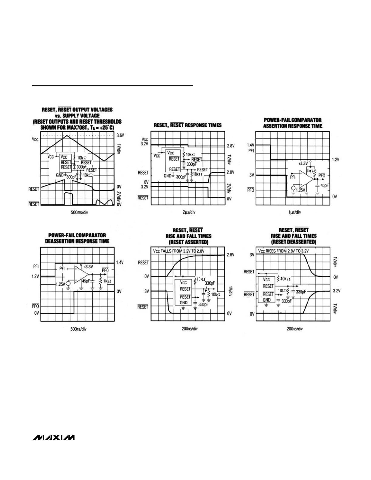
Typical Operating Characteristics
(TA = +25°C, unless otherwise noted.)
Typical Operating Characteristics
Page 6

MAX706P/R/S/T, MAX706AP/AR/AS/AT, MAX708R/S/T
+3V Voltage Monitoring, Low-Cost µP
Supervisory Circuits
6 _______________________________________________________________________________________
Pin Description
PIN
MAX706P
MAX706AP
MAX706R/S/T,
SO/DIP
FUNCTION
131313
Acti ve-Low , M anual -Reset Inp ut. P ull M R b el ow 0.6V to tr i gg er a
r eset pul se. M R i s TTL/C M OS com p ati b l e w hen V
C C
= 5V and can
b e shorted to GN D wi th a swi tch. M R i s i nter nal l y connected to a
70µA sour ce curr ent. C onnect to V
C C
or l eave unconnected .
242424
S upp l y V ol tag e Inp ut
353535
Ground
464646
Adjustable Power-Fail Comparator Input. Connect PFI to a
resistive divider to set the desired PFI threshold. When PFI is
less than 1.25V, PFO goes low and sinks current; otherwise,
PFO remains high. Connect PFI to GND if not used.
575757
Active-Low, Power-Fail Comparator Output. PFO asserts when
PFI is below the internal 1.25V threshold. PFO deasserts when
PFI is above the internal 1.25V threshold. Leave PFO
unconnected if not used.
6868——
Watchdog Input. A falling or rising transition must occur at
WDI within 1.6s to prevent WDO from asserting (see Figure 4).
The internal watchdog timer is reset to zero when reset is
asserted or when transition occurs at WDI. The watchdog
function for the MAX706P/R/S/T can not be disabled. The
watchdog timer for the MAX706AP/AR/AS/AT disables when
WDI input is left open or connected to a tri-state output in its
high-impedance state with a leakage current of less than
600nA.
71——82
Active-High Reset Output. Reset remains high when VCC is
below the reset threshold or MR is held low. It remains low for
200ms after the reset conditions end (Figure 3).
8282——
Active-Low Watchdog Output. WDO goes low when a
transition does not occur at WDI within 1.6s and remains low
until a transition occurs at WDI (indicating the watchdog
interrupt has been serviced). WDO also goes low when V
CC
falls below the reset threshold; however, unlike the reset
output signal, WDO goes high as soon as V
CC
rises above
the reset threshold.
——7 171
Active-Low Reset Output. RESET remains low when VCC is
below the reset threshold or MR is held low. It remains low for
200ms after the reset conditions end (Figure 3).
————68
No Connection. Not internally connected.
MAX706AR/AS/AT
µMAX SO/DIP µMAX SO/DIP µMAX
MAX708R/S/T
NAME
MR
V
C C
GND
PFI
PFO
WDI
RESET
WDO
RESET
N.C.
Page 7

MAX706P/R/S/T, MAX706AP/AR/AS/AT, MAX708R/S/T
+3V Voltage Monitoring, Low-Cost µP
Supervisory Circuits
_______________________________________________________________________________________ 7
RESET and
RESET
Outputs
A microprocessor’s (µP’s) reset input starts in a known
state. When the µP is in an unknown state, it should be
held in reset. The MAX706P/R/S/T and the MAX706AP/
AR/AS/AT assert reset when VCCis low, preventing
code execution errors during power-up, power-down,
or brownout conditions.
On power-up once VCCreaches 1V, RESET is guaranteed to be logic-low and RESET is guaranteed to be
logic-high. As VCCrises, RESET and RESET remain
asserted. Once VCCexceeds the reset threshold, the
internal timer causes RESET and RESET to be
deasserted after a time equal to the reset pulse width,
which is typically 200ms (Figure 3).
If a power-fail or brownout condition occurs (i.e., V
CC
drops below the reset threshold), RESET and RESET
are asserted. As long as VCCremains below the reset
threshold, the internal timer is continually reset, causing
the RESET and RESET outputs to remain asserted.
Thus, a brownout condition that interrupts a previously
initiated reset pulse causes an additional 200ms delay
from the time the latest interruption occurred. On
power-down once VCCdrops below the reset threshold,
RESET and RESET are guaranteed to be asserted for
VCC≥ 1V.
The MAX706P/MAX706AP provide a RESET signal, and
the MAX706R/S/T and MAX706AR/AS/AT provide a
RESET signal. The MAX708R/S/T provide both RESET
and RESET.
Watchdog Timer
The MAX706P/R/S/T and the MAX706AP/AR/AS/AT
watchdog circuit monitor the µP’s activity. If the µP
does not toggle the watchdog input (WDI) within 1.6s,
the watchdog output (WDO) goes low (Figure 4). If the
reset signal is asserted, the watchdog timer will be
reset to zero and disabled. As soon as reset is
released, the timer starts counting. WDI can detect pulses as narrow as 100ns with a 2.7V supply and 50ns with a
4.5V supply. The watchdog timer for the MAX706P/R/S/T
cannot be disabled. The watchdog timer for the
MAX706AP/AR/AS/AT operates similarly to the
MAX706P/R/S/T. However, the watchdog timer for the
MAX706AP/AR/AS/AT disables when the WDI input is
left open or connected to a tri-state output in its highimpedance state and with a leakage current of less
than 600nA. The watchdog timer can be disabled anytime, provided WDO is not asserted.
RESET
GENERATOR
V
CC
70µA
8
7
RESET
RESET
5
PFO
GND
3
1.25V
2.63V MAX708R
2.93V MAX708S
3.08V MAX708T
1
MR
2
V
CC
4
PFI
MAX708R/S/T
Figure 1. MAX706_ Functional Diagram
Figure 2. MAX708_ Functional Diagram
WATCHDOG
TRANSITION
DETECTOR
WATCHDOG
TIMER
TIMEBASE FOR
RESET AND
WATCHDOG
RESET
GENERATOR
V
CC
70µA
8
WDO
7
RESET
(RESET)
5
PFO
GND
3
1.25V
2.63V MAX706P/R
2.93V MAX706S
3.08V MAX706T
( ) ARE FOR MAX706P/AP.
6
WDI
1
MR
2
V
CC
4
PFI
MAX706P/R/S/T
MAX706AP/AR/AS/AT
Page 8

MAX706P/R/S/T, MAX706AP/AR/AS/AT, MAX708R/S/T
+3V Voltage Monitoring, Low-Cost µP
Supervisory Circuits
8 _______________________________________________________________________________________
WDO can be connected to the nonmaskable interrupt
(NMI) input of a µP. When V
CC
drops below the reset
threshold, WDO immediately goes low, even if the
watchdog timer has not timed out (Figure 3). Normally,
this would trigger an NMI, but since reset is asserted
simultaneously, the NMI is overridden. The WDO
should not be connected to RESET directly. Instead,
connect WDO to MR to generate a reset pulse when it
times out.
Manual Reset
The manual reset (MR) input allows RESET and RESET
to be activated by a pushbutton switch. The switch is
effectively debounced by the 140ms minimum reset
pulse width. MR can be driven by an external logic line
since it is TTL/CMOS compatible. The minimum MR
input pulse width is 500ns when VCC= +3V and 150ns
when VCC= +5V. Leave MR unconnected or connect
to V
CC
when not used.
Power-Fail Comparator
The power-fail comparator can be used for various purposes because its output and noninverting input are
not internally connected. The inverting input is internally
connected to a 1.25V reference. The power-fail comparator has 10mV of hysteresis, which prevents repeated triggering of the power-fail output (PFO).
t
RST
t
RST
+3.3V
0V
+3.3V
+1V
0V
RESET
RESET
WDO*
+3.3V
0V
MR*
t
MR
*NOTE: MR EXTERNALLY DRIVEN LOW.
WDO TIMING SHOWN FOR MAX706P/R/S/T.
+3.3V
0V
V
CC
V
RSTVRST
t
MD
MAX706_
MAX708R/S/T
RESET
(RESET)
130kΩ
1%
PARAMETER
MIN TYP
MAX UNIT
+12V RESET
THRESHOLD AT +25°C
10.24
10.87
11.50 V
1MΩ
1%
+3V/+3.3V
+12V
V
CC
PFI
( ) ARE FOR MAX706P/AP
GND
MR
PFO
TO µP
Figure 4. MAX706AP/AR/AS/AT Watchdog Timing
Figure 3. RESET,
RESET, MR
, and
WDO
Timing
Figure 5. Monitoring Both +3V/+3.3V and +12V
Figure 6.
RESET
Valid to GND Circuit
+3V/+3.3V
WDI
0V
+3V/+3.3V
WDO
0V
+3V/+3.3V
RESET
0V
t
WP
t
WD
RESET EXTERNALLY
TRIGGERED BY MR
t
WD
t
WD
MAX706R/S/T
MAX708R/S/T
t
RST
MAX706AR/AS/AT
RESET
R1
Page 9

MAX706P/R/S/T, MAX706AP/AR/AS/AT, MAX708R/S/T
+3V Voltage Monitoring, Low-Cost µP
Supervisory Circuits
_______________________________________________________________________________________ 9
To build an early-warning power-failure circuit, use the
power-fail comparator input (PFI) to monitor the unregulated DC supply voltage (see the Typical Operating
Circuits). Connect the PFI to a resistive-divider network
such that the voltage at PFI falls below 1.25V just
before the regulator drops out. Use PFO to interrupt the
µP so it can prepare for an orderly power-down.
Regulated and unregulated voltages can be monitored
by simply adjusting the PFI resistive-divider network
values to the appropriate ratio. In addition, the reset
signal can be asserted at voltages other that VCCreset
threshold, as shown in Figure 5. Connect PFO to MR to
initiate a reset pulse when the 12V supply drops below
a user-specified threshold (11V in this example) or
when VCCfalls below the reset threshold.
Operation with +3V and +5V Supplies
The MAX706P/R/S/T, the MAX706AP/AR/AS/AT, and the
MAX708R/S/T provide voltage monitoring at the reset
threshold (2.63V to 3.08V) when powered from either
+3V or +5V. These devices are ideal in portable-instrument applications where power can be supplied from
either a +3V battery or an AC-DC wall adapter that generates +5V (a +5V supply allows a µP or a microcontroller to run faster than a +3V supply). With a +3V
supply, these ICs consume less power, but output drive
capability is reduced, the MR to RESET delay time
increases, and the MR minimum pulse width increases.
The Electrical Characteristics table provides specifica-
tions for operation with both +3V and +5V supplies.
Ensuring a Valid
RESET
Output Down to
V
CC
= 0V
When VCCfalls below 1V, the MAX706R/S/T,
MAX706AR/AS/AT, and MAX708R/S/T RESET output no
longer sinks current; it becomes an open circuit. Highimpedance, CMOS logic inputs can drift to undetermined voltages if left as open circuit. If a pulldown
resistor is added to the RESET pin , as shown in Figure
6, any stray charge or leakage current will flow to
ground, holding RESET low. Resistor value R is not critical, but it should not load RESET and should be small
enough to pull RESET and the input it is driving to
ground. 100kΩ is suggested for R1.
Applications Information
Adding Hysteresis to the Power-Fail
Comparator
Hysteresis adds a noise margin to the power-fail comparator and prevents repeated triggering of the PFO
when V
IN
is near the power-fail comparator trip point.
Figure 7 shows how to add hysteresis to the power-fail
comparator. Select the ratio of R1 and R2 such that PFI
MAX706_
MAX708R/S/T
V
CC
GND
PFI
*OPTIONAL
R2
R3
R1
V
IN
+3V/+3.3V
C1*
TO µP
PFO
V
TRIP
= 1.25
(R1 + R2)
R2
PFO
+3V/+3.3V
0V
0V V
H
VH = 1.25 (1 +
R3 + R2
R1) VL = 1.25 + R1
1.25
-
VCC - 1.25
R2 × R3
R2
R3
V
TRIP
V
IN
V
L
Figure 8. Monitoring a Negative Voltage
Figure 7. Adding Hysteresis to the Power-Fail Comparator
+3V/+3.3V
+3V/+3.3V
PFO
0V
VCC - 1.25 = 1.25 - V
R1 R2
NOTE: V
IS NEGATIVE.
TRIP
R1
R2
V-
TRIP
PFI
V
TRIP
V-
V
CC
MAX706_
MAX708R/S/T
GND
PFO
0V
Page 10

MAX706P/R/S/T, MAX706AP/AR/AS/AT, MAX708R/S/T
+3V Voltage Monitoring, Low-Cost µP
Supervisory Circuits
10 ______________________________________________________________________________________
Ordering Information (continued)
Chip Information
PROCESS: CMOS
sees 1.25V when V
IN
falls to the desired trip point
(V
TRIP
). Resistor R3 adds hysteresis. R3 will typically
be an order of magnitude greater than R1 and R2. The
current through R1 and R2 should be at least 1µA to
ensure that the 25nA (max) PFI input current does not
shift the trip point significantly. R3 should be larger than
10kΩ to prevent it from loading down the PFO pin.
Capacitor C1 adds noise rejection.
Monitoring a Negative Voltage
The power-fail comparator can be used to monitor a
negative supply voltage using the circuit of Figure 8.
When the negative supply is valid, PFO is low. When
the negative supply voltage drops, PFO goes high. This
circuit’s accuracy is affected by the PFI threshold tolerance, the VCCvoltage, and resistors R1 and R2.
Bypassing V
CC
For noisy systems, bypass VCCwith a 0.1µF capacitor
to GND.
PART†
TEMP
RANGE
PIN-
PKG
CODE
MAX706PEUA
8 µMAX U8-1
MAX706PMJA
J8-2
MAX706RCPA
P8-1
MAX706RCSA
8 SO S8-2
MAX706RCUA
8 µMAX U8-1
MAX706REPA
P8-1
MAX706RESA
8 SO S8-2
MAX706REUA
8 µMAX U8-1
MAX706RMJA
J8-2
MAX706SCPA
P8-1
MAX706SCSA
8 SO S8-2
MAX706SCUA
8 µMAX U8-1
MAX706SEPA
P8-1
MAX706SESA
8 SO S8-2
MAX706SEUA
8 µMAX U8-1
MAX706SMJA
J8-2
MAX706TCPA
P8-1
MAX706TCSA
8 SO S8-2
MAX706TCUA
8 µMAX U8-1
MAX706TEPA
P8-1
MAX706TESA
8 SO S8-2
MAX706TEUA
8 µMAX U8-1
MAX706TMJA
J8-2
M A X7 0 6 A PE P A
P8-1
M AX 706AP E S A
8 SO S8-2
M AX 706AP E U A
8 µMAX U8-1
MAX706AREPA
P8-1
MAX706ARESA
8 SO S8-2
MAX706AREUA
8µMAX U8-1
MAX706ASEPA
P8-1
†
SO, µMAX, and PDIP packages are available in lead-free.
*Contact factory for availability and processing to MIL-STD-883.
**Future product—contact factory for availability.
PACKAGE
-40°C to +85°C
-55°C to +125°C 8 CERDIP*
0°C to +70°C 8 Plastic Dip
0°C to +70°C
0°C to +70°C
-40°C to +85°C 8 Plastic Dip
-40°C to +85°C
-40°C to +85°C
-55°C to +125°C 8 CERDIP*
0°C to +70°C 8 Plastic Dip
0°C to +70°C
0°C to +70°C
-40°C to +85°C 8 Plastic Dip
-40°C to +85°C
-40°C to +85°C
-55°C to +125°C 8 CERDIP*
0°C to +70°C 8 Plastic Dip
0°C to +70°C
0°C to +70°C
-40°C to +85°C 8 Plastic Dip
-40°C to +85°C
-40°C to +85°C
-55°C to +125°C 8 CERDIP*
-40°C to +85°C 8 Plastic Dip
-40°C to +85°C
-40°C to +85°C
-40°C to +85°C 8 Plastic Dip
-40°C to +85°C
-40°C to +85°C
-40°C to +85°C 8 Plastic Dip
PART†
MAX706ASESA -40°C to +85°C 8 SO S8-2
MAX706ASEUA -40°C to +85°C 8 µMAX U8-1
MAX706ATEPA -40°C to +85°C 8 Plastic Dip P8-1
MAX706ATESA -40°C to +85°C 8 SO S8-2
MAX706ATEUA -40°C to +85°C 8 µMAX U8-1
MAX708RCPA 0°C to +70°C 8 Plastic Dip P8-1
MAX708RCSA 0°C to +70°C 8 SO S8-2
MAX708RCUA 0°C to +70°C 8 µMAX U8-1
MAX708REPA -40°C to +85°C 8 Plastic Dip P8-1
MAX708RESA -40°C to +85°C 8 SO S8-2
MAX708REUA -40°C to +85°C 8 µMAX U8-1
MAX708RMJA -55°C to +125°C 8 CERDIP* J8-2
MAX708SCPA 0°C to +70°C 8 Plastic Dip P8-1
MAX708SCSA 0°C to +70°C 8 SO S8-2
MAX708SCUA 0°C to +70°C 8 µMAX U8-1
MAX708SEPA -40°C to +85°C 8 Plastic Dip P8-1
MAX708SESA -40°C to +85°C 8 SO S8-2
MAX708SEUA -40°C to +85°C 8 µMAX U8-1
MAX708SMJA -55°C to +125°C 8 CERDIP* J8-2
MAX708TCPA 0°C to +70°C 8 Plastic Dip P8-1
MAX708TCSA 0°C to +70°C 8 SO S8-2
MAX708TCUA 0°C to +70°C 8 µMAX U8-1
MAX708TEPA -40°C to +85°C 8 Plastic Dip P8-1
MAX708TESA -40°C to +85°C 8 SO S8-2
MAX708TEUA -40°C to +85°C 8 µMAX U8-1
MAX708TMJA -55°C to +125°C 8 CERDIP* J8-2
TEMP
RANGE
PINPACKAGE
PKG
CODE
Page 11

MAX706P/R/S/T, MAX706AP/AR/AS/AT, MAX708R/S/T
+3V Voltage Monitoring, Low-Cost µP
Supervisory Circuits
______________________________________________________________________________________ 11
V
CC
PFI
GND
MR
PFO
RESET
RESET
UNREGULATED
DC
PUSHBUTTON
SWITCH
INTERRUPT
µP
MAX639
DC-DC
CONVERTER
-3V/+3.3V
MAX708R/S/T
V
CC
RESET
Typical Operating Circuits
(continued)
1
2
3
4
8
7
6
5
WDO
RESET
WDI
PFO
PFI
PFI
V
CC
MR
µMAX
MAX706P/R/S/T
MAX706AP/AR/
AS/AT
1
2
3
4
8
7
6
5
N.C.
GND
GND
V
CC
MR
µMAX
MAX708R/S/T
( ) ARE FOR MAX706P/AP ONLY.
(RESET) RESET
PFO
RESET
TOP VIEW
1
2
3
4
8
7
6
5
WDO
RESET
WDI
WDI
PFO
PFI
GND
V
CC
MR
DIP/SO
MAX706P
MAX706AP
1
2
3
4
8
7
6
5
RESET
PFO
PFI
GND
V
CC
MR
DIP/SO
MAX706R/S/T
MAX706AR/AS/AT
WDO
N.C.
1
2
3
4
8
7
6
5
RESET
PFO
PFI
GND
V
CC
MR
DIP/SO
MAX708R/S/T
RESET
Pin Configurations
Page 12

MAX706P/R/S/T, MAX706AP/AR/AS/AT, MAX708R/S/T
+3V Voltage Monitoring, Low-Cost µP
Supervisory Circuits
12 ______________________________________________________________________________________
Package Information
(The package drawing(s) in this data sheet may not reflect the most current specifications. For the latest package outline information
go to www.maxim-ic.com/packages
.)
CDIPS.EPS
Page 13

MAX706P/R/S/T, MAX706AP/AR/AS/AT, MAX708R/S/T
+3V Voltage Monitoring, Low-Cost µP
Supervisory Circuits
______________________________________________________________________________________ 13
Package Information (continued)
(The package drawing(s) in this data sheet may not reflect the most current specifications. For the latest package outline information
go to www.maxim-ic.com/packages
.)
8LUMAXD.EPS
PACKAGE OUTLINE, 8L uMAX/uSOP
1
1
21-0036
J
REV.DOCUMENT CONTROL NO.APPROVAL
PROPRIETARY INFORMATION
TITLE:
MAX
0.043
0.006
0.014
0.120
0.120
0.198
0.026
0.007
0.037
0.0207 BSC
0.0256 BSC
A2
A1
c
e
b
A
L
FRONT VIEW
SIDE VIEW
E H
0.6±0.1
0.6±0.1
Ø0.50±0.1
1
TOP VIEW
D
8
A2
0.030
BOTTOM VIEW
1
6°
S
b
L
H
E
D
e
c
0°
0.010
0.116
0.116
0.188
0.016
0.005
8
4X S
INCHES
-
A1
A
MIN
0.002
0.950.75
0.5250 BSC
0.25 0.36
2.95 3.05
2.95 3.05
4.78
0.41
0.65 BSC
5.03
0.66
6°0°
0.13 0.18
MAX
MIN
MILLIMETERS
- 1.10
0.05 0.15
α
α
DIM
Page 14

MAX706P/R/S/T, MAX706AP/AR/AS/AT, MAX708R/S/T
+3V Voltage Monitoring, Low-Cost µP
Supervisory Circuits
14 ______________________________________________________________________________________
Package Information (continued)
(The package drawing(s) in this data sheet may not reflect the most current specifications. For the latest package outline information
go to www.maxim-ic.com/packages
.)
SOICN .EPS
PACKAGE OUTLINE, .150" SOIC
1
1
21-0041
B
REV.DOCUMENT CONTROL NO.APPROVAL
PROPRIETARY INFORMATION
TITLE:
TOP VIEW
FRONT VIEW
MAX
0.010
0.069
0.019
0.157
0.010
INCHES
0.150
0.007
E
C
DIM
0.014
0.004
B
A1
MIN
0.053A
0.19
3.80 4.00
0.25
MILLIMETERS
0.10
0.35
1.35
MIN
0.49
0.25
MAX
1.75
0.050
0.016L
0.40 1.27
0.3940.386D
D
MINDIM
D
INCHES
MAX
9.80 10.00
MILLIMETERS
MIN
MAX
16 AC
0.337 0.344 AB8.758.55 14
0.189 0.197 AA5.004.80 8
N MS012
N
SIDE VIEW
H 0.2440.228 5.80 6.20
e 0.050 BSC 1.27 BSC
C
HE
e
B
A1
A
D
0∞-8∞
L
1
VARIATIONS:
Page 15

MAX706P/R/S/T, MAX706AP/AR/AS/AT, MAX708R/S/T
+3V Voltage Monitoring, Low-Cost µP
Supervisory Circuits
Maxim cannot assume responsibility for use of any circuitry other than circuitry entirely embodied in a Maxim product. No circuit patent licenses are
implied. Maxim reserves the right to change the circuitry and specifications without notice at any time.
Maxim Integrated Products, 120 San Gabriel Drive, Sunnyvale, CA 94086 408-737-7600 ____________________ 15
© 2006 Maxim Integrated Products Printed USA is a registered trademark of Maxim Integrated Products, Inc.
Package Information (continued)
(The package drawing(s) in this data sheet may not reflect the most current specifications. For the latest package outline information
go to www.maxim-ic.com/packages
.)
PDIPN.EPS
 Loading...