

Page 1
19-5096; Rev 1; 3/12
EVALUATION KIT
AVAILABLE
280MHz to 450MHz Programmable
General Description
The MAX7060 frequency and power-programmable
ASK/FSK transmitter operates at 280MHz to 450MHz
frequencies. This device incorporates a fully integrated
fractional-N synthesizer, which allows the user to set the
RF operating frequency to a large fraction of the 280MHz
to 450MHz frequency range with a single crystal. For
example, the MAX7060 can be tuned from 285MHz to
420MHz with a 15MHz crystal. The RF output power is
user-controlled between +14dBm and -14dBm, with a
5V supply or with battery voltages as low as 3.2V. At the
minimum specified battery voltage of 2.1V, the RF output
power-control range is between +10dBm and -14dBm.
To maintain a good output power match across a broad
range of frequencies, the MAX7060 also contains a programmable matching capacitor connected in parallel
with the power amplifier (PA) output.
ASK modulation is accomplished by switching the PA
on and off, so excellent modulation (on/off) ratios are
achieved. ASK amplitude shaping is available to reduce
the width of the transmission spectrum. FSK modulation is accomplished by changing the coefficients of
the high-resolution fractional-N synthesizer, so FSK
deviation is extremely accurate. Data rates up to 50kbps
Manchester coded for ASK and 70kbps Manchester
coded for FSK can be maintained while still satisfying
regulatory emission-bandwidth standards. The full set of
configuration functions are handled by an on-chip serial
peripheral interface (SPI). There is also a manual mode
where a limited number of settings can be made directly
through selected pins.
The startup time is very short, and data can be transmitted 250Fs after the enable command. The MAX7060
operates from a 2.1V to 3.6V supply, or internal regulators can be used for supply voltages between 4.5V and
5.5V. The standby current in the 3V mode is 400nA at
room temperature, and can be reduced to 5nA using the
low-power shutdown (LSHDN) pin.
The MAX7060 is available in a 24-pin (4mm x 4mm) thin
QFN package and is specified for the automotive temperature range from -40NC to +125NC.
ASK/FSK Transmitter
Features
S Fully Integrated, Fast Fractional-N PLL
280MHz to 450MHz RF Frequency
Frequency Range 100% Tested at +125NC
< 250µs Startup Time
Adjustable FSK Mark and Space Frequencies
Ultra-Clean FSK Modulation
50kbps Manchester Data Rate ASK
70kbps Manchester Data Rate FSK
S Programmable Power Amplifier
+14dBm Tx Power with 5V Supply
+10dBm Tx Power at 2.1V Supply
28dB Power-Control Range in 1dB Steps
S Tunable PA Matching Capacitor
S Control Through SPI or Manual Settings
S Low Shutdown Current for 2.1V to 3.6V Supply
400nA Standby Current, Power-On-Reset
(POR) Active
5nA Shutdown Current, POR Inactive
S Supply Flexibility
2.1V to 3.6V Single-Supply Operation or
4.5V to 5.5V Supply Operation with Internal
Regulators
S 24-Pin (4mm x 4mm) TQFN Package
S FCC Part 15, ETSI EN 300 220 Compliant*
*ETSI compliance up to +6dBm EIRP.
Applications
Garage-Door Openers
Remote Controls
Home and Industrial Automation
Sensor Networks
Security Systems
Ordering Information
PART TEMP RANGE PIN-PACKAGE
MAX7060ATG+
MAX7060ATG/V+
+Denotes a lead(Pb)-free/RoHS-compliant package.
/V denotes an automotive qualified part.
*EP = Exposed pad.
-40NC to +125NC
-40NC to +125NC
24 TQFN-EP*
24 TQFN-EP*
MAX7060
_______________________________________________________________ Maxim Integrated Products 1
For pricing, delivery, and ordering information, please contact Maxim Direct at 1-888-629-4642,
or visit Maxim’s website at www.maxim-ic.com.
Page 2
280MHz to 450MHz Programmable
ASK/FSK Transmitter
ABSOLUTE MAXIMUM RATINGS
GPOVDD, V
DVDD, PAVDD, and AVDD to GND ..................... -0.3V to +4.0V
ENABLE, SCLK_PWR0, SDI_PWR1, DIN,
CS_DEV, LSHDN, FREQ0, FREQ1, FREQ2, GPO1,
and GPO2_MOD to GND .....................-0.3V to (V
PAOUT, ROUT,
and PAVOUT to GND ...................... -0.3V to (V
XTAL1 and XTAL2 to GND ................... -0.3V to (V
MAX7060
Stresses beyond those listed under “Absolute Maximum Ratings” may cause permanent damage to the device. These are stress ratings only, and functional
operation of the device at these or any other conditions beyond those indicated in the operational sections of the specifications is not implied. Exposure to absolute
maximum rating conditions for extended periods may affect device reliability.
DC ELECTRICAL CHARACTERISTICS (5V OPERATION)
(Typical Application Circuit, 50I system impedance, tuned for 315MHz to 434MHz operation. V
280MHz to 450MHz, f
= +5V, TA = +25NC, PA matched for optimum output power, unless otherwise noted. All min and max values are 100% tested at TA
= +125NC and guaranteed by design and characterization over temperature, unless otherwise noted.)
Supply Voltage V
Regulated Analog Supply
Voltage
Active Supply Current I
Standby Current I
DIGITAL I/O
Input High Threshold V
Input Low Threshold V
to GND.......................................-0.3V to +6.0V
DD5
+ 0.3V)
DD5
+ 0.3V)
PAVDD
+ 0.3V)
AVDD
= 15MHz to 16MHz, TA = -40NC to +125NC, unless otherwise noted. Typical values are at V
XTAL
PARAMETER SYMBOL CONDITIONS MIN TYP MAX UNITS
DD
AVDD 3.2 V
PLL on, PA off
PLL on, PA on, data
at 50% duty cycle
(ASK), +10dBm
(PApwr = 0x19)
output power
(Notes 1, 2)
DD
STDBY
PLL on, PA on, data
at 100% duty cycle,
+10dBm (PApwr =
0x19) output power
(Note 1)
PLL on, PA on, data
at 100% duty cycle,
max (PApwr = 0x1E)
output power
(Note 1)
V
ENABLE
V
LSHDN
IH
IL
< VIL,
< VIL
Continuous Power Dissipation (TA = +70NC)
24-Pin Thin QFN
(derate 20.8mW/NC above +70NC) .........................1666.7mW
Operating Temperature Range ........................ -40NC to +125NC
Storage Temperature Range ............................ -60NC to +150NC
Lead Temperature (soldering, 10s) ...............................+300NC
Soldering Temperature (reflow) ......................................+260NC
= V
DD5
GPOVDD
4.5 5 5.5 V
fRF = 315MHz 4.7 6.0
fRF = 433.92MHz 5.3 6.9
fRF = 315MHz 12.5
fRF = 433.92MHz 14.2
fRF = 315MHz 19 26
fRF = 433.92MHz 25 31.6
fRF = 315MHz 28
fRF = 433.92MHz 34
TA = +25NC
TA = +125NC
0.9 x
V
DVDD
= 4.5V to 5.5V, fRF =
DD5
1.1
1.3
3.8 6.1
0.1 x
V
DVDD
= V
GPOVDD
mA
FATA = +85NC
V
V
2 ______________________________________________________________________________________
Page 3
280MHz to 450MHz Programmable
ASK/FSK Transmitter
DC ELECTRICAL CHARACTERISTICS (5V OPERATION) (continued)
(Typical Application Circuit, 50I system impedance, tuned for 315MHz to 434MHz operation. V
280MHz to 450MHz, f
= +5V, TA = +25NC, PA matched for optimum output power, unless otherwise noted. All min and max values are 100% tested at TA
= +125NC and guaranteed by design and characterization over temperature, unless otherwise noted.)
PARAMETER SYMBOL CONDITIONS MIN TYP MAX UNITS
Input Pulldown Sink Current I
Input Pullup Source Current I
Output-Voltage High V
Output-Voltage Low V
= 15MHz to 16MHz, TA = -40NC to +125NC, unless otherwise noted. Typical values are at V
XTAL
IH
IL
I
= 100FA (GPO1 and GPO2_MOD,
SINK
OH
OL
gp1bst bit = 0)
I
= 200FA (GPO1), boost = on
SINK
(gp1bst bit = 1)
I
SOURCE
GPO2_MOD, gp1bst bit = 0)
I
SOURCE
(gp1bst bit = 1)
= 100FA (GPO1 and
= 200FA (GPO1), boost = on
DC ELECTRICAL CHARACTERISTICS (3V OPERATION)
(Typical Application Circuit, 50I system impedance, tuned for 315MHz to 434MHz operation. V
V
= V
DVDD
erwise noted. Typical values are at V
optimum output power, unless otherwise noted. All min and max values are 100% tested at TA = +125NC and guaranteed by design
and characterization over temperature, unless otherwise noted.)
PARAMETER SYMBOL CONDITIONS MIN TYP MAX UNITS
Supply Voltage V
Active Supply Current I
Standby Current I
Shutdown Current I
= 2.1V to 3.6V, fRF = 280MHz to 450MHz, f
PAVDD
= V
DD5
DD
DD
STDBY
SHDN
GPOVDD
PLL on, PA off
PLL on, PA on, data
at 50% duty cycle
(ASK), +10dBm
(PApwr = 0x19)
output power
(Notes 1, 2)
PLL on, PA on, data
at 100% duty cycle,
+10dBm (PApwr =
0x19) output power
(Note 1)
V
ENABLE
V
LSHDN
V
ENABLE
V
LSHDN
= V
< VIL,
< V
< VIL,
> V
IL
IH
= 15MHz to 16MHz, TA = -40NC to +125NC, unless oth-
XTAL
= V
AVDD
fRF = 315MHz 4.2 6.2
fRF = 433.92MHz 4.8 7.2
fRF = 315MHz 11
fRF = 433.92MHz 13
fRF = 315MHz 17.2 27
fRF = 433.92MHz 22 31.6
TA = +25NC
TA = +125NC
TA = +25NC
TA = +125NC
DVDD
= V
= 2.7V, TA = +25NC, PA matched for
PAVDD
= V
DD5
GPOVDD
V
V
DD5
2.1 2.7 3.6 V
= 4.5V to 5.5V, fRF =
6
5
GPOVDD
GPOVDD
- 0.10
- 0.14
0.10
0.14
= V
GPOVDD
0.4
0.5
2.5 6.0
0.005
0.3
2.6 6.0
DD5
= V
= V
GPOVDD
FA
FA
AVDD
mA
FATA = +85NC
FATA = +85NC
V
V
=
MAX7060
_______________________________________________________________________________________ 3
Page 4
280MHz to 450MHz Programmable
ASK/FSK Transmitter
DC ELECTRICAL CHARACTERISTICS (3V OPERATION) (continued)
(Typical Application Circuit, 50I system impedance, tuned for 315MHz to 434MHz operation. V
V
= V
DVDD
erwise noted. Typical values are at V
optimum output power, unless otherwise noted. All min and max values are 100% tested at TA = +125NC and guaranteed by design
and characterization over temperature, unless otherwise noted.)
PARAMETER SYMBOL CONDITIONS MIN TYP MAX UNITS
DIGITAL I/O
MAX7060
Input High Threshold V
Input Low Threshold V
Input Pulldown Sink Current I
Input Pullup Source Current I
Output-Voltage High V
Output-Voltage Low V
= 2.1V to 3.6V, fRF = 280MHz to 450MHz, f
PAVDD
= V
DD5
IH
IL
IH
IL
OH
OL
GPOVDD
I
SINK
gp1bst bit = 0)
I
SINK
(gp1bst bit = 1)
I
SOURCE
GPO2_MOD, gp1bst bit = 0)
I
SOURCE
(gp1bst bit = 1)
= 15MHz to 16MHz, TA = -40NC to +125NC, unless oth-
XTAL
= V
= 100FA (GPO1 and GPO2_MOD,
= 200FA (GPO1), boost = on
= 100FA (GPO1 and
= 200FA (GPO1), boost = on
AVDD
= V
DVDD
= V
PAVDD
= 2.7V, TA = +25NC, PA matched for
0.9 x
V
DVDD
= V
DD5
1.3
V
GPOVDD
- 0.10
V
GPOVDD
- 0.14
0.10
0.14
5
GPOVDD
0.1 x
V
DVDD
= V
AVDD
V
V
FA
FA
V
V
=
AC ELECTRICAL CHARACTERISTICS (5V OPERATION)
(Typical Application Circuit, 50I system impedance, tuned for 315MHz to 434MHz operation, V
280MHz to 450MHz, f
= +5V, TA = +25NC, PA matched for optimum output power, unless otherwise noted. All min and max values are 100% tested at TA
= +125NC and guaranteed by design and characterization over temperature, unless otherwise noted.)
PARAMETER SYMBOL CONDITIONS MIN TYP MAX UNITS
GENERAL CHARACTERISTICS
Frequency Range 280 450 MHz
Power-On Time t
Maximum Data Rate
(PApwr = 0x1E)
= 15MHz to 16MHz, TA = -40NC to +125NC, unless otherwise noted. Typical values are at V
XTAL
ENABLE low-to-high transition, frequency
settled to within 50kHz of the desired
ON
carrier (includes time for V
ENABLE low-to-high transition, frequency
settled to within 5kHz of the desired carrier
(includes time for V
ASK mode
(no shaping)
FSK mode
PAVOUT
PAVOUT
Manchester encoded 50
Nonreturn to zero 100
Manchester encoded 70
Nonreturn to zero 140
to settle)
to settle)
DD5
= V
GPOVDD
130
185
= 4.5V to 5.5V, fRF =
= V
DD5
GPOVDD
Fs
kbps
4 ______________________________________________________________________________________
Page 5
280MHz to 450MHz Programmable
ASK/FSK Transmitter
AC ELECTRICAL CHARACTERISTICS (5V OPERATION) (continued)
(Typical Application Circuit, 50I system impedance, tuned for 315MHz to 434MHz operation, V
280MHz to 450MHz, f
= +5V, TA = +25NC, PA matched for optimum output power, unless otherwise noted. All min and max values are 100% tested at TA
= +125NC and guaranteed by design and characterization over temperature, unless otherwise noted.)
PARAMETER SYMBOL CONDITIONS MIN TYP MAX UNITS
Carrier-Frequency Switching
Time
PLL
VCO Gain K
PLL Phase Noise
Loop Bandwidth 300 kHz
Reference Frequency Input Level 500 mV
Frequency Divider Range 19 28
Frequency Deviation (FSK)
CRYSTAL OSCILLATOR
= 15MHz to 16MHz, TA = -40NC to +125NC, unless otherwise noted. Typical values are at V
XTAL
Time from end of SPI write or change of
FREQ0, FREQ1, or FREQ2 pins, to
frequency settled to within 5kHz of desired
carrier
VCO
fRF = 315MHz
fRF = 433.92MHz
10kHz offset -78
1MHz offset -97
10kHz offset -74
1MHz offset -97
= V
DD5
GPOVDD
Q2 Q100
= 4.5V to 5.5V, fRF =
60
340 MHz/V
DD5
= V
GPOVDD
Fs
dBc/Hz
P-P
kHz
MAX7060
Crystal Frequency f
Crystal Load Capacitance
(Note 3)
POWER AMPLIFIER
Output Transmit Power (Note 1) P
Power-Control Step Size 0.95 dB
Modulation Depth (Note 1) 70 dB
Maximum Carrier Harmonics
(Note 1)
Reference Spur -42 dBc
PAOUT Capacitor Tuning Range 0 to 7.75 pF
XTAL
OUT
Maximum output transmit power:
PApwr = 0x1E
Minimum output transmit power:
PApwr = 0x00
15 to 16 MHz
10 pF
+14.5
dBm
-14
-24 dBc
_______________________________________________________________________________________ 5
Page 6
280MHz to 450MHz Programmable
ASK/FSK Transmitter
AC ELECTRICAL CHARACTERISTICS (3V OPERATION)
(Typical Application Circuit, 50I system impedance, tuned for 315MHz to 434MHz operation. V
V
= V
DVDD
erwise noted. Typical values are at V
optimum output power, unless otherwise noted. All min and max values are 100% tested at TA = +125NC and guaranteed by design
and characterization over temperature, unless otherwise noted.)
PARAMETER SYMBOL CONDITIONS MIN TYP MAX UNITS
GENERAL CHARACTERISTICS
MAX7060
Frequency Range 280 450 MHz
Power-On Time t
Maximum Data Rate
(PApwr = 0x19)
Carrier-Frequency Switching
Time
PLL
VCO Gain K
PLL Phase Noise
Loop Bandwidth 300 kHz
Reference Frequency Input Level 500 mV
Frequency Divider Range 19 28
CRYSTAL OSCILLATOR
Frequency Deviation (FSK)
Crystal Frequency f
Frequency Pulling by Power
Supply
Crystal Load Capacitance
(Note 3)
POWER AMPLIFIER
Output Transmit Power (Note 1) P
Power-Control Step Size 0.95 dB
Modulation Depth (Note 1) 70 dB
= 2.1V to 3.6V, fRF = 280MHz to 450MHz, f
PAVDD
= V
DD5
ON
VCO
XTAL
OUT
GPOVDD
ENABLE low-to-high transition, frequency
settled to within 50kHz of the desired carrier (includes time for V
ENABLE low-to-high transition, frequency
settled to within 5kHz of the desired carrier
(includes time for V
ASK mode
(no shaping)
FSK mode
Time from end of SPI write or change of
FREQ0, FREQ1, or FREQ2 pins, to
frequency settled to within 5kHz of desired
carrier
fRF = 315MHz
f
RF
V
PAVDD
V
PAVDD
PApwr = 0x00 -14.5
= 15MHz to 16MHz, TA = -40NC to +125NC, unless oth-
XTAL
= V
= 433.92MHz
= 2.1V, PApwr = 0x1E +10
= 3.6V, PApwr = 0x1E +15
= V
AVDD
PAVOUT
Manchester encoded 50
Nonreturn to zero 100
Manchester encoded 70
Nonreturn to zero 140
10kHz offset -78
1MHz offset -97
10kHz offset -74
1MHz offset -97
DVDD
PAVOUT
to settle)
= V
to settle)
= 2.7V, TA = +25NC, PA matched for
PAVDD
Q2 Q100
= V
DD5
GPOVDD
120
200
60
340 MHz/V
15
to 16
4 ppm/V
10 pF
= V
AVDD
Fs
kbps
Fs
dBc/Hz
P-P
kHz
MHz
dBm
=
6 ______________________________________________________________________________________
Page 7
280MHz to 450MHz Programmable
ASK/FSK Transmitter
AC ELECTRICAL CHARACTERISTICS (3V OPERATION) (continued)
(Typical Application Circuit, 50I system impedance, tuned for 315MHz to 434MHz operation. V
V
= V
DVDD
erwise noted. Typical values are at V
optimum output power, unless otherwise noted. All min and max values are 100% tested at TA = +125NC and guaranteed by design
and characterization over temperature, unless otherwise noted.)
PARAMETER SYMBOL CONDITIONS MIN TYP MAX UNITS
Maximum Carrier Harmonics
(Note 1)
Reference Spur -43 dBc
PAOUT Capacitor Tuning Range 0 to 7.75 pF
= 2.1V to 3.6V, fRF = 280MHz to 450MHz, f
PAVDD
= V
DD5
GPOVDD
= V
AVDD
= 15MHz to 16MHz, TA = -40NC to +125NC, unless oth-
XTAL
= V
DVDD
= V
= 2.7V, TA = +25NC, PA matched for
PAVDD
SERIAL PERIPHERAL INTERFACE (SPI) TIMING CHARACTERISTICS
(SPI timing characteristics are valid for both 3V and 5V modes. SPI timing is production tested at worst-case temperature and supply
with a clock frequency of 3MHz.)
PARAMETER SYMBOL CONDITIONS MIN TYP MAX UNITS
Minimum SCLK_PWR0 Low to
Falling-Edge of CS_DEV Setup Time
Minimum CS_DEV Low to Rising
Edge of SCLK_PWR0 Setup Time
Minimum SCLK_PWR0 Low to
Rising Edge of CS_DEV Setup
Time
Minimum SCLK_PWR0 Low After
Rising Edge of CS_DEV Hold Time
t
SC
t
CSS
t
HCS
t
HS
= V
DD5
GPOVDD
-24 dBc
30 ns
15 ns
60 ns
15 ns
= V
AVDD
=
MAX7060
Minimum Data Valid to SCLK_
PWR0 Rising-Edge Setup Time
Minimum Data Valid to SCLK_
PWR0 Rising-Edge Hold Time
Minimum SCLK_PWR0 High Pulse
Width
Minimum SCLK_PWR0 Low Pulse
Width
Minimum CS_DEV High Pulse
Width
Maximum Transition Time from
Falling-Edge of CS_DEV to Valid
GPO2_MOD
Maximum Transition Time from
Falling Edge of SCLK_PWR0 to
Valid GPO2_MOD
Note 1: Supply current and output power are greatly dependent on board layout and PAOUT match.
Note 2: 50% duty cycle at 10kHz ASK data (Manchester coded).
Note 3: Dependent on PCB trace capacitance.
_______________________________________________________________________________________ 7
t
DS
t
DH
t
CH
t
CL
t
CSH
t
CSG
t
CG
CL = 10pF load capacitance from
GPO2_MOD to ground
CL = 10pF load capacitance from
GPO2_MOD to ground
30 ns
15 ns
120 ns
120 ns
120 ns
400 ns
400 ns
Page 8
280MHz to 450MHz Programmable
ASK/FSK Transmitter
MAX7060
CS_DEV
SCLK_PWRO
SDI_PWR1
GPO2_MOD
t
SC
t
CSS
t
DH
t
DS
t
CSG
t
HCS
t
CH
t
CL
t
HS
t
CG
t
CSH
Figure 1. SPI Timing Diagram
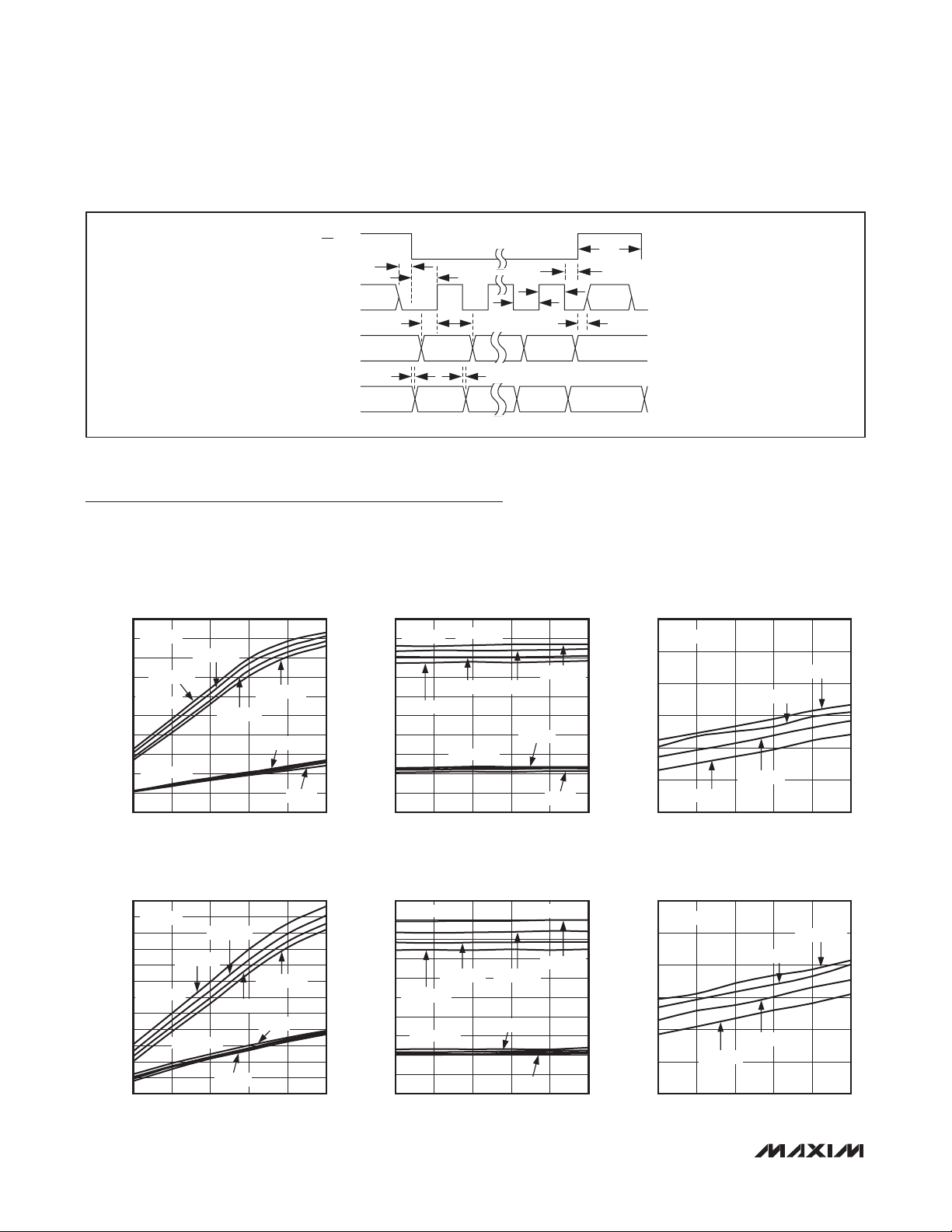
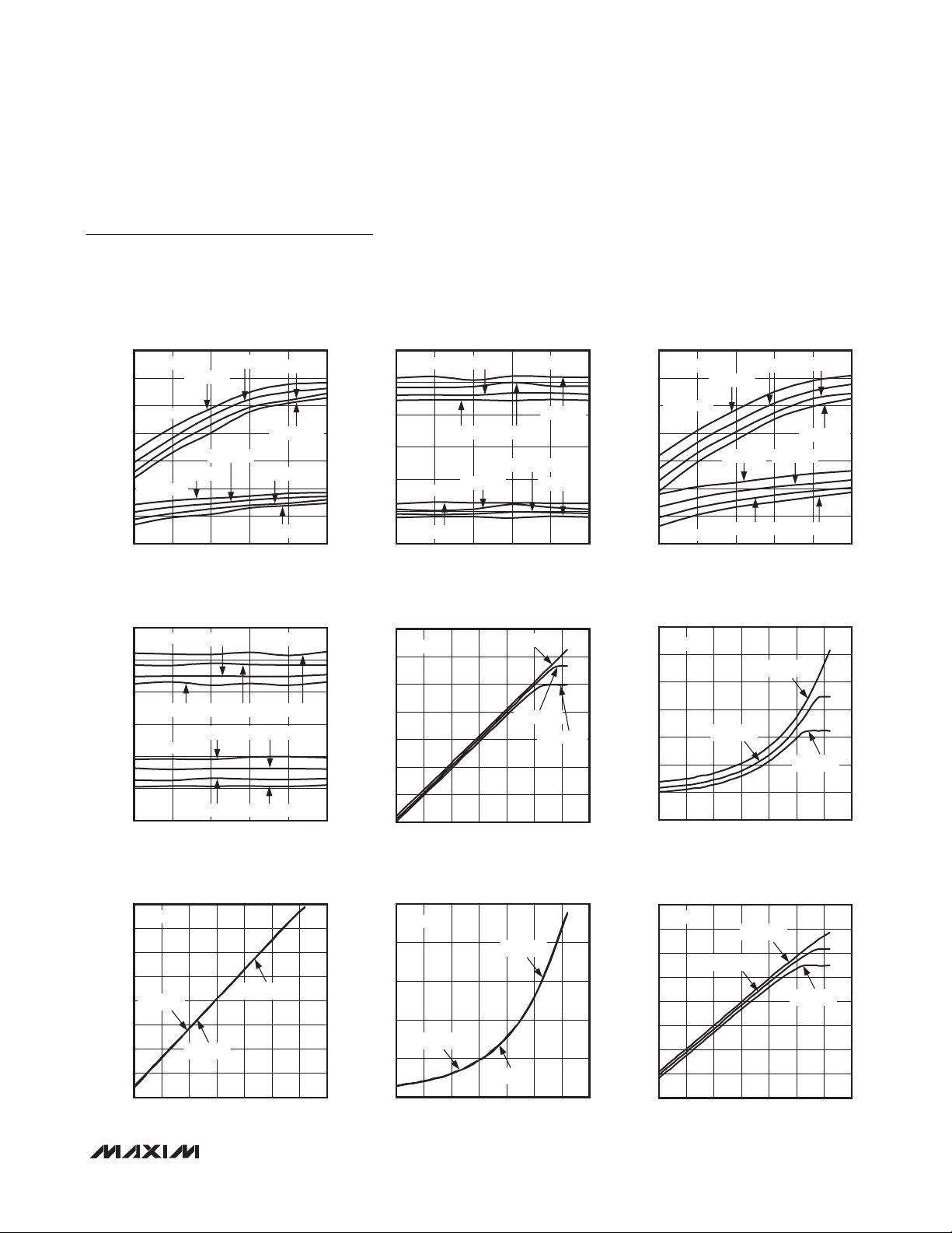
Typical Operating Characteristics
(Typical Application Circuit, 50I system impedance, V
450MHz, f
= V
PAVDD
= 16MHz, TA = -40NC to +125NC, unless otherwise noted. Typical values are at V
XTAL
= 2.7V, TA = +25NC, PA matched for optimum output power, unless otherwise noted. Supply current and output power are
greatly dependent on board layout and PAOUT match.)
SUPPLY CURRENT vs. SUPPLY VOLTAGE
(f
= 315MHz, PA ON)
30
28
26
24
22
20
18
16
SUPPLY CURRENT (mA)
14
12
10
RF
3V MODE
TA = -40°C
PApwr = 0x1E
PApwr = 0x16
TA = +25°C
TA = +85°C
V
DD5
TA = +125°C
+125°C
-40°C
3.33.02.72.42.1 3.6
(V)
30
28
MAX7060 toc01
26
24
22
20
18
16
SUPPLY CURRENT (mA)
14
12
10
DD5
= V
GPOVDD
= V
AVDD
= V
DVDD
SUPPLY CURRENT vs. SUPPLY VOLTAGE
= 315MHz, PA ON)
(f
RF
5V MODE
TA = +125°C
PApwr = 0x1E
TA = +85°C
PApwr = 0x16
V
TA = +25°C
(V)
DD5
TA = -40°C
+125°C
-40°C
5.35.14.94.74.5 5.5
= V
PAVDD =
8
MAX7060 toc02
7
6
5
4
SUPPLY CURRENT (mA)
3
2
2.1V to 3.6V, fRF = 280MHz to
DD5
= V
GPOVDD
= V
AVDD
SUPPLY CURRENT vs. SUPPLY VOLTAGE
(f
= 315MHz, PA OFF)
RF
3V MODE
TA = +125°C
TA = +85°C
TA = +25°C
TA = -40°C
3.33.02.72.42.1 3.6
V
(V)
DD5
= V
DVDD
MAX7060 toc03
SUPPLY CURRENT vs. SUPPLY VOLTAGE
(f
= 433.92MHz, PA ON)
38
36
34
32
30
28
26
24
22
SUPPLY CURRENT (mA)
20
18
16
14
RF
3V MODE
PApwr = 0x1E
2.1 3.6
TA = +25°C
TA = -40°C
PApwr = 0x16
TA = +85°C
+125°C
V
(V)
DD5
TA = +125°C
-40°C
MAX7060 toc04
3.33.02.72.4
SUPPLY CURRENT vs. SUPPLY VOLTAGE
= 433.92MHz, PA ON)
(f
36
34
32
30
28
26
24
22
SUPPLY CURRENT (mA)
20
18
16
RF
PApwr = 0x1E
TA = +125°C
PApwr = 0x16
TA = +25°CTA = +85°C
-40°C
+125°C
V
(V)
DD5
5V MODE
TA = -40°C
5.35.14.94.74.5 5.5
8
MAX7060 toc05
7
6
5
4
SUPPLY CURRENT (mA)
3
2
SUPPLY CURRENT vs. SUPPLY VOLTAGE
= 433.92MHz, PA OFF)
(f
RF
3V MODE
TA = -40°C
8 ______________________________________________________________________________________
TA = +85°C
TA = +25°C
V
(V)
DD5
TA = +125°C
3.33.02.72.42.1 3.6
MAX7060 toc06
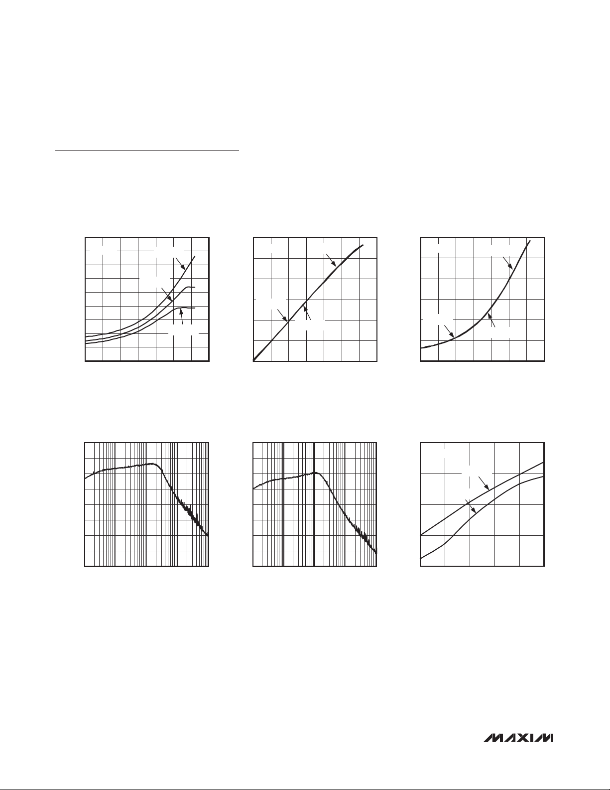
Page 9
280MHz to 450MHz Programmable
PA POWER
03
03
PA POWER
03
03
03
ASK/FSK Transmitter
Typical Operating Characteristics (continued)
(Typical Application Circuit, 50I system impedance, V
450MHz, f
= V
PAVDD
= 16MHz, TA = -40NC to +125NC, unless otherwise noted. Typical values are at V
XTAL
= 2.7V, TA = +25NC, PA matched for optimum output power, unless otherwise noted. Supply current and output power are
greatly dependent on board layout and PAOUT match.)
OUTPUT POWER vs. SUPPLY VOLTAGE
= 315MHz, PA ON)
(f
(dBm)
OUT
P
18
16
14
12
10
8
6
4
3V MODE
PApwr = 0x1E
PApwr = 0x16
RF
TA = -40°C
TA = -40°C
TA = +25°C
TA = +25°C
V
(V)
DD5
TA = +85°C
TA = +125°C
TA = +85°C
TA = +125°C
3.33.02.72.42.1 3.6
MAX7060 toc07
(dBm)
OUT
P
17
15
13
11
OUTPUT POWER vs. SUPPLY VOLTAGE
(f
= 433.92MHz, PA ON)
RF
PApwr = 0x1E
TA = +125°C
PApwr = 0x16
TA = +85°C
TA = +25°C
TA = -40°C
V
DD5
TA = +125°CTA = +25°C
(V)
5V MODE
TA = +85°C
TA = -40°C
5.35.14.94.74.5 5.5
MAX7060 toc10
(dBm)
OUT
P
20
15
10
-5
-10
-15
(dBm)
OUT
P
15
13
11
9
7
5
3
vs. PA POWER CODE, 315MHz
16
12
8
4
(dBm)
0
OUT
P
-4
-8
-12
-16
5V MODE
V
= 5.5V
DD5
V
= 5V
DD5
PA POWER CODE (DECIMAL)
V
= 4.5V
DD5
30255 10 15 20
5
30
MAX7060 toc13
25
20
15
SUPPLY CURRENT (mA)
10
DD5
= V
GPOVDD
= V
AVDD
OUTPUT POWER vs. SUPPLY VOLTAGE
= 315MHz, PA ON)
(f
RF
PApwr = 0x1E
9
PApwr = 0x16
7
5
TA = +125°C
TA = -40°C
TA = +85°C
TA = +25°C
V
DD5
5V MODE
TA = -40°C
TA = +25°C
TA = +85°C
TA = +125°C
(V)
PA POWER
vs. PA POWER CODE, 315MHz
V
= 3.6V
3V MODE
5
0
PA POWER CODE (DECIMAL)
DD5
V
DD5
= 2.7V
V
SUPPLY CURRENT
vs. PA POWER CODE, 315MHz
5V MODE
V
= 4.5V
DD5
V
= 5.5V
DD5
V
= 5V
DD5
5
PA POWER CODE (DECIMAL)
= V
DVDD
5.35.14.94.74.5 5.5
= 2.1V
DD5
30252015105
30252015105
= V
MAX7060 toc08
(dBm)
OUT
P
MAX7060 toc11
SUPPLY CURRENT (mA)
5
MAX7060 toc14
(dBm)
OUT
P
-10
-15
-20
5
PAVDD =
2.1V to 3.6V, fRF = 280MHz to
DD5
= V
GPOVDD
= V
AVDD
OUTPUT POWER vs. SUPPLY VOLTAGE
= 433.92MHz, PA ON)
(f
16
14
12
10
8
6
4
2
RF
3V MODE
PApwr = 0x1E
PApwr = 0x16
TA = -40°C
TA = -40°C
V
TA = +25°C
TA = +25°C
(V)
DD5
SUPPLY CURRENT
vs. PA POWER CODE, 315MHz
35
3V MODE
30
25
20
15
10
5
0
V
PA POWER CODE (DECIMAL)
DD5
= 2.7V
V
= 3.6V
DD5
vs. PA POWER CODE, 433.92MHz
20
3V MODE
15
10
5
0
-5
V
= 3.6V
DD5
V
= 2.7V
DD5
PA POWER CODE (DECIMAL)
= V
TA = +85°C
TA = +125°C
TA = +125°CTA = +85°C
3.33.02.72.42.1 3.6
V
= 2.1V
DD5
30252015105
V
= 2.1V
DD5
30255 10 15 20
DVDD
MAX7060
MAX7060 toc09
MAX7060 toc12
5
MAX7060 toc15
5
_______________________________________________________________________________________ 9
Page 10
280MHz to 450MHz Programmable
03
PA POWER
03
03
ASK/FSK Transmitter
Typical Operating Characteristics (continued)
(Typical Application Circuit, 50I system impedance, V
450MHz, f
= V
PAVDD
= 16MHz, TA = -40NC to +125NC, unless otherwise noted. Typical values are at V
XTAL
= 2.7V, TA = +25NC, PA matched for optimum output power, unless otherwise noted. Supply current and output power are
greatly dependent on board layout and PAOUT match.)
DD5
= V
GPOVDD
= V
AVDD
= V
DVDD
= V
PAVDD =
= V
DD5
2.1V to 3.6V, fRF = 280MHz to
GPOVDD
= V
AVDD
= V
DVDD
SUPPLY CURRENT
MAX7060
SUPPLY CURRENT (mA)
vs. PA POWER CODE, 433.92MH
45
3V MODE
40
35
30
25
20
15
10
5
0
PA POWER CODE (DECIMAL)
PHASE NOISE vs. OFFSET FREQUENCY
= 315MHz, TA = +25°C,
(f
RF
V
= 2.7V, PA CODE = 0x19)
-60
-70
-80
-90
-100
-110
PHASE NOISE (dBc/Hz)
-120
-130
-140
DD
1k 10M
OFFSET FREQUENCY (Hz)
SUPPLY CURRENT
Z
V
= 3.6V
DD5
V
= 2.7V
DD5
V
= 2.1V
DD5
MAX7060 toc16
(dBm)
P
302515 20105
5
vs. PA POWER CODE, 433.92MHz
15
5V MODE
10
5
0
V
= 5.5V
DD5
OUT
-5
-10
-15
V
DD5
PA POWER CODE (DECIMAL)
V
DD5
= 5V
= 4.5V
MAX7060 toc17
SUPPLY CURRENT (mA)
30252015105
5
vs. PA POWER CODE, 433.92MHZ
35
5V MODE
30
25
20
V
= 5.5V
15
DD5
10
5
PA POWER CODE (DECIMAL)
V
DD5
V
= 4.5V
DD5
= 5V
MAX7060 toc18
30252015105
5
PHASE NOISE vs. OFFSET FREQUENCY
= 433.92MHz, TA = +25°C,
(f
RF
V
= 2.7V, PA CODE = 0x19)
-50
-60
MAX7060 toc19
-70
-80
-90
-100
PHASE NOISE (dBc/Hz)
-110
-120
1M100k10k
-130
DD
1k 10M
OFFSET FREQUENCY (Hz)
1M100k10k
MAX7060 toc20
REFERENCE SPUR MAGNITUDE (dBc)
REFERENCE SPUR MAGNITUDE
vs. SUPPLY VOLTAGE
-40
3V MODE
-42
433.92MHz
315MHz
-44
-46
-48
2.1 3.6
SUPPLY VOLTAGE (V)
3.33.02.72.4
MAX7060 toc21
10 _____________________________________________________________________________________
Page 11

280MHz to 450MHz Programmable
ASK/FSK Transmitter
Typical Operating Characteristics (continued)
(Typical Application Circuit, 50I system impedance, V
450MHz, f
= V
PAVDD
= 16MHz, TA = -40NC to +125NC, unless otherwise noted. Typical values are at V
XTAL
= 2.7V, TA = +25NC, PA matched for optimum output power, unless otherwise noted. Supply current and output power are
greatly dependent on board layout and PAOUT match.)
REFERENCE SPUR MAGNITUDE
vs. SUPPLY VOLTAGE
-40
5V MODE
-42
-44
433.92MHz
315MHz
DD5
= V
MAX7060 toc22
GPOVDD
= V
AVDD
= V
DVDD
= V
PAVDD =
= V
DD5
2.1V to 3.6V, fRF = 280MHz to
GPOVDD
FSK SPECTRUM (fRF = 315MHz, +25°C, VDD = 2.7V,
PA CODE = 0x19 ±50kHz DEVIATION,
4kHz SQUARE WAVE ON DIN)
20
RBW = 10kHz
VBW = 10kHz
10
0
(dBm)
OUT
P
-10
= V
AVDD
MAX7060 toc23
= V
DVDD
MAX7060
-46
REFERENCE SPUR MAGNITUDE (dBc)
-48
4.5 5.5
SUPPLY VOLTAGE (V)
5.35.14.94.7
-20
-30
314.5 315.5
fRF (MHz)
315.3315.1314.9314.7
Pin Configuration/Functional Diagram
DD5
V
VOLTAGE
REGULATOR
PA POWER CONTROL
PA
ASK DATA
PULSE
SHAPING
5
EXPOSED PAD
GND
PAVOUT
12
ROUT
11
PAVDD
10
PAOUT
9
N.C.
8
LSHDN
7
FREQ2
CS_DEV
SDI_PWR1
SCLK_PWR0
ENABLE
N.C.
XTAL1
18 17 16 15 14 13
CRYSTAL OSCILLATOR
19
20
21
22
23
DIN
24
SERIAL
INTERFACE,
CONFIGURATION,
AND CONTROL
XTAL2
/K
AVDD
CHARGE
PUMP
PFD
FREQUENCY
DIVIDER
Σ∆
MODULATOR
LOOP
FILTER
VCO
MAX7060
3
N.C.
+
123456
GPO1
GPO2_MOD
DVDD
TQFN
GPOVDD
FREQ0
FREQ1
______________________________________________________________________________________ 11
Page 12
280MHz to 450MHz Programmable
ASK/FSK Transmitter
Pin Description
PIN NAME FUNCTION
(SPI Mode/Manual Mode) Digital Input/Output. GPO2 output in SPI mode. Acts as an SPI data
1 GPO2_MOD
2 GPO1
MAX7060
3 DVDD
4 GPOVDD
5 FREQ0
6 FREQ1
7 FREQ2
8 LSHDN
9, 15, 24 N.C. No Connection. Internally not connected. Leave unconnected.
10 PAOUT
11 PAVDD
12 ROUT
13 PAVOUT
14 V
16 AVDD
17 XTAL2 Crystal Input 2. XTAL2 can be driven from an AC-coupled external reference.
18 XTAL1 Crystal Input 1. AC-couple to GND if XTAL2 is driven from an AC-coupled external reference.
19
20 SDI_PWR1
21 SCLK_PWR0
22 ENABLE
23 DIN Transmit Data Digital Input. Internally pulled down.
— EP Exposed Pad. Solder evenly to the board’s ground plane for proper operation.
DD5
CS_DEV
output when CS_DEV is low. ASK (0)/FSK (1) modulation select input in manual mode. This pin is
internally pulled down in manual mode.
General-Purpose Output 1. In SPI mode, this pin can output many internal status signals. In
manual mode, this pin outputs the synthesizer lock-detect (lockdet) signal.
Digital-Supply Voltage Input. Bypass to GND with a 0.01FF capacitor as close as possible to the pin.
Power-Supply Voltage Input for GPOs and ESD-Protection Devices. Bypass to GND with a
0.01FF capacitor as close as possible to the pin.
Frequency-Select Pin 0 in Manual Mode. Internally pulled down. FREQ0 = FREQ1 = FREQ2 = 0
for SPI mode.
Frequency-Select Pin 1 in Manual Mode. Internally pulled down. FREQ0 = FREQ1 = FREQ2 = 0
for SPI mode.
Frequency-Select Pin 2 in Manual Mode. Internally pulled down. FREQ0 = FREQ1 = FREQ2 = 0
for SPI mode.
Low-Power Shutdown Current-Select Digital Input. Turns off internal POR circuit and disables
pullup/pulldown currents. Must be driven low for normal operation in 3V mode. Functional only in
3V mode. Connect to GND in 5V mode.
Power Amplifier Output. Requires a pullup inductor to PAVOUT, which can be part of the outputmatching network to an antenna.
Power Amplifier Predriver Power-Supply Input. Bypass to GND with a 680pF capacitor and a
0.01FF as close as possible to the pin.
Envelope-Shaping Resistor Connection. See the Typical Application Circuits and the ASK
Envelope Shaping sections for details.
Power Amplifier Power-Control Output. Controls the transmitted power. Connect to PA pullup
inductor. Bypass to ground with 680pF capacitor.
Supply Voltage Input. Bypass to ground with 0.01FF and 0.1FF capacitors.
Analog Supply Voltage and Regulator Output. Bypass to GND with 0.1FF and 0.01FF capacitors
as close as possible to the pin.
(SPI Mode/Manual Mode) Serial Peripheral Interface (SPI) Active-Low Chip-Select Input. FSK
frequency-deviation input (0 = low deviation, 1 = high deviation) in manual mode. Internally
pulled up.
(SPI Mode/Manual Mode) SPI Data Input in SPI Mode. Power-control MSB input in manual mode.
Internally pulled down.
(SPI Mode/Manual Mode) SPI Clock Input in SPI Mode. Power-control LSB input in manual
mode. Internally pulled down.
Enable Digital Input. All internal circuits (except the PA in ASK mode) are enabled on the rising
edge of ENABLE. Internally pulled down.
12 _____________________________________________________________________________________
Page 13

280MHz to 450MHz Programmable
Detailed Description
The MAX7060 is power and frequency programmable
from 280MHz to 450MHz. The MAX7060 has an internal
transmit power control that can be programmed over a
28dB power range. The MAX7060 has tuning capacitors
at the output of the power amplifier (PA) to ensure highpower efficiency at various programmable frequencies
with a single matching network.
The crystal-based architecture of the MAX7060 eliminates many of the common problems with SAW transmitters by providing greater modulation depth, faster
frequency settling, tighter tolerance of the transmit frequency, and reduced temperature dependence. In particular, the tighter transmit frequency tolerance means
that a superheterodyne receiver with a narrower IF
bandwidth (therefore lower noise bandwidth) can be
used. The payoff is better overall receiver performance
when using a superheterodyne receiver such as the
MAX1473, MAX1471, MAX7033, MAX7034, MAX7036,
and MAX7042.
The MAX7060 can be configured in either SPI or manual
mode, where the transmitter can easily be configured
without the need of an SPI interface.
In the 3V operation, the MAX7060 can be put in a lowpower shutdown mode by pulling ENABLE low and
LSHDN high. In this mode, all the blocks are shut down
including power-on reset (POR). All the MAX7060 registers must be reprogrammed after LSHDN is asserted
high. In the 5V operation, the low-power shutdown mode
is not available, and LSHDN should be connected to
GND.
Frequency Programming
The MAX7060 is a crystal-referenced phased-lockedloop (PLL) VHF/UHF transmitter that transmits data over
a wide frequency range. The internal VCO can be tuned
from 280MHz to 450MHz and controlled by a single
crystal to cover up to a 1.47:1 carrier-frequency range.
The transmit frequency is set by the crystal frequency
and the programmable divider in the PLL; the programmable PLL divide ratios can be set anywhere from 19 to
28, which means that with a crystal frequency of 15MHz,
the output is 285MHz to 420MHz. With a crystal frequency of 16MHz, the output is 304MHz to 448MHz.
The MAX7060 has an internal variable capacitor connected across the PA output. This capacitor can be programmed to maintain high-efficiency transmission at any
frequency within a 1.47 to 1 (28/19) tuning range. This
ASK/FSK Transmitter
means that it is possible to change the frequency and
retune the antenna to the new frequency in a very short
time. The combination of rapid antenna-tuning ability
with rapid synthesizer tuning makes the MAX7060 a true
frequency-agile transmitter. The tuning capacitor has a
nominal resolution of 0.25pF, from 0 to 7.75pF.
The MAX7060 supports data rates up to 100kbps NRZ
in ASK mode and 140kbps NRZ in FSK mode. In FSK
mode, the frequency deviation corresponding to bit 1
and bit 0 can be set as low as Q2kHz, and as high as
Q100kHz. The frequency deviation is fully programmable
in SPI mode, and can be selected either as Q16kHz or
Q50kHz in manual mode.
Power Amplifier (PA)
The PA of the MAX7060 is a high-efficiency, open-drain
switching-mode amplifier. In a switching-mode amplifier,
the gate of the final-stage FET is driven with a very sharp
25% duty-cycle square wave at the transmit frequency.
This square wave is derived from the synthesizer circuit.
When the matching network is tuned correctly, the output
FET resonates the attached tank circuit with a minimum
amount of power dissipated in the FET. With a proper
output-matching network, the PA can drive a wide range
of antenna impedances, which include a small-loop PCB
trace and a 50I antenna. The output-matching network
suppresses the carrier harmonics and transforms the
antenna impedance to an optimal impedance at PAOUT,
which is from 60I to 125I. When the output-matching
network is properly tuned, the MAX7060 transmits power
with a high overall efficiency. The efficiency of the PA
itself is approximately 50%.
Transmitter Power Control
The transmitter power of the MAX7060 can be set in
approximately 1dB steps (SPI mode) to produce a maximum output power level of +14dBm with a 5V supply.
If a battery is used as the supply, the maximum output
power level varies from +15dBm at 3.6V to +10dBm at
2.1V. The minimum power level is -14dBm for both 5V
and battery supplies. The maximum transmitter power
(and the transmitter current) can be lowered by increasing the load impedance on the PA. Four fixed power
levels are available in manual mode.
When a 5V supply is used, the V
are connected to the 5V supply. AVDD is the output of
an internal voltage regulator and must be connected
externally to DVDD and PAVDD. The PAVOUT pin is
connected to the PAOUT pin through a biasing inductor.
PAVOUT is not connected to any of the power-supply
and GPOVDD pins
DD5
MAX7060
______________________________________________________________________________________ 13
Page 14

280MHz to 450MHz Programmable
ASK/FSK Transmitter
pins. Connecting PAVOUT to PAOUT enables Tx power
control. In SPI mode, there are 31 power-control settings
in approximately 1dB monotonic steps. In manual mode,
four power-control settings are available.
ASK Envelope Shaping
The MAX7060 has two types of ASK envelope shaping:
digital shaping (SPI mode only) and analog shaping
through an internal resistor. Envelope shaping results
MAX7060
in a smaller spectral width of the modulated PA output
signal.
In digital shaping, the user can choose the final Tx power
setting, the power step size in units as small as 1dB, and
the step-time interval in units as small as 0.25Fs, when a
16MHz crystal is used. This shaping method causes the
PA to transmit an envelope that rises linearly in decibels
(exponentially in power) with time. Digital shaping is programmed through the SPI.
The analog shaping mode uses an internal envelopeshaping resistor for ASK modulation, which connects
between PAVOUT and ROUT. When the ROUT pin
(rather than the PAVOUT pin) is connected to the PA
pullup inductor, the envelope-shaping resistor slows the
turn-on/turn-off time of the PA. The user can choose two
turn-on/turn-off times through the SPI. A single turn-on/
turn-off time is set internally in manual mode.
It should be noted that, by default, data pulses applied
to the DIN pin are internally lengthened by 64 crystal
clock cycles (4μs for a 16MHz crystal) to allow time
for the analog shaping to occur. For cases in which
no analog shaping is desired, the PA pullup inductor
must be connected to PAVOUT and the analog shaping
bits in the Conf0 register set to either anshp[1:0] = 00,
which leaves the extra 4μs pulse extension in place, or
to anshp[1:0] = 11, which removes the extra 4μs and
allows transmitted pulses to track the data present at the
DIN pin. If digital shaping is used, the PA pullup inductor
must be connected to PAVOUT and there is no 4μs pulse
extension, regardless of the status of the anshp[1:0] bits.
At low data rates, where shaping is not necessary and
the 4μs pulse lengthening has minimal impact on duty
cycle symmetry, it may be acceptable to use the default
configuration of anshp[1:0] = 00. For higher data rates, it
may be necessary to use anshp[1:0] = 11, to avoid duty
cycle skew. Another method to remove the pulse lengthening is to apply a minimal amount of digital shaping,
by setting tstep[3:0] = 0001 and selecting pastep[4:0]
= papwr[4:0].
Variable Capacitor
The MAX7060 has an internal set of capacitors that can
be switched in and out to present different capacitor
values at the PA output. The capacitors are connected
from the PA output to ground. This allows changing the
tuning network along with the synthesizer divide ratio
each time the transmitted frequency changes, making
it possible to maintain maximum transmitter power while
moving rapidly from one frequency to another.
In SPI mode, the variable capacitor is programmed
through a register setting. In manual mode, the capacitor
setting is programmed through the DIN pin.
The tuning capacitor has a nominal resolution of 0.25pF,
from 0 to 7.75pF.
Phase-Locked Loop (PLL)
The MAX7060 utilizes a fully integrated fractional-N
PLL for its frequency synthesizer. All PLL components,
including the loop filter, are included on-chip. Two loop
bandwidths can be selected in SPI mode. The synthesizer has 16-bit fractional-N topology (4 bits integer, 12
bits fractional) with a divide ratio that can be set from 19
to 28, allowing the transmit frequency to be adjusted in
increments of f
The fractional-N architecture also allows exact FSK
frequency deviations to be programmed, completely
eliminating the problems associated with generating frequency deviations by crystal oscillator pulling.
FSK deviations as low as Q2kHz and as high as Q100kHz
can be set in SPI mode. In manual mode, the user can
select between Q16kHz and Q50kHz.
The integer and fractional portions of the PLL divider
ratio set the transmit frequency. This is done by loading the divide-ratio registers in SPI mode, or selecting
the states of the three frequency-control pins (FREQ2,
FREQ1, FREQ0) in manual mode. For ASK modulation,
the two 8-bit center-frequency registers (fce[15:0]) are
loaded with the divide ratio determined by the center
frequency and the crystal. For FSK modulation, the two
8-bit high (mark) frequency registers (fhi[15:0]) and the
two 8-bit low (space) frequency registers (flo[15:0]) are
loaded. The divide ratios for the fhi and flo are determined by the center frequency, the frequency deviation,
and the crystal frequency. Examples of typical settings
for ASK and FSK modulation are given in the SPI Mode
Settings section.
XTAL
/4096.
14 _____________________________________________________________________________________
Page 15

280MHz to 450MHz Programmable
11
= −×
++
Crystal (XTAL) Oscillator
The XTAL oscillator in the MAX7060 is designed to present a capacitance of approximately 6pF between the
XTAL1 and XTAL2 pins. In most cases, this corresponds
to a 8pF load capacitance applied to the external crystal
when typical PCB parasitics are added. It is very important to use a crystal with a load capacitance equal to the
capacitance of the MAX7060 crystal oscillator plus PCB
parasitics. If a crystal designed to oscillate with a different load capacitance is used, the crystal is pulled away
from its stated operating frequency, introducing an error
in the reference frequency. A crystal designed to operate at a higher load capacitance than the value specified
for the oscillator is always pulled higher in frequency.
Adding capacitance to increase the load capacitance
on the crystal increases the startup time and can prevent
oscillation altogether.
In actuality, the oscillator pulls every crystal. The crystal’s
natural frequency is really below its specified frequency,
but when loaded with the specified load capacitance,
the crystal is pulled and oscillates at its specified frequency. This pulling is already accounted for in the
specification of the load capacitance.
Additional pulling can be calculated if the electrical
parameters of the crystal are known. The frequency pulling is given by:
C
M
f 10
P
2CC CC
CASE LOAD CASE SPEC
where:
fP is the amount the crystal frequency pulled in ppm
CM is the motional capacitance of the crystal
C
C
C
When the crystal is loaded as specified (i.e., C
C
SPEC
is the case capacitance
CASE
is the specified load capacitance
SPEC
is the actual load capacitance
LOAD
), the frequency pulling equals zero.
LOAD
6
=
ASK/FSK Transmitter
MAX7060
General-Purpose Output
(GPO)/Clock Outputs
The MAX7060 has two GPO pins in SPI mode (GPO2_
MOD and GPO1) and one GPO in manual mode (GPO1).
The GPO1 pin can serve as a clock for a microprocessor
or any other GPO function in SPI mode. In manual mode,
this pin outputs the synthesizer lock-detect (lockdet)
status, after which the user can send data through the
DIN pin.
The GPO2_MOD pin acts as the SPI data output when
the CS_DEV pin is low, in SPI mode. When CS_DEV is
high, it acts as a GPO that can output various internal
signals, such as the synthesizer lock detect (lockdet).
In SPI mode, the output clock that can be routed through
GPO1 is a divided version of the crystal frequency. The
divide ratio is set through the MAX7060 registers, and
the divide settings are 1 (no division), 2, 4, 8, or 16.
When driving an output clock through GPO1, the gp1bst
bit (register Conf0, address 0x01, bit 6) can be set to
1 to increase GPO1 drive strength. If even more drive
capability is required, the user should provide an external buffer.
Serial Peripheral Interface (SPI)
The MAX7060 utilizes a 4-wire SPI protocol for programming its registers, configuring and controlling the
operation of the whole transmitter. For SPI operation, the
FREQ2, FREQ1, and FREQ0 pins must be reset to 0.
The following digital I/Os control the operation of the SPI:
CS_DEV Active-low SPI chip select
SDI_PWR1 SPI data Input
SCLK_PWR0 SPI clock
GPO2_MOD SPI data output
Figure 2 shows the general timing diagram of the SPI
protocol.
Any number of 8-bit data bursts (Data 1, Data 2 … Data
n) can be sent within one cycle of the CS_DEV pin, to
allow for burst-write or burst-read operations. The SPI
data output signal is routed through the GPO2_MOD pin
when CS_DEV is low.
______________________________________________________________________________________ 15
Page 16
280MHz to 450MHz Programmable
ASK/FSK Transmitter
CS_DEV
SCLK_PWR0
MAX7060
SDI_PWR1
DI7 DI6 DI5 DI4 DI3 DI2 DI1 DI0 DI7 DI6 DI5 DI4 DI3 DI2 DI1 DI0
GPO2_MOD
Figure 2. SPI Format
DO7 DO6 DO5 DO4 DO3 DO2 DO1 DO0 DO7 DO6 DO5 DO4 DO3 DO2 DO1 DO0
DATA 1 DATA n
SPI Commands
The following commands are implemented in the MAX7060:
Write: Within the same CS_DEV cycle, a write command is implemented as follows:
SDI_PWR1: <0x01> <Initial Address> <Data 1> <Data 2> … <Data N>
With this command, Data 1 is written to the address given by <Initial Address>, Data 2 is written to <Initial Address +
1>, and so on.
Read: Within the same CS_DEV cycle, a read command is implemented as follows:
SDI_PWR1: <0x02> <Address 1> <Address 2> <Address 3> … <Address N> <0x00>
GPO2_MOD: <0xXX> <0xXX> <Data 1> <Data 2> … <Data N - 1> <Data N>
With this command, all the registers can be read within the same cycle of CS_DEV. The addresses can be given in
any order.
CS_DEV
SCLK_PWR0
SDI_PWR1
WRITE COMMAND (0x01) INITIAL ADDRESS (A[7:0]) DATA 1
Figure 3. SPI Write Command Format
16 _____________________________________________________________________________________
A7 A6 A5 A4 A3 A2 A1 A0 D7 D6 D5 D4 D3
D2
D1 D0 D7 D0
DATA N
Page 17

CS_DEV
SCLK_PWR0
280MHz to 450MHz Programmable
ASK/FSK Transmitter
MAX7060
SDI_PWR1
READ COMMAND (0x02) ADDRESS 1 ADDRESS 2
GPO2_MOD
A7
A6 A5 A4 A3 A2 A1 A0 A7 A6 A5 A4 A3 A2 A1 A0 A7 A0
D7 D6 D5 D4 D3 D2 D1 D0 D7 D0 D0D7
DATA 1 DATA 2 DATA N
ADDRESS N 0x00
Figure 4. SPI Read Command Format
Read All: Within two CS_DEV cycles, the read-all command is implemented as follows:
CS_DEV Cycle 1 CS_DEV Cycle 2
SDI_PWR1: <0x03> <Address N> <0x00> <0x00> <0x00> ... <0x00>
GPO2_MOD: <Data N><Data N + 1><Data N + 2>...<Data N + n>
Reset: An SPI reset command is implemented as follows:
SDI_PWR1: <0x04>
An internal active-low master reset pulse is generated, from the falling edge of the last SCLK_PWR0 signal to the falling
edge of the following CS_DEV signal (t
CS_DEV
SCLK_PWR0
SDI_PWR1
READ-ALL COMMAND (0x03) ADDRESS N
GPO2_MOD
+ t
HCS
CSH
A7
A6 A5 A4 A3 A2 A1 A0
).
D7 D6 D5 D4 D3 D2 D1 D0 D7 D0 D0D7
DATA N
DATA N + 1
DATA N + n
Figure 5. SPI Read-All Command Format
CS_DEV
SCLK_PWRO
SDI_PWR1
INTERNAL
RESET PULSE
Figure 6. SPI Reset Command Format
______________________________________________________________________________________ 17
RESET COMMAND (0x04)
Page 18

280MHz to 450MHz Programmable
−× =
ASK/FSK Transmitter
Applications Information
SPI Mode Settings
ASK Carrier Frequency
When the MAX7060 is in ASK mode, only the carrier
frequency needs to be set. To do this, the user calculates the divide ratio based on the carrier frequency and
crystal frequency. The example below shows how to
MAX7060
determine the correct value to be loaded into the carrierfrequency registers (fce[15:0]).
Due to the nature of the transmit PLL frequency divider,
a fixed offset of 16 must be subtracted from the transmit PLL divider ratio for programming the MAX7060’s
transmit-frequency registers. To determine the value to
program the MAX7060’s transmit-frequency registers,
convert the decimal value of the following equation to the
nearest hexadecimal value:
f
RF
f
XTAL
Assume the ASK transmit frequency = 315MHz and
f
= 16MHz. In this example, the rounded decimal
XTAL
value is 15,104 or 0x3B00. The upper byte (0x3B) is
loaded into the FCenter0 register (fce[15:8]) and the
lower byte (0x00) is loaded into the FCenter1 register
(fce[7:0]).
16 4096
FSK Mark and Space Frequencies
When the MAX7060 is in FSK mode, two frequencies
need to be set: the mark (logical 1) frequency and the
space (logical 0) frequency. In most cases, the two frequencies are above and below the carrier frequency by
the deviation frequency. Therefore, the user needs to
calculate the divide ratio for both frequencies and load
them into four registers. The procedure for calculating
the register settings is the same as it is for calculating
the carrier frequency. The example below shows how to
determine the register settings for the mark and space
frequencies when the frequency deviation is ±50kHz
(100kHz between mark and space).
Assume that, for an FSK transmitter centered at
433.92MHz, the mark frequency is 433.97MHz, the
space frequency is 433.87MHz, and the crystal frequency is 16MHz. In this example, the rounded decimal
value for the mark frequency is 45,560 or 0xB1F8. For the
space frequency, the rounded decimal value is 45,535
or 0xB1DE. The mark setting is loaded into the FHigh0
and FHigh1 registers (fhi[15:0]), and the space setting
is loaded into the FLow0 and FLow1 registers (flo[15:0]).
decimal value to program the
transmit-frequency registers
Transmit Power Settings (5V Supply)
The output power level is set by entering a 5-bit value
into the PApwr register (papwr[4:0]). The highest setting
(30dec or 0x1E) corresponds to the highest transmitted power level. Each step is slightly less than 1dB
(approximately 0.95dB), with the lowest setting producing a transmitted power 28dB lower than the highest.
The highest transmitted power depends on the load
presented to the PA output. A 50I or 60I load produces
an output power level of +14dBm to +15dBm when the
highest papwr[4:0] setting (0x1E) is applied. Increasing
the load resistance reduces the output power level.
Reducing the setting by one step reduces the power by
approximately 1dB, and the minimum transmitted power
is still about 28dB below the maximum. For example, if
the load resistance is increased to the point where the
output power for the maximum setting (0x1E) is +10dBm,
then the minimum setting (0x00) produces an output
power of about -18dBm.
Transmit Power Settings (3V Supply)
The output power level in 3V operation is set the same
way as in 5V operation, but the variation in the 3V supply (the specified range is 2.1V to 3.6V) affects the
maximum power that can be transmitted. If the supply
is 3.6V, then the maximum papwr[4:0] setting (0x1E)
still produces a +14dBm to +15dBm transmitted power
level. As the supply voltage decreases, the transmitted
power at the highest settings is compressed, so that
the top setting and an increasing number of the lower
settings produce the same transmitted power, which
is lower than the +14dBm to +15dBm achieved with a
3.6V supply. For example, a 2.7V supply produces a
maximum transmitter power of +12dBm to +13dBm, and
the PApwr register settings from 0x1B to 0x1E (27dec to
30dec) produce the same transmitter power. Below this
compressed range, the power settings give the same
power levels that they would give with a 5V supply. At
the lowest supply level of 2.1V, the maximum setting
produces a maximum transmitter power of +10dBm, and
the PApwr register settings from 0x19 to 0x1E (25dec to
30dec) produce the same transmitter power. The effect
of a lower supply voltage reduces the maximum power
and the adjustment range. The power at the lowest setting remains unchanged.
The transmitted power using a 3V supply can be set
higher than the levels described in the paragraph above
by connecting PAOUT directly to PAVDD and disconnecting (leave open) the PAVOUT pin. The tradeoff of this
connection is that there is no transmit power adjustment.
18 _____________________________________________________________________________________
Page 19

280MHz to 450MHz Programmable
ASK Amplitude Shaping
At data rates higher than 30kbps Manchester (60kbps
NRZ), it may be necessary to shape the ASK transmitter
pulses to reduce the occupied bandwidth of the transmitted signal to comply with government regulations
(FCC in the U.S., ETSI in Europe). There is no shaping
of the FSK modulation. The MAX7060 has two forms of
amplitude shaping: digital and analog.
Digital Amplitude Shaping
The digital shaping feature allows the user to choose a
linear stairstep function to increase and decrease the
power when the PA is turned on and off for an ASK bit
interval. There are three registers that control the digital
amplitude shaping settings. The first setting is the final
power of the PA when the pulse reaches its maximum
(PApwr register). The second setting is the amplitude
change, in decibels, for each step, which is the vertical
axis of the stairstep (PAstep register). The third setting
is the time interval of each step, which is the horizontal
axis of the stairstep (Tstep register). The final power setting (decimal 0 to 30 in increments of 1dB) is entered in
the PApwr register. The amplitude step (decimal 0 to 30
in increments of 1dB) is entered in the PAstep register.
The time interval (decimal 0 to 60/f
4/f
shape an 80kbps NRZ data stream (12.5Fs bit interval),
the user might choose a maximum power level of 0x1E
(30dec), an amplitude step of 5dB, and a time interval
of 0.5Fs assuming a crystal frequency of 16MHz. This
would produce an ASK pulse that ramps up in 3Fs, levels off for 9.5Fs, and ramps down in 3Fs. Because the
amplitude steps are in decibels, the shape of the pulse
rise and fall is exponential on a linear display (an oscilloscope, for instance). Because most ASK receivers use
a logarithmic amplitude detector, the demodulated pulse
) is entered in the Tstep register. For example, to
XTAL
in increments of
XTAL
ASK/FSK Transmitter
MAX7060
has a linear ramp shape. The digital shaping is disabled
when the Tstep register is 0x00.
If no shaping of any kind is used (digital or analog), the
PA pullup inductor must be connected to PAVOUT and
the analog shaping bits in the Conf0 register must also
be set to either anshp[1:0] = 00 or to anshp[1:0] = 11, as
described in the ASK Envelope Shaping section.
Analog Amplitude Shaping
To use the analog shaping feature, the user must connect the bias inductor to the ROUT pin instead of directly
to the PAVOUT pin. This places a MOS resistor between
PAVOUT and ROUT, which slows down the application of
the PAVOUT voltage to the drain of the PA FET when the
PA is turned on. There are two settings in the anshp[1:0]
bits in the Conf0 register for the rate at which the pulse
ramps up: anshp[1:0] = 10 is approximately 1.5Fs and
anshp[1:0] = 01 is approximately 3Fs. The anshp[1:0] =
11 setting turns analog shaping off and removes the 4Fs
pulse extension, while the anshp[1:0] = 00 setting opens
the connection between PAVOUT and ROUT.
Tuning Capacitor Settings
The internal variable shunt capacitor, which can be used
to match the PA to the antenna with changing transmitter
frequency, is controlled by setting the 5-bit cap variable in the registers. This allows for 32 levels of shunt
capacitance control. Since the control of these 5 bits is
independent of the other settings, any capacitance value
can be chosen at any frequency, making it possible to
maintain maximum transmitter efficiency while moving
rapidly from one frequency to another. The internal tuning capacitor adds 0 to 7.75pF to the PA output in 0.25pF
steps. The PA output capacitance at the minimum cap
setting is approximately 4.5pF.
12.5µs 12.5µs
DIN
PApwr =
0x1E (30dec)
0
Tstep = 0x2 (0.5µs) Tstep = 0x2 (0.5µs)
Figure 7. Digital Amplitude Shaping Timing Diagram
______________________________________________________________________________________ 19
PAstep = 0x05 (5dB)
PAstep = 0x05 (5dB)
Page 20

280MHz to 450MHz Programmable
ASK/FSK Transmitter
Register Details
The following tables provide information on the MAX7060 registers.
Table 1. Register Summary
REGISTER ADDRESS DESCRIPTION
Ident 0x00 Read-only register used for identification purpose. The content of this register is always 0xA6.
MAX7060
Conf0 0x01
Conf1 0x02
Conf2 0x03 Configuration 2 register. Controls the emulation mode.
IOConf0 0x04 IO configuration 0 register. Selects the status register bus for SPI operation.
IOConf1 0x05 IO configuration 1 register. Selects the outputs of GPO1 and GPO2_MOD pins.
Tstep 0x06 Digital shaping time step register. Controls the time step in the digital shaping.
PAstep 0x07 Digital shaping power step register. Controls the power step in the digital shaping.
PApwr 0x08 Final power register. Controls the final output power.
FHigh0 0x09 High-frequency 0 register (upper byte). Sets the high frequency in FSK transmission.
FHigh1 0x0A High-frequency 1 register (lower byte). Sets the high frequency in FSK transmission.
FCenter0 0x0B Center-frequency 0 register (upper byte). Sets the carrier frequency in ASK transmission.
FCenter1 0x0C Center-frequency 1 register (lower byte). Sets the carrier frequency in ASK transmission.
FLow0 0x0D Low-frequency 0 register (upper byte). Sets the low frequency in FSK transmission.
FLow1 0x0E Low-frequency 1 register (lower byte). Sets the low frequency in FSK transmission.
FLoad 0x0F Frequency-load register. Performs the frequency-load function.
EnableReg 0x10 Enable register. Register equivalent of ENABLE pin.
DataReg 0x11 Datain register. Register equivalent of DIN pin.
Status 0x12 Status register
Configuration 0 register. Controls the GPO1 boost mode, PLL bandwidth, analog shaping, crystal clock output, and the modulation mode (ASK/FSK).
Configuration 1 register. Controls the clock output frequency divider and the capacitance at the
PA output.
Table 2. Configuration Registers
REGISTER ADDRESS
Ident 0x00 1 0 1 0 0 1 1 0 R
Conf0 0x01 — gp1bst pllbw anshp_1 anshp_0 clksby clkout mode R/W
Conf1 0x02 ckdiv_2 ckdiv_1 ckdiv_0 cap_4 cap_3 cap_2 cap_1 cap_0 R/W
Conf2 0x03 fixed fxmode fxpwr_1 fxpwr_0 fxhdev fxfrq_2 fxfrq_1 fxfrq_0 R/W
IOConf0 0x04 — — — — — tmux_2 tmux_1 tmux_0 R/W
IOConf1 0x05 — gp2s_2 gp2s_1 gp2s_0 — gp1s_2 gp1s_1 gp1s_0 R/W
Tstep 0x06 — — — — tstep_3 tstep_2 tstep_1 tstep_0 R/W
PAstep 0x07 — — — pastp_4 pastp_3 pastp_2 pastp_1 pastp_0 R/W
PApwr 0x08 — — — papwr_4 papwr_3 papwr_2 papwr_1 papwr_0 R/W
FHigh0 0x09 fhi_15 fhi_14 fhi_13 fhi_12 fhi_11 fhi_10 fhi_9 fhi_8 R/W
FHigh1 0x0A fhi_7 fhi_6 fhi_5 fhi_4 fhi_3 fhi_2 fhi_1 fhi_0 R/W
FCenter0 0x0B fce_15 fce_14 fce_13 fce_12 fce_11 fce_10 fce_9 fce_8 R/W
FCenter1 0x0C fce_7 fce_6 fce_5 fce_4 fce_3 fce_2 fce_1 fce_0 R/W
20 _____________________________________________________________________________________
BIT 7 BIT 6 BIT 5 BIT 4 BIT 3 BIT 2 BIT 1 BIT 0 MODE
DATA
Page 21

280MHz to 450MHz Programmable
ASK/FSK Transmitter
Table 2. Configuration Registers (continued)
REGISTER ADDRESS
FLow0 0x0D flo_15 flo_14 flo_13 flo_12 flo_11 flo_10 flo_9 flo_8 R/W
FLow1 0x0E flo_7 flo_6 flo_5 flo_4 flo_3 flo_2 flo_1 flo_0 R/W
FLoad 0x0F — — — — — — — hop R/W
EnableReg 0x10 — — — — — — — enable R/W
DataReg 0x11 — — — — — — — datain R/W
Status 0x12 status_7 status_6 status_5 status_4 status_3 status_2 status_1 status_0 R
BIT 7 BIT 6 BIT 5 BIT 4 BIT 3 BIT 2 BIT 1 BIT 0 MODE
Table 3. Identification (Ident) Register (Address: 0x00)
BIT NAME FUNCTION
7:0 ident Read-only register used for identification purpose. The content of this register is always 0xA6.
Table 4. Configuration 0 (Conf0) Register (Address: 0x01)
BIT NAME FUNCTION
6 gp1bst
5 pllbw
4:3 anshp[1:0]
2 clksby Crystal clock output enable (1) while part is in standby mode
1 clkout Crystal clock output enable (1) on GPO1 output, gp1s[2:0] = 0x2
0 mode ASK (0) or FSK (1)
0 = Normal GPO1 output driver
1 = Extended driving capability on GPO1
PLL bandwidth setting, low (0) = 300kHz or high (1) = 600kHz; 300kHz is recommended for fractional-N
and 600kHz for fixed-N (ASK mode only)
Control time constants of the analog shaping (bias inductor connected to the ROUT pin)
anshp[1:0] Rise/fall time
00 ROUT open-circuited, 4Fs pulse extension present
01 nominal 3.0Fs rise/fall time
10 nominal 1.5Fs rise/fall time
11 no analog shaping, no 4Fs pulse extension
DATA
MAX7060
Table 5. Configuration 1 (Conf1) Register
(Address: 0x02)
BIT NAME FUNCTION
7:5 ckdiv[2:0] 3-bit clock output frequency divider
4:0 cap[4:0] 5-bit capacitor setting
______________________________________________________________________________________ 21
Table 6. Crystal Divide Settings for Clock
Output
ckdiv[2:0]
000 1
001 2
010 4
011 8
1XX 16
CRYSTAL FREQUENCY
DIVIDED BY
Page 22

280MHz to 450MHz Programmable
ASK/FSK Transmitter
Table 7. Configuration 2 (Conf2) Register (Address: 0x03)
BIT NAME FUNCTION
7 fixed Enable (1) or disable (0) emulation mode
6 fxmode FSK (1) or ASK (0)
Output power setting
5:4 fxpwr[1:0]
MAX7060
3 fxhdev 100kHz (1) or 32kHz (0) frequency deviation in FSK
2:0 fxfrq[2:0]
fxpwr[1:0] dB below P
00 0
01 3
10 6
11 10
Frequency selection
The combinations are same as those in manual mode. When a 16MHz crystal is used, the following frequency values are selected by fxfrq[2:0].
fxfrq[2:0] Freq (MHz) Divide Ratio
000 N/A N/A
001 315.00 19.68750
010 433.62 27.10125
011 390.00 24.37500
100 418.00 26.12500
101 372.00 23.25000
110 345.00 21.56250
111 433.92 27.12000
MAX
Table 8. IO Configuration 0 (IOConf0) Register (Address: 0x04)
BIT NAME FUNCTION
2:0 tmux[2:0] Status register output selection bits
22 _____________________________________________________________________________________
Page 23

280MHz to 450MHz Programmable
ASK/FSK Transmitter
Table 9. IO Configuration 1 (IOConf1) Register (Address: 0x05)
BIT NAME FUNCTION
GPO2 output selection
CS_DEV Bit 2 Bit 1 Bit 0 GPO2_MOD
0 X X X SPI Data Output
1 0 0 0 lockdet
1 0 0 1 —
6:4 gp2s[2:0]
2:0 gp1s[2:0]
1 0 1 0 ckout
1 0 1 1 —
1 1 0 0 —
1 1 0 1 nock
1 1 1 0 —
1 1 1 1 —
GPO1 output selection
Bit 2 Bit 1 Bit 0 GPO1
0 0 0 lockdet
0 0 1 —
0 1 0 ckout
0 1 1 —
1 0 0 —
1 0 1 nock
1 1 0 —
1 1 1 —
MAX7060
where:
— Reserved signals
nock No-clock flag (1) if crystal oscillator is disabled, and (0) if clock activity is observed
ckout Clock output signal, according to programmed dividers (ckdiv[2:0])
lockdet PLL lock-detect flag
Table 10. ASK Digital Shaping Time Step (Tstep) Register (Address: 0x06)
BIT NAME FUNCTION
3:0 tstep[3:0] Time interval value used in digital shaping, in increments of 4/f
XTAL
Table 11. PA Digital Shaping Amplitude Step (PAstep) Register (Address: 0x07)
BIT NAME FUNCTION
4:0 pastp[4:0] Power step in digital shaping, in increments of 1dB
Table 12. PA Power (PApwr) Register (Address: 0x08)
BIT NAME FUNCTION
4:0 papwr[4:0] Final PA output power setting
Table 13. FSK High-Frequency 0 (FHigh0) Register (Address: 0x09)
BIT NAME FUNCTION
7:0 fhi[15:8] 8-bit upper byte of high-frequency divider for FSK
______________________________________________________________________________________ 23
Page 24

280MHz to 450MHz Programmable
ASK/FSK Transmitter
Table 14. FSK High-Frequency 1 (FHigh1) Register (Address: 0x0A)
BIT NAME FUNCTION
7:0 fhi[7:0] 8-bit lower byte of high-frequency divider for FSK
The 4 MSBs of FHigh0, fhi[15:12], are the integer portion of the divider, excluding offset of 16. The 12 LSBs (fhi[11:0])
are the fractional part of the divider.
MAX7060
Table 15. ASK Center-Frequency 0 (FCenter0) Register (Address: 0x0B)
BIT NAME FUNCTION
7:0 fce[15:8] 8-bit upper byte of frequency divider for ASK
Table 16. ASK Center-Frequency 1 (FCenter1) Register (Address: 0x0C)
BIT NAME FUNCTION
7:0 fce[7:0] 8-bit lower byte of frequency divider for ASK
The 4 MSBs of FCenter0, fce[15:12], are the integer portion of the divider, excluding offset of 16. The 12 LSBs (fce[11:0)
are the fractional part of the divider.
When fce[11:0] are all zeros and ASK mode is selected (mode bit = 0), the PLL works in the fixed-N mode, which
reduces current consumption and reference spurs. Set pllbw bit high (Conf0 register, bit 5). For all other combinations,
the PLL works in fractional-N mode.
Table 17. FSK Low-Frequency 0 (FLow0) Register (Address:0x0D)
BIT NAME FUNCTION
7:0 flo[15:8] 8-bit upper byte of low-frequency divider for FSK
Table 18. FSK Low-Frequency 1 (FLow1) Register (Address: 0x0E)
BIT NAME FUNCTION
7:0 flo[7:0] 8-bit lower byte of low-frequency divider for FSK
The 4 MSBs of FLow0, flo[15:12], are the integer portion of the divider, excluding offset of 16. The 12 LSBs (flo[11:0])
are the fractional part of the divider.
Table 19. Maximum and Minimum Values for Frequency Divider
DECIMAL VALUE fhi[15:0], fce[15:0], flo[15:0]
12.0220 0xC05A
2.9536 0x2F42
Table 20. Frequency-Load (FLoad) Register (Address: 0x0F)
BIT NAME FUNCTION
0 hop
Effectively changes the PLL frequency to the ones written in registers 0x09 to 0x0E. This is a self-reset bit
and is reset to zero after the operation is completed.
24 _____________________________________________________________________________________
Page 25

280MHz to 450MHz Programmable
ASK/FSK Transmitter
Table 21. Enable (EnableReg) Register (Address: 0x10)
BIT NAME FUNCTION
0 enable
Table 22. Data Input (DataReg) Register (Address: 0x11)
BIT NAME FUNCTION
0 datain
Table 23. Status (Status) Register (Address: 0x12)
BIT NAME FUNCTION
7:0 status[7:0] Read-only status register, selected through tmux[2:0] (register 0x04 IOConf0)
Table 24. Status Bus Signals
tmux[2:0] status[7] status[6] status[5] status[4] status[3] status[2] status[1] status[0]
0 — — — — ckout ckd16 ckd4 nock
1 — — — — — — — —
2 — — — — enable — — —
3 — frac_fxdb — cap[4] cap[3] cap[2] cap[1] cap[0]
4 — — notover capfxd[4] capfxd[3] capfxd[2] capfxd[1] capfxd[0]
5 integ[3] integ[2] integ[1] integ[0] frac[11] frac[10] frac[9] frac[8]
6 frac[7] frac[6] frac[5] frac[4] frac[3] frac[2] frac[1] frac[0]
7 — — — — — — lockdet xmit_en
SPI equivalent of the ENABLE pin, which should be kept low (0) if the external ENABLE pin is used. The
external ENABLE pin should also be kept low (0) if the enable bit is used.
SPI equivalent of DIN, where the transmitted data can be controlled through the SPI interface. It should
be kept low (0) if only the external DIN pin is used. The external DIN pin should also be kept low (0) if the
datain bit is used.
MAX7060
— Reserved signals
nock No-clock flag (1) if crystal oscillator is dis-
abled, and (0) ic clock activity is observed
ckd4 Crystal clock signal divided by 4
ckd16 Crystal clock signal divided by 16
ckout Clock output signal, according to pro-
grammed dividers (ckdiv[2:0])
enable Internal enable signal (OR function of the
ENABLE pin and enable bit)
cap[4:0] SPI mode capacitor setting
______________________________________________________________________________________ 25
frac_fxdb Fractional-N mode (1) or ASK fixed-N mode
(0)
capfxd[4:0] Emulation mode variable capacitor setting
notover ASK digital shaping flag (1) when PA power
value is different than 0
integ[3:0] Fractional-N 4-bit integer value
frac[11:0] Fractional-N 12-bit fractional value
xmit_en Transmitter PA enable flag
lockdet PLL lock-detect flag
Page 26

280MHz to 450MHz Programmable
ASK/FSK Transmitter
Manual Mode Settings
The MAX7060 can be operated by controlling certain
pins directly, thereby eliminating the need for an SPI
controller. There is a restricted selection of frequency
and power settings, but operation is simpler. The pins
that are used in manual mode are as follows:
Pin 1: GPO2_MOD (modulation mode, 0 = ASK,
MAX7060
Pins 5, 6, 7: FREQ0, FREQ1, FREQ2
Pin 19: CS_DEV (FSK deviation selection, 0 = Q16kHz,
Pins 20, 21: SDI_PWR1 and SCLK_PWR0 (2-pin power
Pins 22, 23: ENABLE and DIN (PA variable capacitor
setting, data input, enable)
To put the MAX7060 in manual mode, set any of the
FREQ0, FREQ1, FREQ2 pins (5, 6, and 7) to logic-high.
These pins are normally pulled down, so the default
state of the MAX7060 is for SPI operation. The settings in
Table 25 can be made in manual mode.
1 = FSK)
1 = Q50kHz)
selection)
Table 25. Manual Mode Frequency Selection
FREQ2 FREQ1 FREQ0 FREQUENCY (MHz) DIVIDE RATIO
0 0 0 SPI N/A
0 0 1 315.00 19.68750
0 1 0 433.62 27.10125
0 1 1 390.00 24.37500
1 0 0 418.00 26.12500
1 0 1 372.00 23.25000
1 1 0 345.00 21.56250
1 1 1 433.92 27.12000
Frequency Selection
There are seven internally set fractional-N divide ratios
that correspond to commonly used frequencies when a
16MHz crystal is used.
Notice that the MAX7060 can be operated manually at
any single frequency over its 280MHz to 450MHz operating range by choosing a crystal frequency and one of the
divide ratios from Table 25. For example, a transmitting
frequency of 308MHz can be achieved by selecting the
19.68750 divide ratio and a 15.6444MHz crystal.
The frequency settings in the manual mode of operation were designed in a way that allows the customer to
toggle only one control line between low and high states
to switch between seven commonly used frequency
pairs (see Table 26).
ASK or FSK Modulation
Reset pin 1 (GPO2_MOD) to 0 for ASK modulation and
1 for FSK modulation. Analog shaping in ASK mode is
enabled by using the ROUT pin. The turn-on and turn-off
time is fixed at approximately 1μs.
Table 26. Manual Mode Frequency Pair Switching
LOW FREQUENCY
(MHz)
315.00 433.92 001 to 111. Set FREQ0 high, shorting FREQ1 and FREQ2, toggling 1 line.
418.00 433.92 100 to 111. Set FREQ2 high, shorting FREQ1 and FREQ0, toggling 1 line.
433.62 433.92 010 to 111. Set FREQ1 high, shorting FREQ2 and FREQ0, toggling 1 line.
315.00 390.00 001 to 011. Set FREQ0 high and FREQ2 low, toggling FREQ1.
315.00 372.00 001 to 101. Set FREQ1 low and FREQ0 high, toggling pin FREQ2.
345.00 433.92 110 to 111. Set FREQ2 and FREQ1 high, toggling FREQ0.
390.00 433.92 011 to 111. Set FREQ1 and FREQ0 high, toggling FREQ2.
26 _____________________________________________________________________________________
HIGH FREQUENCY
(MHz)
FREQ2, FREQ1, FREQ0
Page 27

280MHz to 450MHz Programmable
Table 27. Output Power Settings
SDI_PWR1 SCLK_PWR0
0 0 0
0 1 3
1 0 6
1 1 10
Frequency Deviation
Reset pin 19 (CS_DEV) to 0 for 32kHz (Q16kHz) FSK
deviation and 1 for 100kHz (Q50kHz) FSK deviation.
Transmitter Power
Set SDI_PWR1 (pin 20) and SCLK_PWR0 (pin 21) to four
power settings (relative to the maximum power setting).
Note that at battery voltages below 3V, the top two power
settings are compressed and the power difference is
less than 3dB.
PA Variable Capacitor Setting
In manual mode, capacitance can be added to the PA
output for one selected frequency. This allows the user
to adjust the matching network when switching between
two frequencies in the manual selection table, or for
switching to one frequency that is significantly different
from the others in the table. The user can set the capacitance by resetting the ENABLE pin to a logic-low, then
selecting the frequency for which the variable capacitor
is to be added from the seven possible settings, and
then sending a stream of 1 to 32 pulses through the DIN
pin. The first pulse is used to reset the internal capacitor
counter and to latch the selected frequency. After the first
pulse, the remaining number of pulses sent equals the
variable capacitor setting. When the ENABLE pin goes
high, the capacitor setting for the specified frequency is
set, so that it adds the programmed capacitance to the
PA when the chosen frequency is selected. This scheme
must be executed only once to set the value of the variable capacitor.
For example, a user can operate the MAX7060 at
315MHz and 433.92MHz into a narrowband antenna
by resetting the ENABLE pin low, setting the FREQ0,
FREQ1, FREQ2 pins to 001 (315MHz), and sending the
appropriate number of pulses into the DIN pin, and then
setting the ENABLE pin high. When the frequency is set
to 433.92MHz (or any other frequency in the table except
315MHz), no capacitance is added to the PA output.
dB BELOW
P
MAX
ASK/FSK Transmitter
MAX7060
When the frequency is set to 315MHz, the PA capacitance increases by the programmed value.
Figure 8 illustrates how to set the capacitance. It begins
with the ENABLE pin pulled low. The frequency is
sampled at the rising edge of the first pulse. Pulses
2–11 set the capacitance code to 0x0A (10dec), which
is approximately 2.5pF. The ENABLE pin is then pulled
high to finish the setting.
Emulation Mode Settings
All the settings available through the manual mode of
operation are also easily accessible in the SPI mode.
This mode is called emulation mode, whereby only writing one or two registers, the whole transmitter can be
configured. The Conf2 register controls this mode.
The emulation mode is a subset of SPI mode. It gives SPI
users the capability to operate the part by programming
just one or two registers instead of all registers.
Since it is still SPI mode, pins 5, 6, and 7 (FREQ0, FREQ1,
and FREQ2) must be pulled low. The Conf2 register is
the only register that needs to be programmed. Setting
bit 7 (fixed) to 1 enables this mode. Bit 6 (fxmode) is
equivalent to pin 1 (GPO2_MOD) in manual mode. Bits
5 and 4 (fxpwr[1:0]) are equivalent to pin 20 and 21
(SDI_PWR1 and SCLK_PWR0) in manual mode. Bit 3
(fxhdev) is equivalent to pin 19 (CS_DEV) in manual
mode. Bits 2, 1, and 0 (fxfrq[2:0]) are equivalent to pins
5, 6, and 7 (FREQ0, FREQ1, and FREQ2) in manual
mode.
Similar to manual mode, the PA capacitor setting in the
emulation mode can be done by toggling the DIN pin
with the ENABLE pin low. In addition, the capacitor setting can also be done by directly writing to the capacitor
register (bits 4:0 of the Conf1 register, cap[4:0]). As long
as the capacitor register value is not zero, the capacitor
value sent in by toggling the DIN pin is ignored.
Control Interface Considerations
When operating the MAX7060 with a +4.5V to +5.5V
supply voltage, the CS_DEV, SCLK_PWR0, SDI_PWR1,
FREQ0, FREQ1, FREQ2, ENABLE, DIN, and LSHDN
pins can be driven by a microcontroller with either 3V or
5V interface logic levels. When operating the MAX7060
with a +2.1V to +3.6V supply, the microcontroller must
produce logic levels that conform to the VIH and VIL
specifications in the DC Electrical Characteristics for the
MAX7060.
______________________________________________________________________________________ 27
Page 28

280MHz to 450MHz Programmable
ASK/FSK Transmitter
ENABLE
FREQ[2:0]
MAX7060
CAPTURED
CAP VALUE
X 0x1
DIN
CAP CODE
X 0x0A
Figure 8. Variable Capacitor Setting Timing Diagram
Typical Application Circuits
SPI Mode (5V Supply)
Y1
DIGITAL
CONTROLLER
C1 C4 +3V
C2 C3 C5
XTAL1
19
CS_DEV
20
SDI_PWR1
21
SCLK_PWR0
22
ENABLE
23
DIN
24
N.C.
GPO2_MOD GPO1 DVDD GPOVDD FREQ0
XTAL2 AVDD
12
+3V
REG
161718
MAX7060
EXPOSED PAD
34 56
REG
C12
C11
+5V
C6
15
14
N.C.
V
DD5
C7 C8
13
PAVOUT
ROUT
PAVDD
PAOUT
N.C.
LSHDN
FREQ2
FREQ1
12
+3V
11
C9
10
9
8
7
REG
C10
L1
Tx
ANTENNA
MATCHING
NETWORK
COMPONENTS
+5V
28 _____________________________________________________________________________________
Page 29

280MHz to 450MHz Programmable
ASK/FSK Transmitter
Typical Application Circuits (continued)
Manual Mode (3V Supply, Shaped ASK Modulation, 315MHz)
MAX7060
C1 C4 +3V
19
20
21
Y1
C2 C3
XTAL1
CS_DEV
SDI_PWR1
SCLK_PWR0
XTAL2 AVDD
C5
151618 17
N.C.
+3V
C6 C7
14
V
DD5
13
PAVOUT
ROUT
PAVDD
12
+3V
11
C9
C10
C8
L1
Tx
ANTENNA
MAX7060
DIGITAL
CONTROLLER
22
ENABLE
23
DIN
24
N.C.
GPO2_MOD GPO1 DVDD GPOVDD FREQ0
12
EXPOSED PAD
34 56
C12
+3V
C11
FREQ1
PAOUT
N.C.
LSHDN
FREQ2
10
9
8
7
MATCHING
NETWORK
COMPONENTS
Component List
DESIGNATION QTY DESCRIPTION
C1, C4 2 May not be needed for low C
C2, C3 2
C5, C6 2
C7, C8, C9 3
C10, C11, C12 3
L1 1
Matching Network
Components
1.5nF ±10%, 50V X7R ceramic capacitors (0603)
Murata GRM188R71H152K
100nF ±10%, 50V X7R ceramic capacitors (0603)
Murata GRM188R71H104K
220pF ±5% ceramic capacitors (0603)
Murata GRM1885C1H220JA01D
10nF ±10%, 50V X7R ceramic capacitors (0603)
Murata GRM188R71H103K
±5% wire-wound inductor (0603)
Murata LQW18 series (value depends on matching network)
4 3 capacitors and 1 inductor (values depend on frequency range and antenna impedance)
crystals, depending on PCB layout parasitics
LOAD
U1 1 Maxim MAX7060ATG+
Y1 1
16MHz crystal, 10pF C
Crystek 17466
LOAD
Suntsu SCX284
______________________________________________________________________________________ 29
Page 30

280MHz to 450MHz Programmable
ASK/FSK Transmitter
Chip Information
PROCESS: CMOS
MAX7060
Package Information
For the latest package outline information and land patterns
(footprints), go to www.maxim-ic.com/packages. Note that a
“+”, “#”, or “-” in the package code indicates RoHS status only.
Package drawings may show a different suffix character, but
the drawing pertains to the package regardless of RoHS status.
PACKAGE
TYPE
24 TQFN-EP T2444+3
PACKAGE
CODE
OUTLINE
NO.
21-0139 90-0021
LAND
PATTERN NO.
30 _____________________________________________________________________________________
Page 31

280MHz to 450MHz Programmable
ASK/FSK Transmitter
Revision History
MAX7060
REVISION
NUMBER
0 2/10 Initial release —
1 2/12
REVISION
DATE
DESCRIPTION
Power dissipation and derating factor shown for wrong package type;
clarified GPO1 boost mode and nature of analog and digital ASK envelope
shaping. Added paragraph on control interface considerations; updated
Typical Application Circuits to add exposed pad (grounded); and specified
typical load C on crystal in component list
PAGES
CHANGED
2, 14, 15, 19, 21, 27,
28, 29
Maxim cannot assume responsibility for use of any circuitry other than circuitry entirely embodied in a Maxim product. No circuit patent licenses are implied.
Maxim reserves the right to change the circuitry and specifications without notice at any time. The parametric values (min and max limits) shown in the Electrical
Characteristics table are guaranteed. Other parametric values quoted in this data sheet are provided for guidance.
Maxim Integrated Products, 120 San Gabriel Drive, Sunnyvale, CA 94086 408-737-7600 31
©
2012 Maxim Integrated Products Maxim is a registered trademark of Maxim Integrated Products, Inc.
 Loading...