

Page 1

E V A L U A T I O N K IT A V A I L A B L E
19-5867; Rev 0; 6/11
MAX7049
High-Performance, 288MHz to 945MHz
ASK/FSK ISM Transmitter
General Description
The MAX7049 high-performance, single-chip, ultralow-power ASK/FSK UHF transmitter operates in the
industrial, scientific, medical (ISM) band at 288MHz to
945MHz carrier frequencies. The IC also includes a low
phase noise fractional-N synthesizer for precise tuning,
fast frequency agility, and low out-of-band power. To
support narrow-band applications, the IC has both
amplitude-shaping and frequency-shaping functions that
enable the user to optimize spectral efficiency. The IC
offers Tx power up to +15dBm. These features make the
transmitter ideally suited for long-range applications.
Additional system-level features of the IC include a digital
temperature sensor and a number of flexible GPOs for
monitoring radio status and for the control of external
functions. A complete transmitter system can be built
using a low-end microprocessor control unit (MCU), the
IC, a crystal, and a small number of passive components.
The IC is available in a small, 5mm x 5mm, 28-pin TQFN
package with an exposed pad. It is specified to operate
in the -40°C to +125°C automotive temperature range.
Applications
Automatic Meter Reading (AMR)
RF Modules
Long-Range, One-Way Remote Keyless Entry (RKE)
Wireless Sensor Networks
TPMS
Home Security
Home Automation
RFID
Remote Controls
Benefits and Features
S Transmitter (Tx)
Provides Long Transmit Range Up to +15dBm
21mA Tx Current for +10dBm Tx Power*
41mA Tx Current for +15dBm Tx Power*
Modulation Shaping, ASK, FSK
S General
Delivers Long Battery Life
< 50nA Shutdown Current
< 350nA Sleep Current
Minimizes the Number of I/Os Required
Between the IC and the MCU Serial Peripheral
Interface (SPI™)
Regulatory Compliant
FCC Part 15 Frequency Hopping
ETSI EN300-220 Compatible
On-Chip Temperature Sensor
Fast Fractional-N Synthesizer with a
User-Defined External Loop Filter
*VDD = 3.0V. Includes losses for the matching network and
regulatory-compliant harmonic filter.
Ordering Information appears at end of data sheet.
For related parts and recommended products to use with this part,
refer to www.maxim-ic.com/MAX7049.related.
SPI is a trademark of Motorola, Inc.
����������������������������������������������������������������� Maxim Integrated Products 1
For pricing, delivery, and ordering information, please contact Maxim Direct at 1-888-629-4642,
or visit Maxim’s website at www.maxim-ic.com.
Page 2

MAX7049
High-Performance, 288MHz to 945MHz
ASK/FSK ISM Transmitter
TABLE OF CONTENTS
Absolute Maximum Ratings . . . . . . . . . . . . . . . . . . . . . . . . . . . . . . . . . . . . . . . . . . . . . . . . . . . . . . . . . . . . . . . . . . . . . . 5
DC Electrical Characteristics . . . . . . . . . . . . . . . . . . . . . . . . . . . . . . . . . . . . . . . . . . . . . . . . . . . . . . . . . . . . . . . . . . . . . 5
AC Electrical Characteristics . . . . . . . . . . . . . . . . . . . . . . . . . . . . . . . . . . . . . . . . . . . . . . . . . . . . . . . . . . . . . . . . . . . . . 6
Typical Operating Characteristics . . . . . . . . . . . . . . . . . . . . . . . . . . . . . . . . . . . . . . . . . . . . . . . . . . . . . . . . . . . . . . . . . 9
Pin Configuration . . . . . . . . . . . . . . . . . . . . . . . . . . . . . . . . . . . . . . . . . . . . . . . . . . . . . . . . . . . . . . . . . . . . . . . . . . . . . 13
Pin Description . . . . . . . . . . . . . . . . . . . . . . . . . . . . . . . . . . . . . . . . . . . . . . . . . . . . . . . . . . . . . . . . . . . . . . . . . . . . . . . 13
Functional Diagram . . . . . . . . . . . . . . . . . . . . . . . . . . . . . . . . . . . . . . . . . . . . . . . . . . . . . . . . . . . . . . . . . . . . . . . . . . . 15
Detailed Description . . . . . . . . . . . . . . . . . . . . . . . . . . . . . . . . . . . . . . . . . . . . . . . . . . . . . . . . . . . . . . . . . . . . . . . . . . . 15
Architectural Overview and Applications Circuit. . . . . . . . . . . . . . . . . . . . . . . . . . . . . . . . . . . . . . . . . . . . . . . . . . . . 15
Digital Inputs and Outputs . . . . . . . . . . . . . . . . . . . . . . . . . . . . . . . . . . . . . . . . . . . . . . . . . . . . . . . . . . . . . . . . . . . . 17
Digital Inputs . . . . . . . . . . . . . . . . . . . . . . . . . . . . . . . . . . . . . . . . . . . . . . . . . . . . . . . . . . . . . . . . . . . . . . . . . . . . 17
Digital Outputs . . . . . . . . . . . . . . . . . . . . . . . . . . . . . . . . . . . . . . . . . . . . . . . . . . . . . . . . . . . . . . . . . . . . . . . . . . . 17
Serial Peripheral Interface (SPI) . . . . . . . . . . . . . . . . . . . . . . . . . . . . . . . . . . . . . . . . . . . . . . . . . . . . . . . . . . . . . 19
SPI Commands . . . . . . . . . . . . . . . . . . . . . . . . . . . . . . . . . . . . . . . . . . . . . . . . . . . . . . . . . . . . . . . . . . . . . . . . . . 20
Operating Mode Overview. . . . . . . . . . . . . . . . . . . . . . . . . . . . . . . . . . . . . . . . . . . . . . . . . . . . . . . . . . . . . . . . . . 21
Sleep Mode . . . . . . . . . . . . . . . . . . . . . . . . . . . . . . . . . . . . . . . . . . . . . . . . . . . . . . . . . . . . . . . . . . . . . . . . . . . . . 22
Temperature Sensor Mode. . . . . . . . . . . . . . . . . . . . . . . . . . . . . . . . . . . . . . . . . . . . . . . . . . . . . . . . . . . . . . . . . . 23
Tx Mode . . . . . . . . . . . . . . . . . . . . . . . . . . . . . . . . . . . . . . . . . . . . . . . . . . . . . . . . . . . . . . . . . . . . . . . . . . . . . . . . 23
Frequency-Hopping Spread-Spectrum (FHSS) Operation . . . . . . . . . . . . . . . . . . . . . . . . . . . . . . . . . . . . . . . . . 24
Functional Descriptions. . . . . . . . . . . . . . . . . . . . . . . . . . . . . . . . . . . . . . . . . . . . . . . . . . . . . . . . . . . . . . . . . . . . . . . 25
Crystal Oscillator . . . . . . . . . . . . . . . . . . . . . . . . . . . . . . . . . . . . . . . . . . . . . . . . . . . . . . . . . . . . . . . . . . . . . . . . . 25
Fractional-N Synthesizer . . . . . . . . . . . . . . . . . . . . . . . . . . . . . . . . . . . . . . . . . . . . . . . . . . . . . . . . . . . . . . . . . . . 26
Tx ASK Mode . . . . . . . . . . . . . . . . . . . . . . . . . . . . . . . . . . . . . . . . . . . . . . . . . . . . . . . . . . . . . . . . . . . . . . . . . . . . 26
Tx FSK Mode Using Frequency Waveshaping. . . . . . . . . . . . . . . . . . . . . . . . . . . . . . . . . . . . . . . . . . . . . . . . . . . 27
Tx Pulse FSK Mode . . . . . . . . . . . . . . . . . . . . . . . . . . . . . . . . . . . . . . . . . . . . . . . . . . . . . . . . . . . . . . . . . . . . . . . 29
Loop Bandwidth . . . . . . . . . . . . . . . . . . . . . . . . . . . . . . . . . . . . . . . . . . . . . . . . . . . . . . . . . . . . . . . . . . . . . . . . . . 29
Lock Detector. . . . . . . . . . . . . . . . . . . . . . . . . . . . . . . . . . . . . . . . . . . . . . . . . . . . . . . . . . . . . . . . . . . . . . . . . . . . 30
Power Amplifier . . . . . . . . . . . . . . . . . . . . . . . . . . . . . . . . . . . . . . . . . . . . . . . . . . . . . . . . . . . . . . . . . . . . . . . . . . 31
Tx ASK Mode Using Amplitude Waveshaping. . . . . . . . . . . . . . . . . . . . . . . . . . . . . . . . . . . . . . . . . . . . . . . . . . . 33
Tx FSK Mode Amplitude Ramp . . . . . . . . . . . . . . . . . . . . . . . . . . . . . . . . . . . . . . . . . . . . . . . . . . . . . . . . . . . . . . 34
Register Details . . . . . . . . . . . . . . . . . . . . . . . . . . . . . . . . . . . . . . . . . . . . . . . . . . . . . . . . . . . . . . . . . . . . . . . . . . . . . . 35
Detailed Register Descriptions . . . . . . . . . . . . . . . . . . . . . . . . . . . . . . . . . . . . . . . . . . . . . . . . . . . . . . . . . . . . . . . . . 37
Layout Considerations . . . . . . . . . . . . . . . . . . . . . . . . . . . . . . . . . . . . . . . . . . . . . . . . . . . . . . . . . . . . . . . . . . . . . . . . . 49
Ordering Information . . . . . . . . . . . . . . . . . . . . . . . . . . . . . . . . . . . . . . . . . . . . . . . . . . . . . . . . . . . . . . . . . . . . . . . . . . 50
Chip Information . . . . . . . . . . . . . . . . . . . . . . . . . . . . . . . . . . . . . . . . . . . . . . . . . . . . . . . . . . . . . . . . . . . . . . . . . . . . . . 50
Package Information. . . . . . . . . . . . . . . . . . . . . . . . . . . . . . . . . . . . . . . . . . . . . . . . . . . . . . . . . . . . . . . . . . . . . . . . . . . 50
Revision History . . . . . . . . . . . . . . . . . . . . . . . . . . . . . . . . . . . . . . . . . . . . . . . . . . . . . . . . . . . . . . . . . . . . . . . . . . . . . . 51
����������������������������������������������������������������� Maxim Integrated Products 2
Page 3

MAX7049
High-Performance, 288MHz to 945MHz
ASK/FSK ISM Transmitter
LIST OF FIGURES
Figure 1. SPI Timing Diagram. . . . . . . . . . . . . . . . . . . . . . . . . . . . . . . . . . . . . . . . . . . . . . . . . . . . . . . . . . . . . . . . . . . . . 8
Figure 2. Typical Operating Circuit . . . . . . . . . . . . . . . . . . . . . . . . . . . . . . . . . . . . . . . . . . . . . . . . . . . . . . . . . . . . . . . 16
Figure 3. Digital Inputs . . . . . . . . . . . . . . . . . . . . . . . . . . . . . . . . . . . . . . . . . . . . . . . . . . . . . . . . . . . . . . . . . . . . . . . . . 17
Figure 4. Digital Outputs . . . . . . . . . . . . . . . . . . . . . . . . . . . . . . . . . . . . . . . . . . . . . . . . . . . . . . . . . . . . . . . . . . . . . . . 18
Figure 5. Digital Output Options. . . . . . . . . . . . . . . . . . . . . . . . . . . . . . . . . . . . . . . . . . . . . . . . . . . . . . . . . . . . . . . . . . 18
Figure 6. SPI Format. . . . . . . . . . . . . . . . . . . . . . . . . . . . . . . . . . . . . . . . . . . . . . . . . . . . . . . . . . . . . . . . . . . . . . . . . . . 20
Figure 7. SPI Write Command Format . . . . . . . . . . . . . . . . . . . . . . . . . . . . . . . . . . . . . . . . . . . . . . . . . . . . . . . . . . . . . 20
Figure 8. SPI Read Command Format . . . . . . . . . . . . . . . . . . . . . . . . . . . . . . . . . . . . . . . . . . . . . . . . . . . . . . . . . . . . . 21
Figure 9. SPI Read-All Command Format . . . . . . . . . . . . . . . . . . . . . . . . . . . . . . . . . . . . . . . . . . . . . . . . . . . . . . . . . . 21
Figure 10. SPI Reset Command Format. . . . . . . . . . . . . . . . . . . . . . . . . . . . . . . . . . . . . . . . . . . . . . . . . . . . . . . . . . . . 21
Figure 11. Operating Modes. . . . . . . . . . . . . . . . . . . . . . . . . . . . . . . . . . . . . . . . . . . . . . . . . . . . . . . . . . . . . . . . . . . . . 21
Figure 12. Tx Warmup Timing Diagram . . . . . . . . . . . . . . . . . . . . . . . . . . . . . . . . . . . . . . . . . . . . . . . . . . . . . . . . . . . . 23
Figure 13. Frequency-Hopping Spread-Spectrum (FHSS) Flowchart . . . . . . . . . . . . . . . . . . . . . . . . . . . . . . . . . . . . . 24
Figure 14. Recommended Crystal Connection to the IC . . . . . . . . . . . . . . . . . . . . . . . . . . . . . . . . . . . . . . . . . . . . . . . 25
Figure 15. Fractional-N Synthesizer Configuration Tx ASK Mode . . . . . . . . . . . . . . . . . . . . . . . . . . . . . . . . . . . . . . . . 27
Figure 16. Tx FSK Mode Programming . . . . . . . . . . . . . . . . . . . . . . . . . . . . . . . . . . . . . . . . . . . . . . . . . . . . . . . . . . . . 28
Figure 17. Tx FSK Frequency Waveshaping Timing Diagram . . . . . . . . . . . . . . . . . . . . . . . . . . . . . . . . . . . . . . . . . . . 28
Figure 18. Synthesizer Loop Filter Topology . . . . . . . . . . . . . . . . . . . . . . . . . . . . . . . . . . . . . . . . . . . . . . . . . . . . . . . . 30
Figure 19. Lock Detector Delay Function. . . . . . . . . . . . . . . . . . . . . . . . . . . . . . . . . . . . . . . . . . . . . . . . . . . . . . . . . . . 30
Figure 20. Power Amplifier Topology and Optimum Signal Swings. . . . . . . . . . . . . . . . . . . . . . . . . . . . . . . . . . . . . . . 31
Figure 21. Tx ASK Mode Programming . . . . . . . . . . . . . . . . . . . . . . . . . . . . . . . . . . . . . . . . . . . . . . . . . . . . . . . . . . . . 32
Figure 22. ASK Waveshaping Timing Diagram . . . . . . . . . . . . . . . . . . . . . . . . . . . . . . . . . . . . . . . . . . . . . . . . . . . . . . 33
Figure 23. Tx FSK Amplitude Ramp Feature . . . . . . . . . . . . . . . . . . . . . . . . . . . . . . . . . . . . . . . . . . . . . . . . . . . . . . . . 34
Figure 24. Tx FSK Amplitude Ramp Timing Diagram. . . . . . . . . . . . . . . . . . . . . . . . . . . . . . . . . . . . . . . . . . . . . . . . . . 35
LIST OF TABLES
Table 1. Optional Digital Input Controls . . . . . . . . . . . . . . . . . . . . . . . . . . . . . . . . . . . . . . . . . . . . . . . . . . . . . . . . . . . . 17
Table 2. Mode Control Logic . . . . . . . . . . . . . . . . . . . . . . . . . . . . . . . . . . . . . . . . . . . . . . . . . . . . . . . . . . . . . . . . . . . . 22
Table 3. Mode Option Logic. . . . . . . . . . . . . . . . . . . . . . . . . . . . . . . . . . . . . . . . . . . . . . . . . . . . . . . . . . . . . . . . . . . . . 22
Table 4. Sleep Mode Summary . . . . . . . . . . . . . . . . . . . . . . . . . . . . . . . . . . . . . . . . . . . . . . . . . . . . . . . . . . . . . . . . . . 22
Table 5. Temperature Sensor Mode Summary. . . . . . . . . . . . . . . . . . . . . . . . . . . . . . . . . . . . . . . . . . . . . . . . . . . . . . . 23
Table 6. Crystal Divider Programming . . . . . . . . . . . . . . . . . . . . . . . . . . . . . . . . . . . . . . . . . . . . . . . . . . . . . . . . . . . . . 25
Table 7. LO Frequency-Divider Modes. . . . . . . . . . . . . . . . . . . . . . . . . . . . . . . . . . . . . . . . . . . . . . . . . . . . . . . . . . . . . 26
Table 8. Tx FSK Pulse Mode Frequency Multiplier Values . . . . . . . . . . . . . . . . . . . . . . . . . . . . . . . . . . . . . . . . . . . . . . 29
Table 9. PA Design Example . . . . . . . . . . . . . . . . . . . . . . . . . . . . . . . . . . . . . . . . . . . . . . . . . . . . . . . . . . . . . . . . . . . . 32
����������������������������������������������������������������� Maxim Integrated Products 3
Page 4

MAX7049
High-Performance, 288MHz to 945MHz
ASK/FSK ISM Transmitter
LIST OF TABLES (continued)
Table 10. Configuration Register Map . . . . . . . . . . . . . . . . . . . . . . . . . . . . . . . . . . . . . . . . . . . . . . . . . . . . . . . . . . . . . 35
Table 11. Group 0: Identification Register (Ident). . . . . . . . . . . . . . . . . . . . . . . . . . . . . . . . . . . . . . . . . . . . . . . . . . . . . 37
Table 12. Ident Register (0x00) . . . . . . . . . . . . . . . . . . . . . . . . . . . . . . . . . . . . . . . . . . . . . . . . . . . . . . . . . . . . . . . . . . 37
Table 13. Group 1: General Configuration Registers (Conf0, Conf1) . . . . . . . . . . . . . . . . . . . . . . . . . . . . . . . . . . . . . . 37
Table 14. Conf0 Register (0x01) . . . . . . . . . . . . . . . . . . . . . . . . . . . . . . . . . . . . . . . . . . . . . . . . . . . . . . . . . . . . . . . . . . 37
Table 15. Conf1 Register (0x02). . . . . . . . . . . . . . . . . . . . . . . . . . . . . . . . . . . . . . . . . . . . . . . . . . . . . . . . . . . . . . . . . . 38
Table 16. Group 2: GPO, Data Output, and Clock Output Registers (IOConf0, IOConf1, IOConf2). . . . . . . . . . . . . . 38
Table 17. IOConf0 Register (0x03) . . . . . . . . . . . . . . . . . . . . . . . . . . . . . . . . . . . . . . . . . . . . . . . . . . . . . . . . . . . . . . . . 39
Table 18. Register IOConf1 (0x04). . . . . . . . . . . . . . . . . . . . . . . . . . . . . . . . . . . . . . . . . . . . . . . . . . . . . . . . . . . . . . . . 40
Table 19. Register IOConf2 (0x05). . . . . . . . . . . . . . . . . . . . . . . . . . . . . . . . . . . . . . . . . . . . . . . . . . . . . . . . . . . . . . . . 41
Table 20. Group 3: Synthesizer Frequency Settings (FBase0, FBase1, FBase2, FLoad) . . . . . . . . . . . . . . . . . . . . . . 41
Table 21. Synthesizer Divider Settings . . . . . . . . . . . . . . . . . . . . . . . . . . . . . . . . . . . . . . . . . . . . . . . . . . . . . . . . . . . . . 41
Table 22. Synthesizer Programming Values. . . . . . . . . . . . . . . . . . . . . . . . . . . . . . . . . . . . . . . . . . . . . . . . . . . . . . . . . 42
Table 23. Frequency Ranges . . . . . . . . . . . . . . . . . . . . . . . . . . . . . . . . . . . . . . . . . . . . . . . . . . . . . . . . . . . . . . . . . . . 42
Table 24. FBase0 Register (0x08) . . . . . . . . . . . . . . . . . . . . . . . . . . . . . . . . . . . . . . . . . . . . . . . . . . . . . . . . . . . . . . . . 42
Table 25. FBase1 Register (0x09) . . . . . . . . . . . . . . . . . . . . . . . . . . . . . . . . . . . . . . . . . . . . . . . . . . . . . . . . . . . . . . . . 42
Table 26. FBase2 Register (0x0A) . . . . . . . . . . . . . . . . . . . . . . . . . . . . . . . . . . . . . . . . . . . . . . . . . . . . . . . . . . . . . . . . 42
Table 27. FLoad (0x0B) . . . . . . . . . . . . . . . . . . . . . . . . . . . . . . . . . . . . . . . . . . . . . . . . . . . . . . . . . . . . . . . . . . . . . . . . 42
Table 28. Group 4: Transmiter Amplitude and Timing Parameters (TxConf0, TxConf1, TxTstep). . . . . . . . . . . . . . . . . 43
Table 29. TxConf0 Register (0x0C) . . . . . . . . . . . . . . . . . . . . . . . . . . . . . . . . . . . . . . . . . . . . . . . . . . . . . . . . . . . . . . . 43
Table 30. TxConf1 Register (0x0D) . . . . . . . . . . . . . . . . . . . . . . . . . . . . . . . . . . . . . . . . . . . . . . . . . . . . . . . . . . . . . . . 43
Table 31. TxTstep Register (0x0E) . . . . . . . . . . . . . . . . . . . . . . . . . . . . . . . . . . . . . . . . . . . . . . . . . . . . . . . . . . . . . . . . 43
Table 32. Group 5: Transmitter Shaping Registers (Shape00–Shape18). . . . . . . . . . . . . . . . . . . . . . . . . . . . . . . . . . . 44
Table 33. Shape00 Register (0x0F) . . . . . . . . . . . . . . . . . . . . . . . . . . . . . . . . . . . . . . . . . . . . . . . . . . . . . . . . . . . . . . . 44
Table 34. Shape01–Shape18 Registers (0x10–0x21) . . . . . . . . . . . . . . . . . . . . . . . . . . . . . . . . . . . . . . . . . . . . . . . . . 45
Table 35. Group 6: Control Registers (TestMux, Datain, EnableReg) . . . . . . . . . . . . . . . . . . . . . . . . . . . . . . . . . . . . . 45
Table 36. TestMux Register (0x3C) . . . . . . . . . . . . . . . . . . . . . . . . . . . . . . . . . . . . . . . . . . . . . . . . . . . . . . . . . . . . . . . 45
Table 37. Datain Register (0x3D) . . . . . . . . . . . . . . . . . . . . . . . . . . . . . . . . . . . . . . . . . . . . . . . . . . . . . . . . . . . . . . . . . 46
Table 38. EnableReg Register (0x3E) . . . . . . . . . . . . . . . . . . . . . . . . . . . . . . . . . . . . . . . . . . . . . . . . . . . . . . . . . . . . . 46
Table 39. Group 7: Read-Only Status Registers (TestBus0, TestBus1, Status0, Status1) . . . . . . . . . . . . . . . . . . . . . . 46
Table 40. TestBus0 Register (0x40) . . . . . . . . . . . . . . . . . . . . . . . . . . . . . . . . . . . . . . . . . . . . . . . . . . . . . . . . . . . . . . . 46
Table 41. Test Bus Signals (tbus[15:8]). . . . . . . . . . . . . . . . . . . . . . . . . . . . . . . . . . . . . . . . . . . . . . . . . . . . . . . . . . . . . 47
Table 42. TestBus1 Register (0x41) . . . . . . . . . . . . . . . . . . . . . . . . . . . . . . . . . . . . . . . . . . . . . . . . . . . . . . . . . . . . . . . 47
Table 43. Test Bus Signals (tbus[7:0]) . . . . . . . . . . . . . . . . . . . . . . . . . . . . . . . . . . . . . . . . . . . . . . . . . . . . . . . . . . . . . 48
Table 44. Status0 Register (0x42) . . . . . . . . . . . . . . . . . . . . . . . . . . . . . . . . . . . . . . . . . . . . . . . . . . . . . . . . . . . . . . . . 49
Table 45. Status1 Register (0x43) . . . . . . . . . . . . . . . . . . . . . . . . . . . . . . . . . . . . . . . . . . . . . . . . . . . . . . . . . . . . . . . . 49
����������������������������������������������������������������� Maxim Integrated Products 4
Page 5
MAX7049
High-Performance, 288MHz to 945MHz
ASK/FSK ISM Transmitter
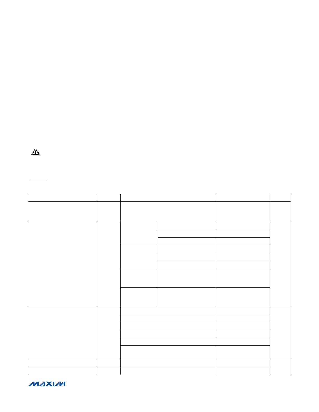
ABSOLUTE MAXIMUM RATINGS
PAVDD, LOVDD, VCOVDD, CPVDD, PLLVDD,
XOVDD, DVDD, and AVDD to EP ....................-0.3V to +3.6V
ENABLE, DATAIN, SDI, SDO, CS, SCLK,
GPO1, GPO2, HOP, and SHDN to EP . -0.3V to (VDD + 0.3V)
All Other Pins to EP .................................. -0.3V to (VDD + 0.3V)
Stresses beyond those listed under “Absolute Maximum Ratings” may cause permanent damage to the device. These are stress ratings only, and functional operation of the device at these or any other conditions beyond those indicated in the operational sections of the specifications is not implied. Exposure to absolute
maximum rating conditions for extended periods may affect device reliability.
CAUTION! ESD SENSITIVE DEVICE
DC ELECTRICAL CHARACTERISTICS
(Figure 2, 50I system impedance, VDD = +2.1V to +3.6V, fRF = 868MHz, TA = -40°C to +125°C, unless otherwise noted. Typical
values are at VDD = +3.0V, TA = +25°C, unless otherwise noted. All min and max values are 100% tested at TA = +125°C and are
guaranteed by design and characterization over temperature, unless otherwise noted.)
Continuous Power Dissipation (TA = +70NC)
TQFN (single-layer board)
(derate 21.3mW/NC above +70NC) ......................... 1702.1mW
Operating Temperature Range ........................ -40NC to +125NC
Storage Temperature Range ............................ -65NC to +150NC
Lead Temperature (soldering, 10s) ................................+300NC
Soldering Temperature (reflow) ......................................+260NC
PARAMETER SYMBOL CONDITIONS MIN TYP MAX UNITS
Supply Voltage V
Operating Current I
Shutdown Current
Input Low Voltage V
Input High Voltage V
DD
DD
PAVDD, LOVDD, VCOVDD, CPVDD,
PLLVDD, XOVDD, DVDD, and AVDD
connected to power supply
fRF = 315MHz 11.2
PA off
PA off,
PA predriver at
high current
setting
P
= +15dBm
OUT
P
= +10dBm
OUT
TA = +25NC, Sleep mode
TA = +85NC, Sleep mode
TA = +125NC, Sleep mode
TA = +25NC, Shutdown mode (registers reset)
TA = +85NC, Shutdown mode (registers reset)
TA = +125NC, Shutdown mode
(registers reset)
IL
IH
fRF = 434MHz 10.4
fRF = 863MHz to 945MHz 10.2
fRF = 315MHz 13.2
fRF = 434MHz 12.4
fRF = 863MHz to 945MHz 12.2
868MHz +15dBm
matching network with
harmonic filter
868MHz +10dBm
matching network with
harmonic filter
2.1 3.0 3.6 V
41
21
350
600
1700 4000
50
200
1300 3500
0.2 x V
DD
0.8 x V
DD
mA
nA
V
����������������������������������������������������������������� Maxim Integrated Products 5
Page 6
MAX7049
High-Performance, 288MHz to 945MHz
ASK/FSK ISM Transmitter
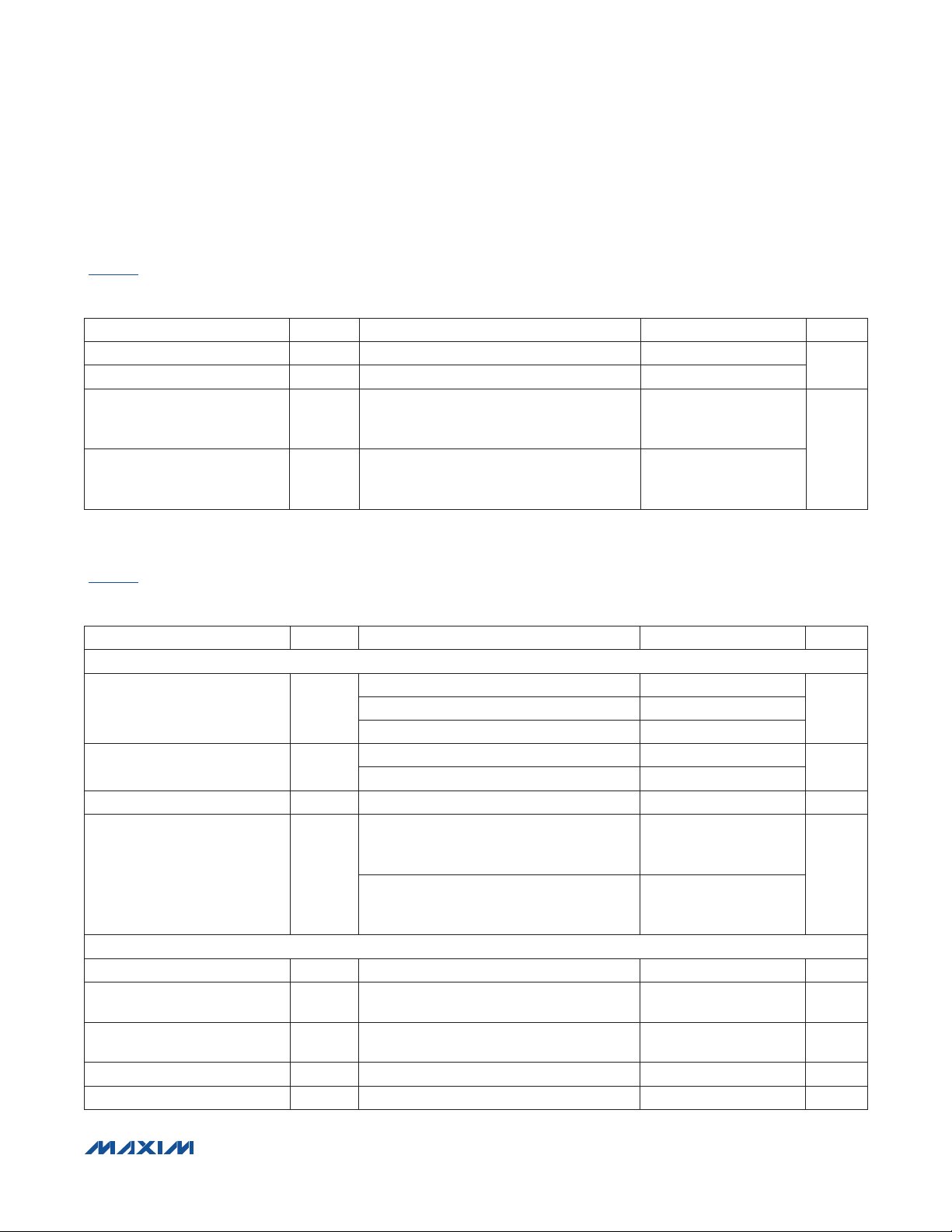
DC ELECTRICAL CHARACTERISTICS (continued)
(Figure 2, 50I system impedance, VDD = +2.1V to +3.6V, fRF = 868MHz, TA = -40°C to +125°C, unless otherwise noted. Typical
values are at VDD = +3.0V, TA = +25°C, unless otherwise noted. All min and max values are 100% tested at TA = +125°C and are
guaranteed by design and characterization over temperature, unless otherwise noted.)
PARAMETER SYMBOL CONDITIONS MIN TYP MAX UNITS
Pulldown Sink Current 12.5
Pullup Source Current 12.5
In buffer mode, GPO1 250FA sink current,
Output Low Voltage V
Output High Voltage V
SDO 1mA sink current, and GPO2 4mA
OL
sink current
In buffer mode, GPO1 250FA source current,
SDO 1mA source current, and GPO2 4mA
OH
source current
0.225
VDD - 0.225
AC ELECTRICAL CHARACTERISTICS
(Figure 2, 50I system impedance, VDD = +2.1V to +3.6V, fRF = 868MHz, TA = -40°C to +125°C, unless otherwise noted. Typical
values are at VDD = +3.0V, TA = +25°C, unless otherwise noted. All min and max values are 100% tested at TA = +125°C and are
guaranteed by design and characterization over temperature, unless otherwise noted.)
FA
V
PARAMETER SYMBOL CONDITIONS MIN TYP MAX UNITS
GENERAL CHARACTERISTICS
Divide-by-1 LO divider setting 863 945
Operating Frequency
Divide-by-3 LO divider setting 287.7 315
Maximum Data Rate
Maximum Frequency Deviation 100kHz synthesizer loop bandwidth
Frequency Settling Time t
POWER AMPLIFIER
Maximum Output Power P
Programmable PA Bias Current
Step
Programmable PA Power
Dynamic Range
Modulation Depth With respect to +10dBm output power 57 dB
Maximum Carrier Harmonics With output matching network -50 dBc
MAX
Manchester encoded 100
NRZ encoded 200
From Enable low-to-high transition to LO
within 5kHz of final value, 100kHz synthesizer
loop bandwidth
ON
From Enable low-to-high transition to LO
within 1kHz of final value, 100kHz synthesizer
loop bandwidth
Match to 50I, including harmonic filter
With Q1% 56.2kI external PA reference
current setting resistor
Power range from decimal 1 to decimal 63
on digital PA bias current
Q150
330
400
+15 dBm
0.5 mA
36 dB
MHzDivide-by-2 LO divider setting 431.5 472.5
kbps
kHz
Fs
����������������������������������������������������������������� Maxim Integrated Products 6
Page 7
MAX7049
High-Performance, 288MHz to 945MHz
ASK/FSK ISM Transmitter
AC ELECTRICAL CHARACTERISTICS (continued)
(Figure 2, 50I system impedance, VDD = +2.1V to +3.6V, fRF = 868MHz, TA = -40°C to +125°C, unless otherwise noted. Typical
values are at VDD = +3.0V, TA = +25°C, unless otherwise noted. All min and max values are 100% tested at TA = +125°C and are
guaranteed by design and characterization over temperature, unless otherwise noted.)
PARAMETER SYMBOL CONDITIONS MIN TYP MAX UNITS
FRACTIONAL-N SYNTHESIZER
VCO Gain K
Close-In Phase Noise 10kHz offset, 100kHz loop BW -101 dBc/Hz
VCO Phase Noise 1MHz offset, 863MHz to 945MHz -126 dBc/Hz
Charge-Pump Current I
LO Divider Settings
Minimum Synthesizer Frequency
Step
Reference Spur -71 dBc
Frequency Switching Time
Reference Frequency Input
Level
ADC
Resolution 7 Bits
LSB Bit Width 7.25 mV
CRYSTAL OSCILLATOR
Crystal Frequency f
Frequency Pulling by V
Recommended Crystal Load
Capacitance
Maximum Crystal Load
Capacitance
TEMPERATURE SENSOR
Range -40 to +125
Digital Code Slope 2
SPI TIMING CHARACTERISTICS (Figure 1)
Minimum SCLK Low to Falling
Edge of CS Setup Time
Minimum CS Low to Rising Edge
of SCLK Setup Time
DD
VCO
XTAL
t
t
CSS
Referenced to 863MHz to 945MHz LO 108 MHz/V
V
= V
CP
SC
OUT
V
= V
OUT
Referenced to 863MHz to 945MHz LO or
carrier frequency band
26MHz frequency step, 902MHz to 928MHz
band, 100kHz synthesizer loop bandwidth
/2, low setting (icont bit = 0) 204
CPVDD
/2, high setting (icont bit = 1) 407
CPVDD
1
2
3
16
f
/2
XTAL
48
1 V
16 to 22.4 MHz
0.5 ppm/V
10
20
20 ns
30 ns
FA
FA
Hz
Fs
P-P
pF
NC
NC/LSB
����������������������������������������������������������������� Maxim Integrated Products 7
Page 8
MAX7049
High-Performance, 288MHz to 945MHz
ASK/FSK ISM Transmitter
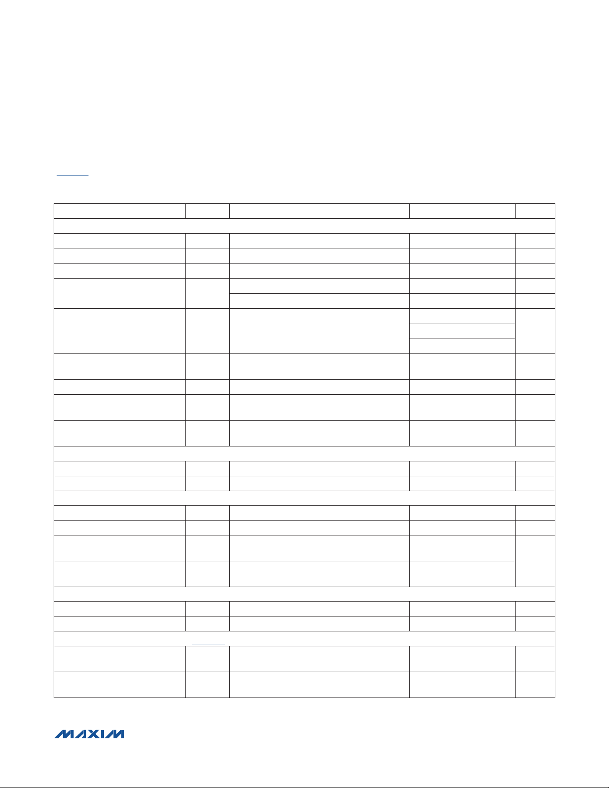
AC ELECTRICAL CHARACTERISTICS (continued)
(Figure 2, 50I system impedance, VDD = +2.1V to +3.6V, fRF = 868MHz, TA = -40°C to +125°C, unless otherwise noted. Typical
values are at VDD = +3.0V, TA = +25°C, unless otherwise noted. All min and max values are 100% tested at TA = +125°C and are
guaranteed by design and characterization over temperature, unless otherwise noted.)
PARAMETER SYMBOL CONDITIONS MIN TYP MAX UNITS
Minimum SCLK Low to Rising
Edge of CS Setup Time
Minimum SCLK Low after Rising
Edge of CS Hold Time
Minimum Data Valid to SCLK
Rising-Edge Setup Time
Minimum Data Valid to SCLK
Rising-Edge Hold Time
Minimum SCLK High Pulse
Width
Minimum SCLK Low Pulse Width t
Minimum CS High Pulse Width
Maximum Transition Time from
Falling Edge of CS to Valid SDO
Maximum Transition Time from
Falling Edge of SCLK to
Valid SDO
t
HCS
t
HS
t
DS
t
DH
t
CH
CL
t
CSH
t
CSG
t
CG
CL = 10pF load capacitance from
SDO to GND
CL = 10pF load capacitance from
SDO to GND
30 ns
20 ns
15 ns
10 ns
30 ns
30 ns
30 ns
20 ns
20 ns
CS
SCLK
SDI
SDO
Figure 1. SPI Timing Diagram
����������������������������������������������������������������� Maxim Integrated Products 8
t
CSH
t
CSS
t
SC
t
DH
t
DS
t
CSG
t
CG
t
HCS
t
CH
t
CL
t
HS
Page 9
MAX7049
High-Performance, 288MHz to 945MHz
ASK/FSK ISM Transmitter
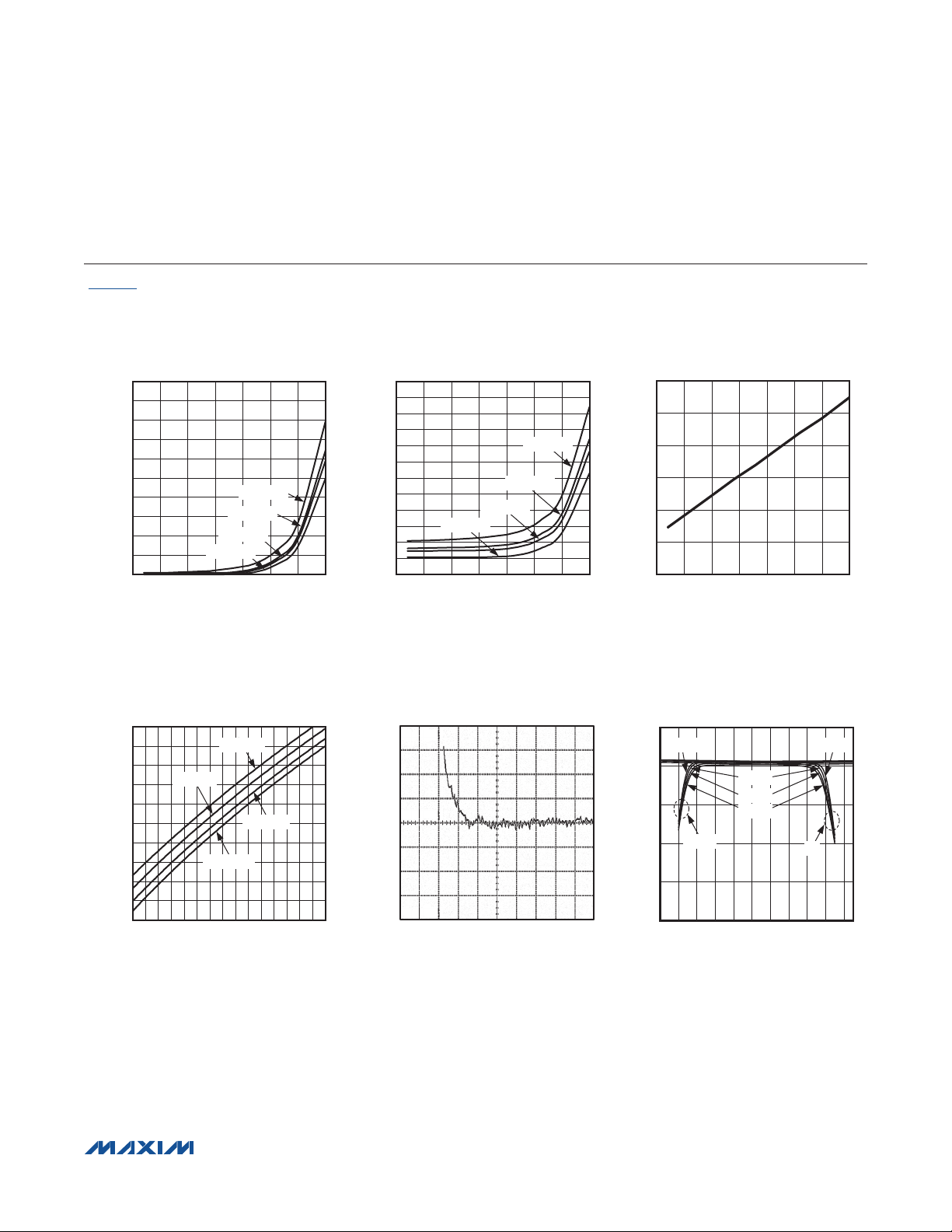
Typical Operating Characteristics
(Figure 2, 50Ω system impedance, VDD = +2.1V to +3.6V, fRF = 288MHz to 945MHz, TA = -40°C to +125°C, unless otherwise noted.
Typical values are at VDD = +3.0V, TA = +25°C, unless otherwise noted.)
SHUTDOWN MODE CURRENT
vs. TEMPERATURE
2.0
1.8
1.6
1.4
1.2
1.0
0.8
0.6
0.4
SHUTDOWN MODE CURRENT (µA)
0.2
0
-50 125
TEMPERATURE (°C)
VDD = 3.6V
VDD = 3.0V
VDD = 2.7V
VDD = 2.1V
VCO TUNING CHARACTERISTIC
(IN 900MHz BAND) vs. CONTROL VOLTAGE
1000
TA = +125˚C
0.7
0.8
TA = -40˚C
0.9
1.0
TA = +85˚C
1.1
1.2
1.3
980
960
940
920
900
880
860
TRANSMIT FREQUENCY (MHz)
840
820
800
TA = +25˚C
0.3
0.4
0.5
CONTROL VOLTAGE WITH RESPECT TO SUPPLY (V)
0.6
SLEEP MODE CURRENT
vs. TEMPERATURE
2.4
2.2
2.0
MAX7049 toc01
1.8
1.6
1.4
1.2
1.0
0.8
0.6
SLEEP MODE CURRENT (µA)
0.4
0.2
0
1007550250-25
-50 125
VDD = 2.1V
TEMPERATURE (°C)
VDD = 3.6V
VDD = 3.0V
VDD = 2.7V
1007550250-25
120
100
MAX7049 toc02
TEMPERATURE SENSOR CODE (DECIMAL)
TEMPERATURE SENSOR CODE
vs. TEMPERATURE
80
60
40
20
0
-50 125
TEMPERATURE (°C)
1007550250-25
MAX7049 toc03
CHARGE-PUMP CURRENT
FREQUENCY SETTLING
AFTER POWER-UP
868.62MHz
MAX7049 toc04
868.60MHz
868.58MHz
1.4
1.5
1.6
1.7
1.8
0.00s
500.0µs 1.000ms
100.0µs/div
MAX7049 toc05
250
200
150
100
CHARGE-PUMP CURRENT (µA)
50
0
vs. CONTROL VOLTAGE
(LOW CURRENT SETTING, 2.1V SUPPLY)
-40˚C-40˚C
+25˚C
+85˚C
+125˚C
DOWN
0 0.2 0.4 0.6 0.8 1.0 1.2 1.4 1.6 1.8 2.0
CONTROL VOLTAGE WITH RESPECT TO GROUND (V)
UP
MAX7049 toc06
����������������������������������������������������������������� Maxim Integrated Products 9
Page 10
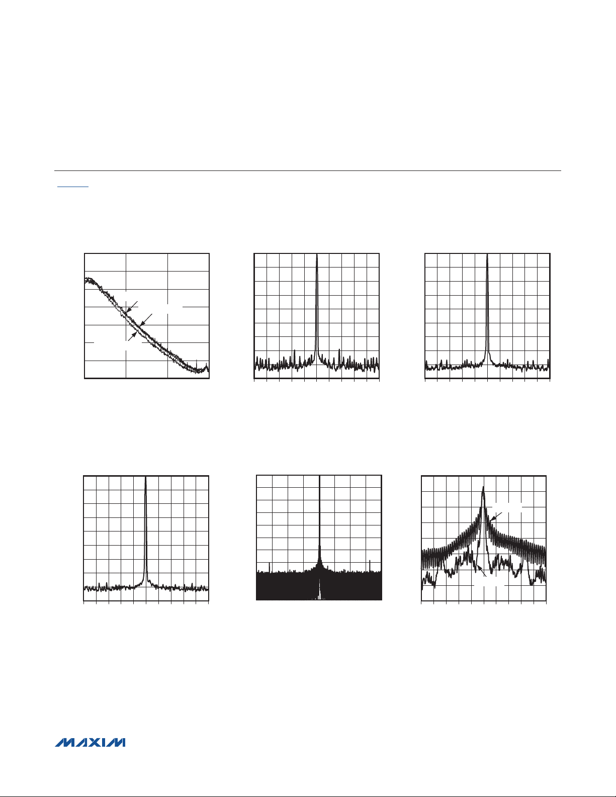
MAX7049
(3kHz RBW, 4kHz SQUARE-WAVE MODULATION,
High-Performance, 288MHz to 945MHz
ASK/FSK ISM Transmitter
Typical Operating Characteristics (continued)
(Figure 2, 50Ω system impedance, VDD = +2.1V to +3.6V, fRF = 288MHz to 945MHz, TA = -40°C to +125°C, unless otherwise noted.
Typical values are at VDD = +3.0V, TA = +25°C, unless otherwise noted.)
PHASE NOISE (VCO DOMINATED)
vs. OFFSET FREQUENCY
(C
= 0.1µF, CS = 0.01µF,
L
R = 200I, RP = CP = 0)
-70
-80
-90
-100
-110
PHASE NOISE (dBc/Hz)
-120
-130
-140
10 10,000
868MHz, ibsel = 0
927MHz, ibsel = 0
927MHz, ibsel = 1
OFFSET FREQUENCY (kHz)
UNMODULATED CLOSE-IN SPECTRUM
(100Hz RBW, 100 SAMPLE AVERAGE,
16MHz CRYSTAL, ibsel = 0, icont = 0)
0
-10
-20
-30
-40
-50
POWER (dBc)
-60
-70
-80
-90
926.990
926.994 926.998 927.002 927.006 927.010
926.992 926.996 927.000 927.004 927.008
FREQUENCY (MHz)
UNMODULATED CLOSE-IN SPECTRUM
(100Hz RBW, 100 SAMPLE AVERAGE,
22.4MHz CRYSTAL, ibsel = 0, icont = 0)
0
-10
MAX7049 toc07
-20
-30
-40
-50
POWER (dBc)
-60
-70
-80
1000100
-90
868.590
868.594 868.598 868.602 868.606 868.610
868.592 868.596 868.600 868.604 868.608
FREQUENCY (MHz)
MAX7049 toc08
UNMODULATED SPECTRUM
UNMODULATED CLOSE-IN SPECTRUM
(100Hz RBW, 100 SAMPLE AVERAGE,
22.4MHz CRYSTAL, ibsel = 0, icont = 0)
0
-10
-20
-30
-40
-50
POWER (dBc)
-60
-70
-80
-90
926.990
926.994 926.998 927.002 927.006 927.010
926.992 926.996 927.000 927.004 927.008
FREQUENCY (MHz)
ASK MODULATION SPECTRUM
MAX7049 toc09
(palopwr = 0, 100% DUTY CYCLE,
MAX7049 toc10
+10dBm, 868MHz,
WITH +10dBm AT 3V MATCH)
0
-10
-20
-30
-40
-50
POWER (dBc)
-60
-70
-80
-90
-100
848 888
FREQUENCY (MHz)
MAX7049 toc11
883878868 873858 863853
+10dBm OUTPUT POWER, WITH
+10dBm AT 3V MATCH)
0
-10
-20
-30
-40
POWER (dBc)
-50
-60
-70
-80
867.75
867.85 867.95 868.05 868.15 868.25
867.80 867.90 868.00 868.10 868.20
GAUSSIAN
FREQUENCY (MHz)
UNSHAPED
MAX7049 toc12
���������������������������������������������������������������� Maxim Integrated Products 10
Page 11
MAX7049
POWER (dBc)
(1kHz RBW, 4kHz SQUARE-WAVEMODULATION,
High-Performance, 288MHz to 945MHz
ASK/FSK ISM Transmitter
Typical Operating Characteristics (continued)
(Figure 2, 50Ω system impedance, VDD = +2.1V to +3.6V, fRF = 288MHz to 945MHz, TA = -40°C to +125°C, unless otherwise noted.
Typical values are at VDD = +3.0V, TA = +25°C, unless otherwise noted.)
ASK MODULATION SPECTRUM
(3kHz RBW, 4kHz SQUARE-WAVE MODULATION,
+9dBm OUTPUT POWER, WITH
+10dBm AT 3V MATCH)
0
-10
-20
-30
-40
-50
-60
-70
-80
867.75
867.85 867.95 868.05 868.15 868.25
867.80 867.90 868.00 868.10 868.20
GAUSSIAN
FREQUENCY (MHz)
FSK MODULATION SPECTRUM
(3kHz RBW, 4kHz SQUARE-WAVE MODULATION,
Q100kHz DEVIATION, +10dBm OUTPUT
POWER, WITH +10dBm AT 3V MATCH)
0
-10
GAUSSIAN
-20
-30
-40
-50
POWER (dBc)
-60
-70
-80
-90
867.4 867.8 868.2 868.6867.6 868.0 868.4
UNSHAPED
FREQUENCY (MHz)
MAX7049 toc13
FSK MODULATION SPECTRUM (1kHz RBW,
4kHz SQUARE-WAVE MODULATION,
±4kHz DEVIATION, +10dBm OUTPUT
POWER, WITH +10dBm AT 3V MATCH)
0
-10
GAUSSIAN
-20
-30
-40
POWER (dBc)
-50
-60
-70
-80
867.95 867.97 867.99 868.01 868.03 868.05
867.96 867.98 868.00 868.02 868.04
MAX7049 toc16
FREQUENCY (MHz)
FSK MODULATION SPECTRUM
±4kHz DEVIATION, +10dBm OUTPUT POWER,
WITH +10dBm AT 3V MATCH)
0
-10
MAX7049 toc14
UNSHAPED
-20
-30
-40
POWER (dBc)
-50
-60
-70
-80
867.95 867.97 867.99 868.01 868.03 868.05
FREQUENCY (MHz)
FSK MODULATION SPECTRUM
(3kHz RBW, 4kHz SQUARE-WAVE MODULATION,
Q100kHz DEVIATION, +10dBm OUTPUT
POWER, WITH +10dBm AT 3V MATCH)
0
-10
UNSHAPED
-20
-30
-40
-50
POWER (dBc)
-60
-70
-80
-90
867.4 867.8 868.2 868.6867.6 868.0 868.4
FREQUENCY (MHz)
MAX7049 toc15
MAX7049 toc17
���������������������������������������������������������������� Maxim Integrated Products 11
Page 12
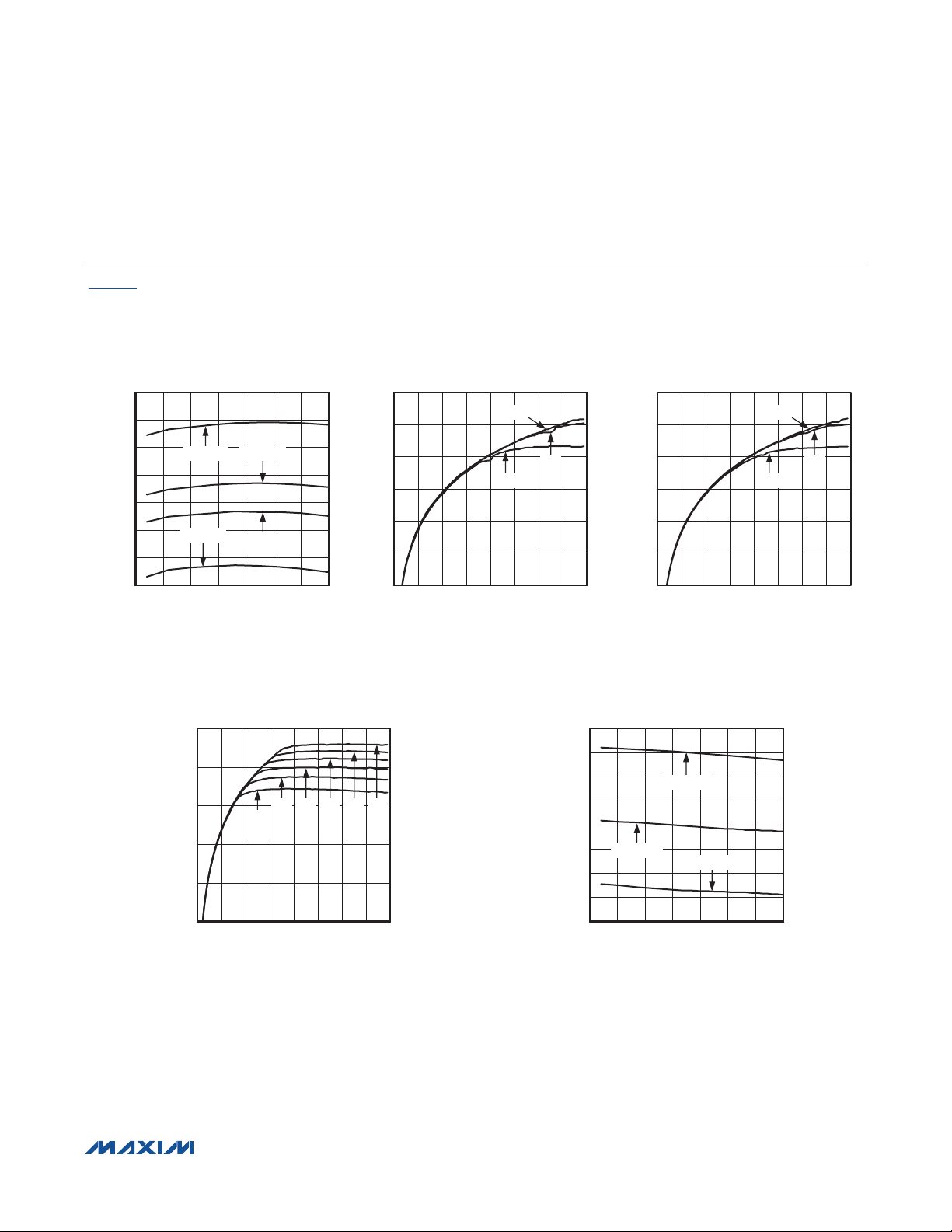
MAX7049
High-Performance, 288MHz to 945MHz
ASK/FSK ISM Transmitter
Typical Operating Characteristics (continued)
(Figure 2, 50Ω system impedance, VDD = +2.1V to +3.6V, fRF = 288MHz to 945MHz, TA = -40°C to +125°C, unless otherwise noted.
Typical values are at VDD = +3.0V, TA = +25°C, unless otherwise noted.)
Tx CURRENT vs. TEMPERATURE
(PA OFF, 900MHz BAND, palopwr = 1)
10.60
10.50
10.40
10.30
10.20
Tx CURRENT (mA)
10.10
10.00
9.90
-50 125
VDD = 3.6V
VDD = 2.1V
TEMPERATURE (°C)
VDD = 3.0V
VDD = 2.7V
PA POWER vs. PA CODE
(palopwr = 1, 100% DUTY CYCLE, 868MHz,
WITH +10dBm AT 3V MATCH)
15
10
5
(dBm)
OUT
P
0
-5
-10
0 64
2.1V
PA CODE (DECIMAL)
20
15
MAX7049 toc18
10
(dBm)
OUT
P
1007550250-25
2.4V 2.7V 3.0V 3.3V 3.6V
-10
5648403224168
(palopwr = 0, 100% DUTY CYCLE, 915MHz,
PA POWER vs. PA CODE
WITH +15dBm AT 3V MATCH)
3.6V
3.0V
5
0
-5
0 64
PA CODE (DECIMAL)
2.1V
5648403224168
(palopwr = 0, 100% DUTY CYCLE, 868MHz,
14
(dBm)
OUT
P
12
10
8
6
4
2
0
-2
MAX7049 toc21
(palopwr = 0, 100% DUTY CYCLE, 868MHz,
PA POWER vs. PA CODE
WITH +15dBm AT 3V MATCH)
20
3.6V
2.1V
MAX7049 toc19
15
10
(dBm)
5
OUT
P
0
-5
-10
0 64
PA CODE (DECIMAL)
PA POWER vs. PA CODE
WITH +15dBm AT 3V MATCH)
PA CODE 39
PA CODE 19
-50 125
PA CODE 10
10075-25 0 25 50
TEMPERATURE (°C)
MAX7049 toc20
3.0V
5648403224168
MAX7049 toc22
���������������������������������������������������������������� Maxim Integrated Products 12
Page 13
MAX7049
High-Performance, 288MHz to 945MHz
ASK/FSK ISM Transmitter
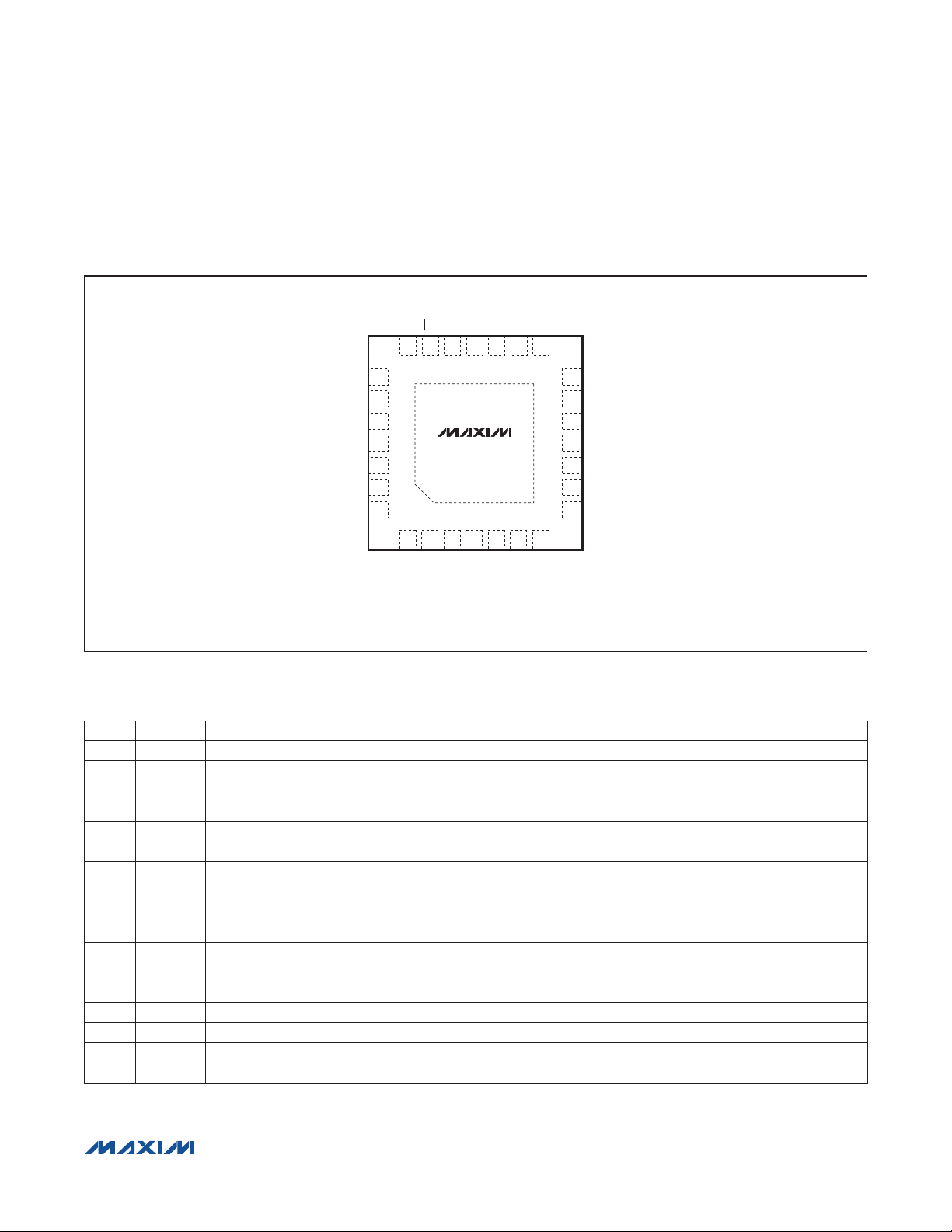
Pin Configuration
TOP VIEW
CS
SCLK
SDI
18
4 5 6 7
N.C.
LOVDD
ENABLE
EP
CTRL
VCOVDD
DATAIN
SDO
CPVDD
14
N.C.
XTALB
13
12
XTALC
XOVDD
11
10
N.C.
PLLVDD
9
8
CPOUT
DVDD
HOP
GPO1
SHDN
AVDD
PA+
PA-
GPO2
2021 19 17 16 15
22
23
24
25
26
27
28
1 2
+
PAVDD
MAX7049
3
REXTPA
TQFN
(5mm x 5mm)
Pin Description
PIN NAME FUNCTION
1 PAVDD Power Amplifier Supply Voltage Input. Bypass to ground with 33pF capacitor as close as possible to the pin.
External PA Bias Current Setting Resistor Connection. Couple to ground through a Q1% tolerance low-
2 REXTPA
3, 10,
14
N.C. No Connection. Leave unconnected.
4 LOVDD
5 VCOVDD
6 CTRL
7 CPVDD
8 CPOUT Charge-Pump Output. Connect through passive loop filter to CTRL.
9 PLLVDD Synthesizer Supply Voltage Input. Bypass to ground with 33pF capacitor as close as possible to the pin.
11 XOVDD
temperature coefficient resistor. A resistor of 56.2kI is recommended for a 0.5mA nominal PA bias
current DAC LSB value.
Local Oscillator (LO) Supply Voltage Input. Bypass to ground with 33pF capacitor as close as possible
to the pin.
Voltage-Controlled Oscillator (VCO) Supply Voltage. Bypass to ground with 1FF capacitor as close as
possible to the pin.
Control (Tuning) Voltage for VCO Input. Referenced to VCOVDD pin. Connect through passive loop filter to
CPOUT.
Charge-Pump Supply Voltage Input. Bypass to ground with 0.01FF capacitor as close as possible to the pin.
Crystal Oscillator Supply Voltage Input. Bypass to ground with 0.1FF capacitor as close as possible to
the pin.
���������������������������������������������������������������� Maxim Integrated Products 13
Page 14

MAX7049
High-Performance, 288MHz to 945MHz
ASK/FSK ISM Transmitter
Pin Description (continued)
PIN NAME FUNCTION
Collector Crystal Input. Connect to crystal either directly or through an AC-coupling capacitor. A shunt
12 XTALC
13 XTALB
15 SDO Serial Peripheral Interface (SPI) Data Output. It can also be configured as a general-purpose digital output.
16 DATAIN Transmitter Data Input. The Datain function can also be controlled by SPI. Internally pulled to ground.
17 ENABLE
18 SCLK SPI Clock. Internally pulled to ground.
19 SDI SPI Data Input. Internally pulled to ground.
20
21 GPO2 General-Purpose Output 2. High drive strength digital general-purpose output.
22 DVDD
23 HOP
24 GPO1 General-Purpose Output 1. Low drive strength digital general-purpose output.
25 SHDN
26 AVDD
27 PA+
28 PA-
— EP
CS
capacitance to ground might be needed depending on the specified load capacitance of the crystal and
PCB stray capacitances. Can be driven by an AC-coupled external reference with a signal swing of
0.8V
Base Crystal Input. Connect to crystal either directly or through an AC-coupling capacitor. A shunt
capacitance to ground might be needed depending on the specified load capacitance of the crystal and
PCB stray capacitances. Must be DC shorted to ground if XTALC is driven by external reference.
Enable. Drive high for active operation. Drive low or leave unconnected to put the device into Sleep mode.
The enable function can also be controlled by SPI. Internally pulled to ground.
SPI Active-Low Chip Select. Internally pulled to supply.
Digital Supply Voltage Input. Bypass to ground with 0.1FF capacitor as close as possible to the pin.
Frequency Hop Pin. Transfers the base[20:0] bits to the fractional-N divider. See the Fractional-N Synthesizer
section. The hop function can also be controlled by SPI. Internally pulled to ground.
Shutdown Digital Input. Turns off internal power-on-reset (POR) circuit when driven high. Register contents
are set to the initial state when driven high. Must be driven low for normal operation. Not internally pulled to
supply or ground.
Analog Supply Voltage Input. Bypass to ground with a 1FF capacitor as close as possible to the pin.
Power Amplifier (PA) Positive Output. Requires DC current path to supply voltage through an inductive path.
The DC current path can be part of the output impedance matching and harmonic filter network.
Power Amplifier (PA) Negative Output. Requires DC current path to supply voltage through an inductive path.
The DC current path can be part of the output impedance matching and harmonic filter network.
Exposed Pad. This is the only ground connection. Solder evenly to the PCB ground plane for proper
operation. Multiple vias from the solder pad to the PCB ground plane are recommended.
P-P
to 1.2V
P-P
.
���������������������������������������������������������������� Maxim Integrated Products 14
Page 15
MAX7049
High-Performance, 288MHz to 945MHz
ASK/FSK ISM Transmitter
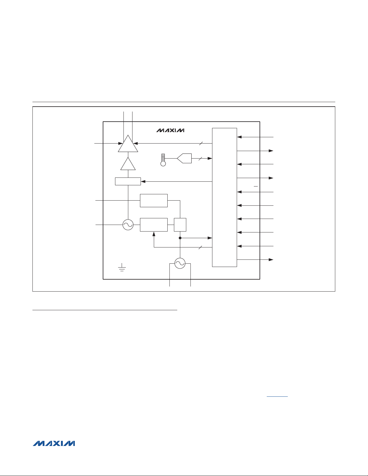
Functional Diagram
27 28
PA-
PA+
25
SHDN*
GPO1*
HOP*
GPO2*
SDI
24
23
21
CS
20
19
2
8
REXTPA
CPOUT
PA
/1, /2, OR /3
TEMPERATURE
SENSOR
CHARGE
PUMP
MAX7049
ADC
6
7
DIGITAL
CONTROL
AND MCU
INTERFACE
6
CTRL
GROUNDED
PAD (EP)
FRACTIONAL-N
DIVIDER
VCO
XTAL OSCILLATOR
XTALC
12 13
Detailed Description
Architectural Overview and
Applications Circuit
The MAX7049 includes a single precision local oscillator
fractional-N synthesizer with an integrated VCO, fractional-N divider, phase/frequency detector, charge pump,
LO divider, and lock detector. The loop filter is located
off-chip to allow the user to optimize the synthesizer noise
and transient characteristics for a particular application.
In FSK transmit mode, the synthesizer transitions between
the mark and the space frequency based on the state
of the DATAIN pin or datain bit (Datain register, 0x3D,
bit 6). A user-programmable frequency-shaping function
enables the user to precisely define the transition from the
mark frequency to the space frequency and vice versa to
minimize spectral width of the modulated Tx waveform.
The IC utilizes a differential emitter-coupled, dual-opencollector power amplifier for the transmitter output.
SCLK 18
PFD
XTALB
21
* OPTIONAL I/Os FROM/ TO MCU.
DATAIN*
SDO*
17ENABLE*
16
15
The bias current of the output stage is set with a combination of an external resistor and an internal amplitudeshaping function. The programmable shaping function enables the user to precisely define the transition
between carrier on and carrier off and vice versa based
on the state of the DATAIN pin or datain bit so as to
minimize the spectral width of the modulated Tx signal.
Linear amplitude ramping is used in FSK mode as the PA
is enabled at the beginning of a data burst and disabled
at the end of a data burst for spectral control.
A complete transmitter system can be built using a
low-end MCU, the IC, a crystal, and a small number of
passive components for power-supply bypassing and for
RF matching, as illustrated in Figure 2.
Communication between the MCU and the IC is accomplished through a 4-pin SPI bus and a number of optional
digital inputs and outputs.
���������������������������������������������������������������� Maxim Integrated Products 15
Page 16

MAX7049
High-Performance, 288MHz to 945MHz
ASK/FSK ISM Transmitter
C13
L1
50I
C20
PAVDD
N.C.
LOVDD
CTRL
CPVDD
1
2
3
4
5
6
7
C14
L2
PA-
+
2728 26 25 24 23 22
J1
C17
R2
L4
C16 C15
V
DD
C1
R1
C2
C3
C4
L3
REXTPA
VCOVDD
PA+
C12
AVDD
MAX7049
GROUNDED
PAD (EP)
DASHED LINES DENOTE OPTIONAL CONNECTIONS
SHDN
GPO1
HOP
DVDD
C11
GPO2
21
CS
20
SDI
19
SCLK
18
ENABLE
17
DATAIN
16
SDO
15
µP
C6
C5
Figure 2. Typical Operating Circuit
���������������������������������������������������������������� Maxim Integrated Products 16
CPOUT
98 10
PLLVDD
C7
N.C.
12
11
XOVDD
C8
13 14
XTALB
XTALC
Y1
C9 C10
N.C.
Page 17

MAX7049
High-Performance, 288MHz to 945MHz
ASK/FSK ISM Transmitter
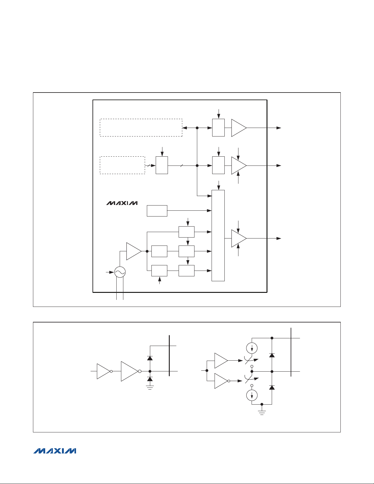
Digital Inputs and Outputs
Digital Inputs
The IC’s SPI inputs are the CS, SCLK, and SDI pins. The
CS pin is active low, so this pin has an internal pullup.
The SCLK and SDI pins have internal pulldowns. In addition to the SPI inputs, there are also a number of optional
digital inputs to the IC. These inputs are DATAIN,
ENABLE, and HOP. These optional inputs, which have
internal pulldowns, give the user the option to control an
internal signal by either driving the pin to the appropriate
logic level or by setting a control bit to the appropriate
state. This is illustrated in Figure 3.
SPI control minimizes the number of I/Os required
between the IC and the MCU, whereas the pin control
eliminates the configuration overhead associated with
SPI communication.
DVDD
22
20
CS
INTERNAL
CSB
SIGNAL
DVDD
22
INPUT INPUT
Digital Outputs
The IC has two dedicated general-purpose outputs
(GPO1 and GPO2), one SPI output (SDO) that can also
serve as a general-purpose output when CS is high. The
GPO1, GPO2, and SDO pins can be configured to output
various internal status signals and clocks, as illustrated
in Figure 4.
The outputs (GPO1 and GPO2) offer a feature where the
pin can operate either as a digital buffer or as a currentlimited source/sink output, as illustrated in Figure 5.
22
DVDD
INTERNAL
INPUT
SIGNAL
‘OR’
INTERNAL
INPUT
SIGNAL
GROUNDED
PAD (EP)
Figure 3. Digital Inputs
SPI INPUTS
GROUNDED
PAD (EP)
GROUNDED
PAD (EP)
INPUT = DATAIN, ENABLE, AND HOPINPUT = SCLK AND SDI
INPUT PROGRAMMABLE
Table 1. Optional Digital Input Controls
PIN BIT NAME
DATAIN datain Datain 0x3D 6 Data input to transmitter.
ENABLE enable EnableReg 0x3E 0 Enable input for transmitter.
HOP hop FLoad 0x0B 0
���������������������������������������������������������������� Maxim Integrated Products 17
REGISTER
NAME
REGISTER
ADDRESS (hex)
BIT LOCATION
(7:0)
FUNCTION
Initiates the transition to the next
frequency as defined by base[20:0].
CONTROL BIT
Page 18
MAX7049
High-Performance, 288MHz to 945MHz
ASK/FSK ISM Transmitter
sdos[3:0]
SPI READ-ONLY REGISTERS
TestBus0 AND TestBus1 (0x40 AND 0x41)
INTERNAL SIGNALS
MAX7049
clksht
XTALC13XTALB
12
tmux[3:0]
MUX
plllock
xtal
/16
/5, /6,
/7, OR /8
xtal
[1:0]
tbus[15:0]
mclk
ckdiv[1:0]
/1, /2,
/4, OR /8
/1, /2,
/4, OR /8
/1, /2,
/4, OR /8
[15:4]
MUX
gp1s[3:0]
MUX
gp2s[3:0]
MUX
gp1md[1:0]
gp1isht
gp2md[2:0]
gp2isht
SDO 15
GPO1 24
GPO2
21
Figure 4. Digital Outputs
INTERNAL
SIGNAL
Figure 5. Digital Output Options
���������������������������������������������������������������� Maxim Integrated Products 18
BUFFER MODE CURRENT MODE
DVDD
OUTPUT
GROUNDED
PAD (EP)
22
INTERNAL
SIGNAL
I
SOURCE
I
SINK
GROUNDED
PAD (EP)
DVDD
OUTPUT
22
Page 19

MAX7049
High-Performance, 288MHz to 945MHz
ASK/FSK ISM Transmitter
The current mode of operation can reduce digital noise
associated with large supply current spikes. The GPO1
pin has a relatively small current drive capability (80µA
or 160µA). The IOConf2 register (0x05) (gp1md[1:0] bits)
control the current settings:
gp1md[1:0] Mode
0x Buffer mode
10 80µA sink/source capability
11 160µA sink/source capability
GPO2 has a much larger current drive capability (up to
4mA), as this GPO can be the source of output clock
signals. The IOConf2 register (0x05) (gp2md[2:0] bits)
control the current settings:
gp2md[2:0] Mode
0xx Buffer mode
100 1.0mA sink/source capability
101 2.0mA sink/source capability
110 3.0mA sink/source capability
111 4.0mA sink/source capability
Two other bits also control the operation of GPO1 and
GPO2. The IOConf0 register (0x03) (gp1isht and gp2isht
bits) allows the current mode operation to continue even
if the IC is disabled (Sleep mode).
The GPO2 pin is designated as the primary output for
driving a clock, as it has the strongest buffer and highest
current output capabilities.
The GPO2 clock signal can be selected by the gp2s[3:0]
and ckdiv[1:0] bits (IOConf0 register, 0x03).
gp2s[3:0] GPO2 Output
0000 plllock
0001 mclk /(ckdiv divider)
0010 xtal/(ckdiv divider)
0011 xtal/16/(ckdiv divider)
where the ckdiv divider is given by:
ckdiv[1:0] Divide by
00 1
01 2
10 4
11 8
and xtal is the crystal frequency, and mclk is the master
digital clock. The master digital clock is the divided crystal
frequency given by the xtal[1:0] bits (Conf0 register, 0x01),
according to:
xtal[1:0] Divide by
00 5
01 6
10 7
11 8
If a clock output on GPO2 is required even when the IC
is in Sleep mode (ENABLE pin and enable bit reset to 0),
the SHDN pin is reset to 0, and the clksht bit (IOConf2
register, 0x05, bit 3) must be set to 1.
A very useful function of the GPOs is to output status
signals that reflect the state of the transmitter at any
particular instance in time. See the Register Details
section for an in-depth description of the status signals
available for the TestBus0 and TestBus1 registers.
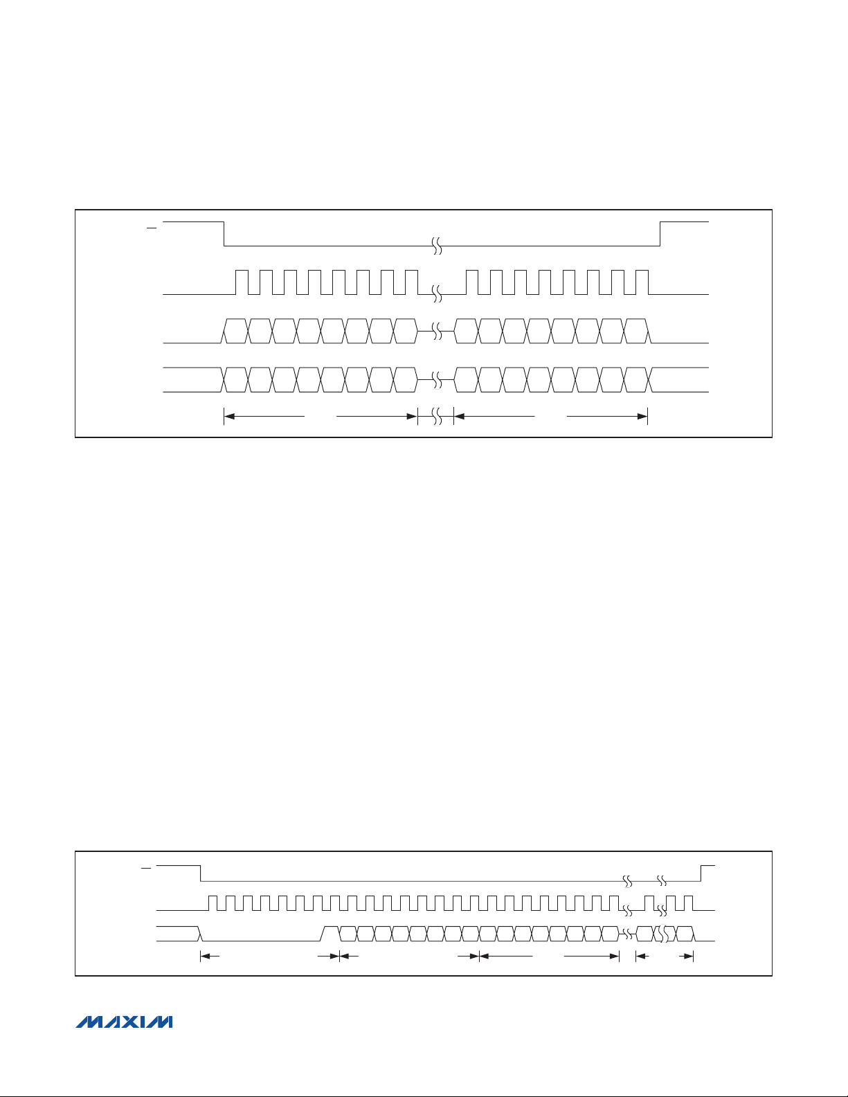
Serial Peripheral Interface (SPI)
The IC utilizes a 4-wire SPI protocol for programming its
registers, configuring and controlling the operation of the
whole transmitter.
The following digital pins control the operation of the SPI:
CS: Active-low SPI chip select
SDI: SPI data input
SCLK: SPI serial clock
SDO: SPI data output
The SPI operates on a byte format, as shown in Figure 6.
Any number of 8-bit data bursts (Data 1, Data 2, … Data
N) can be sent within one low cycle of CS, to allow for
burst-write or burst-read operations. The SDO pin acts
as another general-purpose output (GPO) when the CS
pin is high.
���������������������������������������������������������������� Maxim Integrated Products 19
Page 20
SCLK
MAX7049
High-Performance, 288MHz to 945MHz
ASK/FSK ISM Transmitter
CS
SDI
SDO
Figure 6. SPI Format
DI7 DI6 DI5 DI4 DI3 DI2 DI1 DI0
DO7 DO6 DO5 DO4 DO3 DO2 DO1 DO0
DATA 1
DI7 DI6 DI5 DI4 DI3 DI2 DI1 DI0
DO7 DO6 DO5 DO4 DO3 DO2 DO1 DO0
DATA N
SPI Commands
The following commands are implemented in the IC:
Write: Within the same CS cycle, a write command is implemented as follows:
SDI: <0x01> <Initial Address> <Data 1> <Data 2> … <Data N>
With this command, Data 1 is written to the address given by <Initial Address>, Data 2 is written to <Initial Address +
1>, and so on.
Read: Within the same CS cycle, a read command is implemented as follows:
SDI: <0x02> <Address 1> <Address 2> <Address 3> … <Address N> <0x00>
SDO: <0xXX> <0xXX> <Data 1> <Data 2> … <Data N - 1> <Data N>
With this command, all the registers can be read within the same cycle of CS. The addresses can be given in any order.
Read All: With two CS cycles, the Read All command is implemented as follows:
CS Cycle 1 CS Cycle 2
SDI: <0x03> <Address N> <0x00> <0x00> <0x00> … <0x00>
SDO: <Data N> <Data N + 1> <Data N + 2> … <Data N + n>
Reset: A SPI reset command is implemented as follows:
SDI: <0x04>
An internal active-low master resetb signal is generated, from the falling edge of the last SCLK signal to the falling edge
of the following CS signal (t
HCS
+ t
CSH
).
CS
SCLK
SDI
WRITE COMMAND (0x01)
Figure 7. SPI Write Command Format
���������������������������������������������������������������� Maxim Integrated Products 20
A7 A6 A5 A4 A3 A2 A1 A0 D7 D6 D5D4D3 D2 D1 D0
INITIAL ADDRESS (A[7:0]) DATA 1 DATA N
D7 D0
Page 21
SCLK
MAX7049
High-Performance, 288MHz to 945MHz
ASK/FSK ISM Transmitter
CS
SDI
READ COMMAND (0x02) ADDRESS 1 ADDRESS 2 ADDRESS N 0x00
SDO
Figure 8. SPI Read Command Format
CS
SCLK
SDI
READ-ALL COMMAND (0x03)
SDO
Figure 9. SPI Read-All Command Format
CS
A7 A6 A5 A4 A3A2A1 A0
A7 A6 A5 A4 A3 A2 A1 A0
ADDRESS N
A7 A0A7A6 A5 A4 A3A2A1
D7 D6 D5 D4 D3
DATA 1 DATA 2 DATA N
D7 D6 D5 D4 D3 D2 D1 D0 D7 D0D0D7
A0
D2
D1 D0 D7 D0D0D7
DATA N + 1DATA N
INITIAL
SHUTDOWN
DATA N + n
SCLK
SLEEP
SDI
resetb
SLEEP
XTAL ON
RESET COMMAND (0x04)
CONFIGURATION
Figure 10. SPI Reset Command Format Figure 11. Operating Modes
Operating Mode Overview
The IC offers several modes of operation that allow the
user to optimize the transmitter’s power consumption for
a particular application. The primary operating modes
are Initial, Sleep, Temperature Sensor, and Tx, as illustrated in Figure 11.
When the SHDN pin is high, the IC is in Shutdown mode.
In Shutdown mode, the POR circuit internal to the IC is
disabled and draws virtually no current. In Shutdown
mode, all internal data registers are reset to the initial
states and must be rewritten for desired transmitter
operation after the SHDN pin is driven low.
���������������������������������������������������������������� Maxim Integrated Products 21
SPI
FSK
ASK
TEMPERATURE
SENSOR
Tx
Page 22

MAX7049
High-Performance, 288MHz to 945MHz
ASK/FSK ISM Transmitter
When the SHDN pin is low, the POR circuit is active and
holds the internal data registers in the initial state until the
power supply is above 2.1V and the IC enters the Initial
mode. From the Initial mode, the IC can be configured
for operation in Sleep mode, Temperature Sensor mode,
or Tx mode. In Sleep mode, there are two options available: Sleep and XTAL ON. In Sleep mode, the current
drain is typically 350nA. All register states are retained in
Sleep mode. In XTAL ON mode, controlled by the clksht
bit (IOConf2 register, 0x05, bit 3), the crystal oscillator is
enabled and the divided output of the crystal oscillator
(/1, /2, /4, /8, as set by the ckdiv[1:0] bits (IOConf0 register, 0x03, bits [5:4]) can be directed to GPO2. The XTAL
ON mode is designed so an accurate high-speed clock
is always available to the MCU.
In Temperature Sensor mode, the internal temperature
sensor function can be executed.
In Tx mode, the transmitter can be configured to transmit
ASK data or FSK data.
Table 2. Mode Control Logic
SHDN PIN ENABLE PIN enable BIT
0 0 0 Sleep
0 0 1 Tx
0 1 0 Tx
0 1 1 Tx
1 0 0 Shutdown
1 0 1 Shutdown
1 1 0 Shutdown
1 1 1 Shutdown
TRANSMITTER
MODE
The Tx mode is determined by the logic states of the
SHDN pin, ENABLE pin, and the enable bit (EnableReg
register, 0x3E, bit 0). The transmitter is enabled if the
SHDN pin is driven low and the ENABLE pin is driven
high, or the enable bit is set. This logic is summarized
in Table 2.
The mode options are selected by the mode SPI bit
(Conf0 register, 0x01, bit 4) and these options are
summarized in Table 3.
Sleep Mode
From the Initial mode, the transmitter directly enters
Sleep mode. In XTAL ON mode, the crystal oscillator is
enabled and the divided output of the crystal oscillator
can be directed to GPO2. This mode is enabled when
the RF functions are disabled and the clksht bit is set.
The current drain in this mode is highly dependent on the
frequency of the output signal and the load capacitance
on the GPO2 pin. The current drain is typically 750µA
when the output signal is 3.2MHz and the load capacitance is 10pF. See the Digital Outputs section for more
details. Table 4 summarizes the Sleep mode functions.
Table 4. Sleep Mode Summary
SLEEP
MODE
Sleep Enable = 0 350nA
XTAL
ON
*Dependent on GPO2 load capacitance and output clock
frequency.
SETTINGS
clksht = 1
TYPICAL
CURRENT
DRAIN
750FA*
COMMENTS
All register contents
are retained.
Divided XTAL
oscillator signal can
be directed to GPO2.
Table 3. Mode Option Logic
mode BIT MODE OPTION
0 ASK
1 FSK
���������������������������������������������������������������� Maxim Integrated Products 22
Page 23

MAX7049
High-Performance, 288MHz to 945MHz
ASK/FSK ISM Transmitter
Temperature Sensor Mode
The user must initiate the temperature sensor from Sleep
mode, and the transmitter automatically returns to sleep
when the measurement sequence is completed.
The on-chip temperature sensor is enabled when the
tsensor bit (EnableReg register, 0x3E, bit 3) is set. Once
the internal analog temperature sensor circuit has settled,
an A/D conversion is performed and the resultant ADC
value is stored in the tsadc[6:0] bits that are accessed
through the TestBus1 register (0x41, bits 6:0) when the
digital test mux bits tmux[3:0] (TestMux register, 0x3C,
bits 3:0) are set to 0. The tsensor bit is a self-reset bit,
so it returns to a zero state once the temperature sensor
measurement is completed. The tsdone status bit (Status1
register, 0x43, bit 4) is also set when the measurement
is completed. The current drain in Temperature Sensor
mode is less than 1mA and the sensor settling time plus
the ADC conversion time is less than 2ms. The pertinent
features of the Temperature Sensor mode are summarized in Table 5.
Tx Mode
There are two subsets of the Tx mode. These subsets
include FSK and ASK.
The transmitter output signal is generated by the fractional-N
synthesizer, then buffered, and amplified by the power
amplifier (PA) to the programmed output power level. There
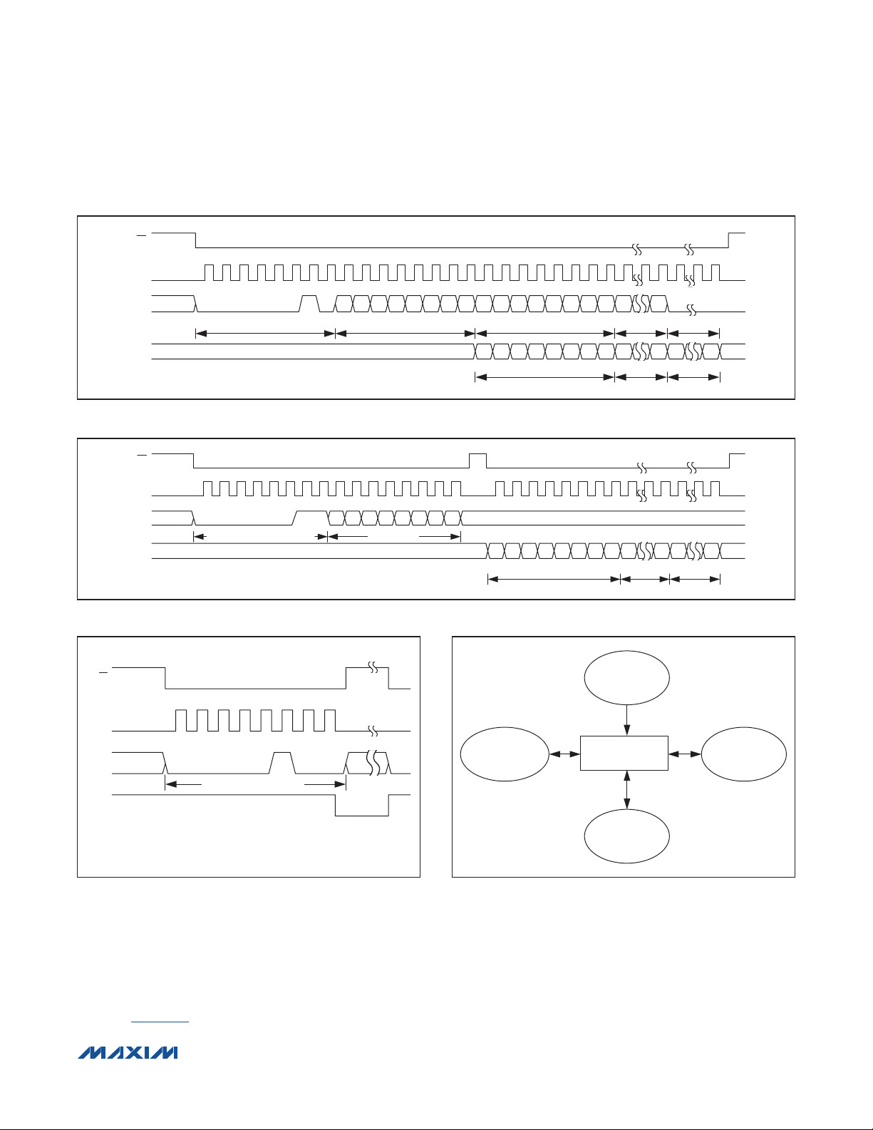
is a finite warmup time for the transmitter. Upon entering Tx
mode from Sleep mode, the following sequence occurs:
1) The crystal oscillator is enabled and settles to a steady
state. The rising edge of the internal ckalive status signal indicates that the crystal oscillator has settled and
an accurate time base is available. All other Tx modules
are enabled except the PA. The synthesizer settles to
the desired LO frequency at the same time the other
Table 5. Temperature Sensor Mode
Summary
TYPICAL
CURRENT
DRAIN (mA)
COMMENTS
BIT
EXECUTION
TIME (ms)
modules settle to their desired operating points.
A rising edge of the lockdet status signal indicates
that the synthesizer has locked. In some narrowband applications, the lockdet signal can effectively
be delayed with the plldl[2:0] bits (Conf1 register,
0x02, bits 5:3) to ensure that the synthesizer has
settled to within the desired accuracy. This delayed
signal is called plllock. The rising edge of the txready
status signal is coincident with the rising edge of the
plllock signal.
2) In ASK mode, the power amplifier ramp-up sequence
begins on the rising edge of either the DATAIN pin
or the datain bit after the internal txready signal
transitions high. In FSK mode, the power amplifier
linear ramp-up sequence begins on the rising edge
of the txready signal.
Figure 12 illustrates this warmup sequence.
In an ASK application, the output of the synthesizer
is fixed at the carrier frequency. The output power is
alternated between fully off when both the DATAIN
pin is logic 0 and the datain bit is cleared, and the
programmed output power level when either the DATAIN
enable
‘OR’
ENABLE
ckalive
lockdet
plllock
txready
datain
‘OR’
DATAIN
PA
Q
105µs
(typ)
95µs
(typ)
plldel
INTERVAL
*
tsensor < 2 < 1
���������������������������������������������������������������� Maxim Integrated Products 23
The tsdone status
bit is set when the
measurement is
completed. The
results are stored in
tsadc[6:0].
USER-DEFINED PA RAMP
(*PA RAMP BEGINS ON THE RISING EDGE OF DATAIN IN ASK MODE
AND ON THE RISING EDGE OF txready IN FSK MODE.)
Figure 12. Tx Warmup Timing Diagram
Page 24

High-Performance, 288MHz to 945MHz
pin is logic 1 or the datain bit is set. The output signal
can be waveshaped in amplitude to reduce the spectral
width of the transmission. See the Power Amplifier section
for more information regarding amplitude waveshaping.
The PA power is determined by the 6-bit amplitude word
that linearly controls the PA output bias current. The LSB
current amplitude is set by an off-chip resistor placed
between the REXTPA pin and ground. The LSB current is
nominally 0.5mA for a 56.2kI resistor and allows for very
tight transmitter power control with a low-temperature
coefficient ±1% tolerance resistor.
In an FSK application, the output of the synthesizer
alternates between the space frequency when both the
DATAIN pin is logic 0 and the datain bit is cleared, and
the mark frequency when either the DATAIN pin is logic 1
or the datain bit is set. The output signal can be waveshaped in frequency to reduce the spectral width of the
transmission. See the Fractional-N Synthesizer section
for more information regarding frequency waveshaping.
The PA power is determined by the 6-bit amplitude word.
The PA output power linearly ramps between fully off and
the programmed power when the transmitter is enabled
or disabled. The ramp slope is also programmable. To
transmit the entire message at the desired power level,
the user should wait until the PA ramp is completed
before initiating the data sequence.
The typical current drain in Tx mode is 10.2mA (low-power buffer mode) or 12.2mA (high-power buffer mode) plus
the programmable PA output current. The buffer power
mode is controlled by the palopwr bit (TxConf0 register,
0x0C, bit 7) and is in low-power mode when the bit is set.
Frequency-Hopping Spread-
Spectrum (FHSS) Operation
The IC is fully capable of FHSS operation. The fastsettling fractional-N synthesizer and amplitude-shaping
PA work in concert to allow clean, time efficient, and
easy-to-implement frequency hopping under the control
of a low-end MCU.
Figure 13 shows the recommended sequence during
FHSS operation.
Use of the hop bit is preferred during initial configuration.
Use of the HOP pin is preferred over the hop bit during
active transmitter operation. This eliminates the possibility
of SPI activity during active transmitter operation and
allows for exact control of transmitter timing.
MAX7049
ASK/FSK ISM Transmitter
SET fska
TO ZERO
LOAD FIRST
CHANNEL
(FBase)
SET fska TO
DESIRED VALUE
IF FSK MODE
ENABLESLEEP STATEDISABLE
WARMUP
PA
RAMPED
DOWN
SYNTHESIZER
FREQUENCY
CHANGED
PA RAMPED
UP
NO
YES
INITIAL STATE
ENABLE
ckalive
TRANSITIONS
HIGH
HOP
SYNTHESIZER
FORCED OUT
OF LOCK
END
TRANSMITTER
ACTIVITY
NO
SYNTHESIZER
ACQUIRES LOCK
CONFIGURE
HOP
**CAN BE COMPLETED IN A SINGLE SPI BURST**
LOAD SECOND
YES
CHANNEL
(FBase)
TRANSMITTER
ACTIVITY
FSK MODE
LOAD NEXT
CHANNEL
(FBase)
YES
HOP PIN
HELD
LOGIC 1
FSK
TRANSMITTER
MODE
YES
NO
NO
YES
NO
Figure 13. Frequency-Hopping Spread-Spectrum (FHSS)
Flowchart
���������������������������������������������������������������� Maxim Integrated Products 24
Page 25

MAX7049
High-Performance, 288MHz to 945MHz
ASK/FSK ISM Transmitter
Functional Descriptions
Crystal Oscillator
The IC’s crystal oscillator circuitry is designed to operate
in conjunction with a parallel resonant crystal to generate
the fractional-N synthesizer reference frequency and the
clock signal for the digital control block. Only the crystal,
attached between pins XTALB and XTALC, and two
optional loading capacitors are typically required.
The oscillator typically presents a load capacitance of
approximately 8pF between the pins of the crystal when
PCB stray capacitance is considered. Capacitance
must be added equally from pin XTALC to ground
and pin XTALB to ground to operate the crystal at the
specified crystal load capacitance. If the crystal is
operated at a load capacitance different from the
specified load capacitance, the oscillation frequency
is pulled away from the specified operating frequency,
introducing an error in the fractional-N synthesizer reference frequency. Crystals specified to operate with higher
load capacitance than the applied load capacitance
oscillate at a higher than specified frequency.
MAX7049
OPTIONAL
BLOCKING
CAPACITORS
SHORT IF NOT
REQUIRED
(USED ALONG WITH THE IC INTERNAL CAPACITANCE AND PCB STRAY
CAPACITANCE TO APPLY SPECIFIED LOAD CAPACITANCE TO T HE CRYSTAL.)
Figure 14. Recommended Crystal Connection to the IC
XTALC XTALB
C
BLOCK
C
LOAD
LOADING CAPACITORS
1312
C
BLOCK
C
LOAD
Frequency pulling from the specified operating frequency
can be calculated if the electrical parameters of the crystal
are known. The frequency pulling is given by:
C
M
= ×
f 10
P
2 C C C C
1 1
+ +
CASE LOAD CASE SPEC
−
6
where:
fP is the amount the crystal frequency is pulled in
ppm.
CM is the motional capacitance of the crystal.
C
is the case capacitance (includes package
CASE
capacitance and crystal blank capacitance).
C
is the specified load capacitance.
SPEC
C
When the crystal is loaded as specified (i.e., C
C
SPEC
is the applied load capacitance.
LOAD
), the frequency pulling equals zero.
LOAD
=
The oscillator circuitry is designed to operate with crystal
load capacitances between 8pF and 20pF. Operation at
an applied load capacitance of 10pF is recommended for
optimal startup times. Operation with applied load capacitances greater than 20pF can prevent oscillator startup.
The operating range of the crystal oscillator is 16.0MHz
to 22.4MHz. To maintain an internal 3.2MHz time base
mclk, the xtal[1:0] (Conf0 register, 0x01, bits 1:0), must
be programmed as shown in Table 6. The 3.2MHz
internal time base is recommended for all data rates
below 80kbps (Manchester coded) or 160kbps (NRZ
coded). For higher data rates (up to 100kbps (Manchester
coded) or 200kbps (NRZ coded)), a 4MHz internal time
base is needed, as shown in Table 6.
The crystal initial tolerance, temperature coefficient,
and aging must be specified so that the cumulative
error between the transmitter and companion receiver
frequencies allows proper operation. The transmitted
signal must be downconverted by the companion receiver
so that all necessary modulation sidebands are within the
Table 6. Crystal Divider Programming
CRYSTAL FREQUENCY
(MHz)
16.0 5 00 3.2
19.2 6 01 3.2
22.4 7 10 3.2
20.0 5 00 4.0
Note: The combinations of crystal frequency and divide ratio in this table are recommended, but not all inclusive.
���������������������������������������������������������������� Maxim Integrated Products 25
CRYSTAL DIVIDER RATIO
xtal[1:0] Conf0 REGISTER,
ADDRESS 0x01, BITS 1:0
mclk (MHz)
Page 26

MAX7049
High-Performance, 288MHz to 945MHz
ASK/FSK ISM Transmitter
passband of the predemodulation filter to operate properly.
For channelized operation, the transmitted signal, including modulation sidebands, must be contained within a
given frequency range, placing limits on the crystal initial
tolerance, temperature coefficient, and aging.
The IC provides a temperature sensor and a fine-step
fractional-N synthesizer to ease crystal frequency stability requirements. This sensor can be used by the system
MCU along with the crystal temperature coefficient to
calculate the necessary frequency correction and adjust
the fractional-N synthesizer in f
The IC allows for an external reference signal to be
applied in place of a crystal. The external reference
signal should be applied to pin XTALC through an
AC-coupling capacitor at an amplitude between 0.8V
and 1.2V
The IC contains a fully integrated fractional-N synthesizer with the exception of a passive off-chip loop filter
for generating the transmitted signal frequency. This
includes an on-chip voltage-controlled oscillator
(VCO), charge pump, phase-frequency detector (PFD),
fractional-N frequency divider, LO frequency divider,
and all necessary support circuitry. The on-chip
crystal oscillator generates the reference frequency for
the fractional-N synthesizer.
The operating range of the fractional-N synthesizer is
863MHz to 945MHz. The LO frequency divider has
three modes: divide by 1, divide by 2, and divide by 3.
This allows for operation at frequencies of 863MHz
to 945MHz, 431.5MHz to 472.5MHz, and 287.7MHz
to 315MHz, respectively. The frequency resolution is
f
XTAL
smaller at the LO frequency-divider output by the LO
division ratio. The division ratio of the LO frequency
divider is set by the fsel[1:0] bits (Conf0 register, 0x01,
bits 3:2). These division ratios are shown in Table 7.
with pin XTALB DC grounded.
P-P
/216 in the 863MHz to 945MHz range, and is
/216Hz steps.
XTAL
P-P
Fractional-N Synthesizer
The VCO operates over the entire specified frequency
range with no calibration required. The typical VCO gain
is 108MHz/V and the typical phase noise is -126dBc/
Hz at 1MHz offset. The phase noise improves by
20 x log10(2) for divide-by-2 LO frequency-divider
operation, and improves by 20 x log10(3) for divideby-3 LO frequency divider operation. The VCO control
voltage is applied at the CTRL pin and is referenced
to the VCOVDD pin. The ibsel bit (Conf1 register, 0x02,
bit 6) sets the VCO bias current. The VCO current
increases by 1mA with the ibsel bit set. The VCO phase
noise improves to -128dBc/Hz at 1MHz offset with the
additional current drain.
The charge pump operates within a typical compliance
range of 0.4V to 0.4V below the supply voltage. The
typical charge-pump current is 204FA with the icont bit
(Conf1 register, 0x02, bit 7) reset. It nearly doubles to 407FA
with icont set. The CPOUT pin is the charge-pump output.
Tx ASK Mode
The fractional-N frequency divider is programmed with
a 21-bit divider word. The divider word consists of a
5-bit integer portion and a 16-bit fractional portion as
illustrated in Figure 15.
The parameter D is the fractional-N divider ratio, where:
D = 32 + base[20:0]/2
and therefore, the synthesizer output frequency is given by:
f
= D x f
SYNTH
where f
crystal oscillator.
The 21-bit divider word as defined by the contents of the
FBase0, FBase1, and FBase2 registers is latched into the
fractional-N divider on the rising edge of the Hop signal,
which is the logical OR of the HOP input pin and the hop
bit (FLoad register, 0x0B, bit 0), when the IC is enabled.
is the reference frequency generated by the
XTAL
16
XTAL
Table 7. LO Frequency-Divider Modes
fsel[1:0] Conf0 REGISTER, ADDRESS
0x01, BITS 3:2
00 3 287.7 to 315
01 2 431.5 to 472.5
10 Not used N/A
11 1 863 to 945
���������������������������������������������������������������� Maxim Integrated Products 26
LO DIVISION RATIO
TRANSMITTER OPERATING
FREQUENCIES (MHz)
Page 27

MAX7049
High-Performance, 288MHz to 945MHz
ASK/FSK ISM Transmitter
Figure 15 illustrates the synthesizer operation in Tx ASK
mode, where the Tx carrier frequency is static. For Tx
FSK applications, where the frequency of the carrier
alternates between the space frequency and the mark
frequency based on the Datain input, the IC includes a
frequency waveshaping function that allows the user to
control the spectral width of the transmit signal.
Tx FSK Mode Using Frequency Waveshaping
The inputs to the waveshaping function are illustrated in Figure 16. In this mode, the wsoff bit
(TxConf0 register, 0x0C, bit 6) is cleared and the
icont = 0 → CP CURRENT = 204µA
icont = 1 → CP CURRENT = 407µA
f
icont
REGISTER
Conf1,
ADDRESS
0x02, BIT 7
CHARGE
CPOUT8
CTRL6
PUMP
VCO
108MHz/V
/1, /2, OR /3
f
SYNTH
FRACTIONAL-N DIVIDER D
/(32 + base[20:0]/2
21-BIT LATCH
wsmlt[1:0] bits (TxConf1 register, 0x0D, bits 7:6) are
cleared. The base[20:0] bits set the divider ratio for
the lowest (space) frequency and base1[20:0] corresponds to the divider ratio for the highest (mark)
frequency. On the rising edge of the Datain signal, the
input to the fractional-N divider transitions between
base[20:0] and base1[20:0] in 20 discrete steps, as
defined by the tstep[7:0] bits (TxTstep register, 0x0E,
bits 7:0) and the shpnn[7:0] bits (Shape00–Shape18
registers, 0x0F–0x21, bits 7:0, where nn = 00 to 18), as
shown in Figure 17.
fsel[1:0] = 00 → /3
fsel[1:0] = 01 → /2
fsel[1:0] = 11 → /1
16
)
MAX7049
fsel[1:0]
REGISTER
Conf0,
ADDRESS
0x01,
BITS 3:2
Hop
PFD
PROGRAMMABLE
CONTROL BITS
hop
REGISTER
FLoad,
ADDRESS
0x0B,
BIT 0
HOP
23
TX
ibsel
REGISTER
Conf1,
ADDRESS
0x02,
BIT 6
base[20:16]
REGISTER
FBase0,
ADDRESS
0x08,
BITS 4:0
Figure 15. Fractional-N Synthesizer Configuration Tx ASK Mode
���������������������������������������������������������������� Maxim Integrated Products 27
base[15:8]
REGISTER
FBase1,
ADDRESS
0x09,
BITS 7:0
base[7:0]
REGISTER
FBase2,
ADDRESS
0x0A,
BITS 7:0
XTALC13XTALB
12
XTAL OSCILLATOR
f
XTAL
Page 28
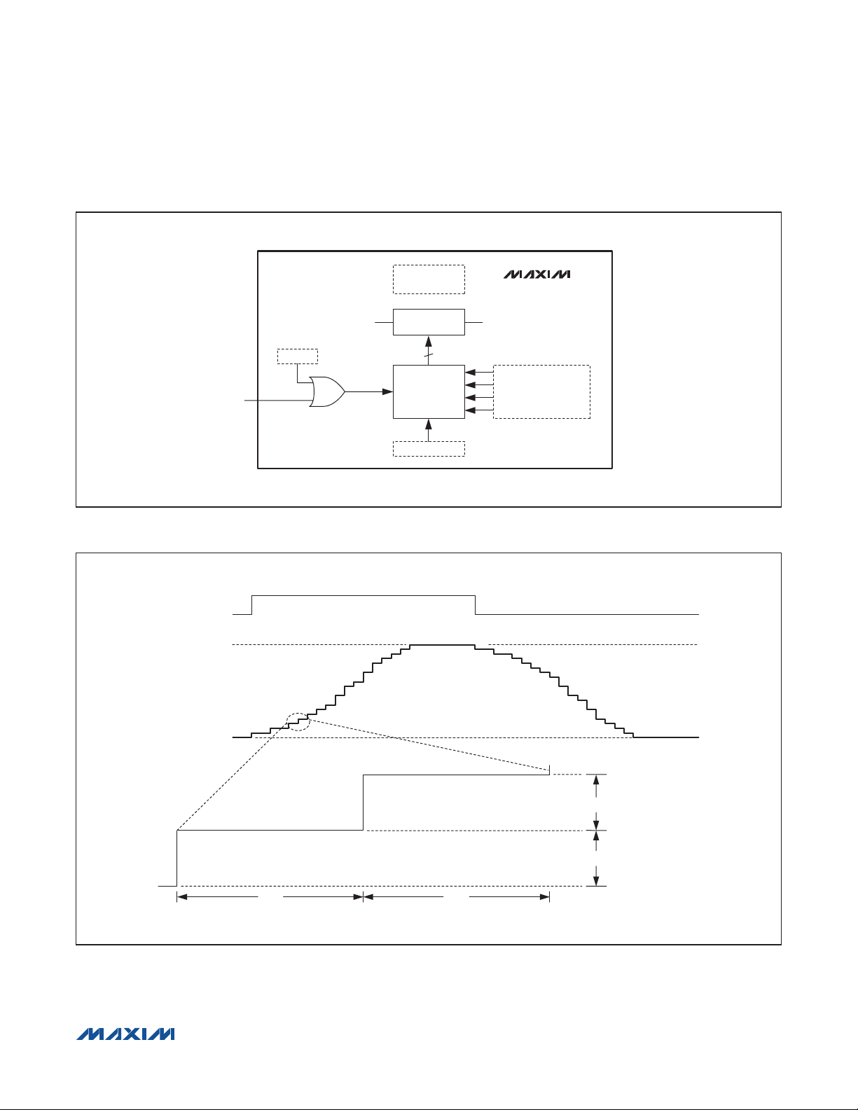
MAX7049
High-Performance, 288MHz to 945MHz
ASK/FSK ISM Transmitter
PROGRAMMABLE
CONTROL BITS
MAX7049
1621DATAIN
Figure 16. Tx FSK Mode Programming
Datain
base1[20:0]
datain
FROM VCO TO PFD
Datain
FRACTIONAL-N
DIVIDER D
FREQUENCY
WAVESHAPING
FUNCTION
base[20:0]
wsoff
shpnn[7:0] : nn = 00:18
wsmlt[1:0]
tstep[7:0]
base[20:0] → SPACE FREQUENCY
base1[20:0] → MARK FREQUENCY
base[20:0]
t
STEP
Figure 17. Tx FSK Frequency Waveshaping Timing Diagram
���������������������������������������������������������������� Maxim Integrated Products 28
t
STEP
shp05[7:0]
shp04[7:0]
Page 29

MAX7049
High-Performance, 288MHz to 945MHz
ASK/FSK ISM Transmitter
The 21-bit divider word is updated at a rate defined by
the tstep[7:0] bits, and this update time step is given by:
t
= tstep[7:0]/mclk
STEP
In terms of the shpnn[7:0] bits, the value of base1[20:0]
is therefore:
nn 18
/
=
∑
nn 00
=
16
nn 18
=
∑
nn 00
=
16
16
or
base1[20:0] base[20:0] shpnn[7:0]
As Figure 17 illustrates, the frequency ramp-down shape
is the inverse, not the mirror image, of the frequency
ramp-up shape. The frequency deviation, which is the
difference between the mark frequency and the space
frequency, can also be expressed in terms of the
shpnn[7:0] bits:
frequency deviation f 2 shpnn[7:0]
The waveshaping function allows for the approximation of
any monotonic-shape characteristic. An example of the
waveshaping function is the approximation of a 2kbps
NRZ with linear ramp shaping of duration at a 1/2 bit
interval and deviation of 50kHz. The length of the ramp
time is 250Fs. With a 3.2MHz mclk, a decimal value of
40 (0x28) is required for the tstep[7:0] SPI bits because
each of the time steps would need to be 12.5Fs, and 40
x 0.3125Fs yields 12.5Fs. This requires a decimal value
of 11 (0xB) for the shpnn[7:0] bits if used with a 16MHz
crystal. In this case the deviation is 19 (# of frequency
steps) x 11 (frequency change per step) x 16,000,000/2
or 51.03kHz. To attain a value closer to 50kHz at the
expense of linearity, four of the Shape00–Shape18
register values could have been set to decimal 10 (0xA).
This results in a deviation of 205 x 16,000,000/2
50.05kHz. The maximum programmable deviation (not
= +
= ×
XTAL
typically used with companion receivers due to bandwidth limitations) in this mode with a 16.0MHz crystal is
19 x 255 x 16,000,000/2
In this mode, the wsoff bit (TxConf0 register, 0x0C, bit 6)
is set and the wsmlt[1:0] bits (TxConf1 register, 0x0D,
bits 7:6) are used to transition directly from the space
frequency to the mark frequency without the use of
shaping. The value of base1[20:0] is expressed as:
base1[20:0] base[20:0] wsm shp00[7:0]= + ×
where wsm is a multiplier whose value is given in Table 8.
This mode of pulsed FSK might offer slightly better range
when compared to shaped FSK at the expense of a higher
occupied bandwidth. A waveshaping function is also
available in Tx ASK mode. This feature is documented in
the Power Amplifier section.
The required loop bandwidth of the fractional-N synthesizer is dependent on the required phase noise characteristics of the transmitted carrier signals, the required
frequency settling times, the FSK modulation rates, and
the current consumption.
Three components dominate the phase noise of the
fractional-N synthesizer output: close-in phase noise, VCO
phase noise, and fractional quantization phase noise.
The loop bandwidth and filter order can be set to meet
the requirements for a wide range of applications due to
the low close-in phase noise (for excellent performance
at wide-loop bandwidths) and low VCO phase noise
(for excellent performance at narrow-loop bandwidths).
The loop filter order can be increased to lessen the
effect of fractional quantization phase noise for wide-loop
bandwidths if necessary.
16
or 1.18MHz.
Tx Pulse FSK Mode
Loop Bandwidth
Table 8. Tx FSK Pulse Mode Frequency Multiplier Values
wsmlt[1:0] TxConf1 REGISTER, ADDRESS 0x0D, BITS 7:6 wsm
00 1
01 2
10 4
11 8
���������������������������������������������������������������� Maxim Integrated Products 29
Page 30
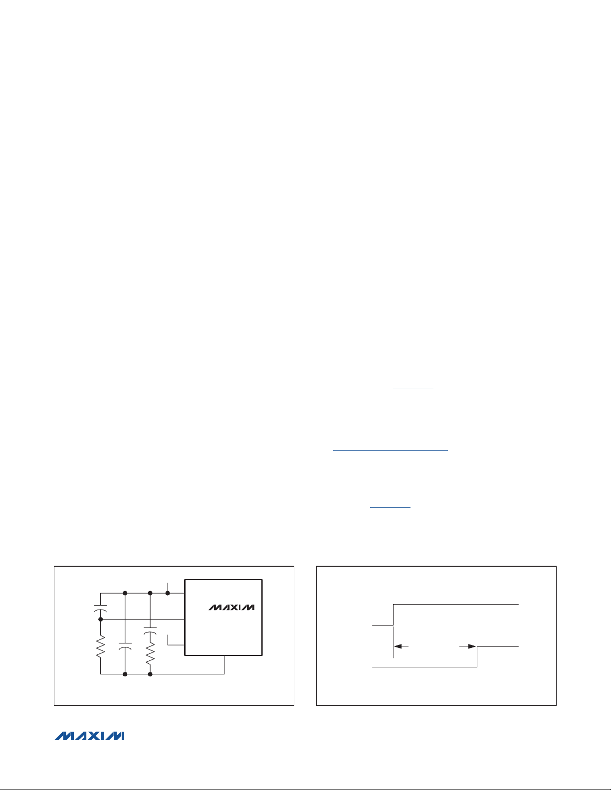
MAX7049
High-Performance, 288MHz to 945MHz
ASK/FSK ISM Transmitter
Generally, a 100kHz loop bandwidth works for most
applications. This choice allows for fast settling times,
within typically 48Fs for less than 5kHz offset during a
26MHz step in the 902MHz to 928MHz ISM band. This
loop bandwidth is near the optimum for minimizing the
contributions of both close-in phase noise and VCO
phase noise. In addition, this choice allows for FSK
modulation rates up to 160kbps NRZ and 80kbps
Manchester for most applications. If the phase noise at
higher offset frequencies needs to be reduced, the loop
bandwidth can be lowered to allow for the VCO noise to
dominate the phase-noise profile completely.
The loop filter components can be calculated as follows:
R = (2 x G x D x BW)/(ICP x K
VCO
)I
where:
R is the loop filter resistor in I.
D is the frequency division ratio of the feedback
divider of the fractional-N synthesizer.
BW is the desired fractional-N synthesizer loop bandwidth in Hz.
ICP is the charge-pump current in A.
K
is the VCO gain at the synthesizer output
VCO
frequency (863MHz to 945MHz) in Hz/V.
CL = (√10)/(2 x G x R x BW) in F
where:
CL is the large-loop filter capacitor in series with R.
R is the loop filter resistor in I.
BW is the desired fractional-N synthesizer loop bandwidth in Hz.
The value of 10 is approximate.
CS = 1/(2 x G x R x BW x (√10) ) in F
where:
CS is the small-loop filter capacitor in parallel with the
series combination of R and CL.
R is the loop filter resistor in I.
BW is the desired fractional-N synthesizer loop bandwidth in Hz.
The value of 10 is approximate.
An additional RC pole can be added to the loop filter
to remove more fractional quantization phase noise at
wide-loop bandwidths. This pole is added between the
CPOUT pin and the CTRL pin. The resistance of the RC
pole should be 1.5x the value of the loop filter resistor to
limit loading while minimizing thermal noise as a phasenoise contributor. The pole frequency should be greater
than ten times the loop bandwidth. The loop filter configuration is shown in Figure 18.
Lock Detector
The primary support circuit for the fractional-N synthesizer is the lock detector. The internal lock-detect
signal is a gate for transmitter operation as illustrated in
the Operating Mode Overview section. The lock-detect
signal itself is adequate for most operating conditions,
but additional delay can be added if this signal is asserted too quickly, such that it does not allow the synthesizer
to settle to within the desired frequency accuracy as
illustrated in Figure 19.
V
DD
5
VCOVDD
C
P
C
L
C
S
R
P
SHORT R
BYPASS V
Figure 18. Synthesizer Loop Filter Topology Figure 19. Lock Detector Delay Function
R
AND CP IF EXTRA POLE IS NOT USED.
P
AND C
COVDD
���������������������������������������������������������������� Maxim Integrated Products 30
V
DD
TO GROUND.
PVDD
6
7
CTRL
CPVDD
MAX7049
CPOUT
8
lockdet
plldel INTERVAL
plllock
Page 31

MAX7049
High-Performance, 288MHz to 945MHz
ASK/FSK ISM Transmitter
The additional delay interval is set by the plldl[2:0] bits
(Conf1 register, 0x02, bits 5:3), and this delay is given by:
plldel interval = plldl[2:0] x (64/mclk)s
where plldl[2:0] is the decimal equivalent of the bits, yielding a norminal (3.2MHz mclk) plldel interval from 0 to 140Fs.
Both the lockdet and plllock status signals are available
on SDO, GPO1, and GPO2, as described in the Register
Details section for the TestBus0 and TestBus1 registers.
Power Amplifier
The IC contains a programmable current-drain, highefficiency power amplifier (PA). The PA is a differential
output stage capable of delivering more than +15dBm to
a 50I load including the losses of the matching network
and harmonic filter. The bias current for the PA (IPA) is
configurable in 64 linear steps, as illustrated in Figure 20.
An external resistor (R
) is placed between the REXTPA
EXT
pin and ground. This resistor, along with an on-chip
reference voltage of 1.13V, sets the reference
current (IR). This resistor should be placed as close as
V
DD
possible to the IC to minimize the capacitance on this node.
A temperature-stable, high-tolerance ±1% resistor is
recommended to minimize variations in output power. An
on-chip current multiplier of 25 x IR determines the LSB
of the PA bias DAC. For example, a 56.2kI resistor sets
the LSB to 0.5mA. The palopwr bit (TxConf0 register,
0x0C, bit 7) controls the bias current in the PA buffer
amplifier. When this bit is set, it lowers the buffer bias
current by 2mA for low-power applications. The buffer
amplifier sets the pedestal voltage (VP), which is required
for sufficient PA bias DAC headroom.
The function of the matching network is to transform the
load resistance (RL) to the differential optimal PA load
resistance (R
). The value of R
OPT
is determined by
OPT
the desired output power (PD), the loss of the matching
network (Lm), the supply voltage (VDD), and the pedestal voltage (VP). Table 9 illustrates a design example for
determining R
and IPA_peak, where IPA_peak is the
OPT
peak value of the DC current.
L
J
28
FROM FREQUENCY
SYNTHESIZER
vi
REXTPA
2
1.13V
R
IR
EXT
BUFFER
AMP
CURRENT MIRROR
25x
I_lsb = 25 x IR
PA-
R
OPT
V
P
PA BIAS DAC
palopwr
IPA = (0:63)
x I_lsb
Figure 20. Power Amplifier Topology and Optimum Signal Swings
���������������������������������������������������������������� Maxim Integrated Products 31
INSERTION LOSS
= Lm
MATCHING
NETWORK
27
PA+
MAX7049
DIGITAL
CONTROL
6
R
L
(PA+) - (PA-)
SIGNAL SWINGS FOR
OPTIMAL LOAD
IMPEDANCE
vi 0
PA+
PA-
V
V
V
V
2 x (
0
DD
P
DD
P
V
- VP)
DD
Page 32

MAX7049
High-Performance, 288MHz to 945MHz
ASK/FSK ISM Transmitter
The maximum efficiency of an ideal differential output
stage is 2/G and this must also be adjusted by the factor
(VDD - VP)/VDD to account for the headroom required
for the PA bias DAC current source. Note that an unbalanced differential impedance, as seen by the PA output
pins, causes different clipping levels for the PA+ pin
vs. the PA- pin. This degrades efficiency. In addition, if
the matching network does not transform the load resis-
tance to a differential impedance whose value is exactly
R
+ j0, then this mismatch loss further degrades the
OPT
efficiency. In this PA design example, if the PA bias current
switched from zero to IPA_peak with the data input in ASK
mode, the occupied bandwidth of the modulated signal
would be significant. The IC includes an amplitude waveshaping function to reduce the occupied bandwidth of ASK
modulation.
Table 9. PA Design Example
PARAMETER SYMBOL AND/OR EQUATION EXAMPLE VALUE
Supply Voltage V
Pedestal Voltage V
External PA Bias Resistance R
PA Bias DAC LSB I_lsb = 25 x 1.13/R
Desired Peak RF Output Power P
Harmonic Filter and Composite
Matching/Combiner Network Loss
DD
P
EXT
EXT
D
Lm 2dB
Actual PA RF Output Power PPA = PL + Lm 16dBm
Actual PA RF Output Power PPA_mW = 10
Required PA DC Power
Maximum PA Efficiency
Composite PA Efficiency (includes
Matching Network Loss)
PDC = PPA_mW x G/2 x VDD/(VDD -VP)
Maximum efficiency = 100 x 2/G x (VDD - VP)/V
Efficiency = 100 x 10
Required Peak DC Current IPA_peak = PDC/V
(PPA/10)
(PD/10)
DD
DD
/P
DC
PA Code for Desired Power idac_peak[5:0] 50 decimal (0x32)
3V
0.5V
56.2kI
0.5mA
14dBm
40mW
75mW
53%
33%
25mA
16 DAT AIN
Figure 21. Tx ASK Mode Programming
���������������������������������������������������������������� Maxim Integrated Products 32
FROM FREQUENCY
SYNTHESIZER
vi
datain
PROGRAMMABLE
CONTROL BITS
BUFFER
AMP
MAX7049
Datain
idac[5:0]
6
AMPLITUDE
WAVESHAPING
FUNCTION
28
PA-
27
PA+
IPA = idac[5:0] x I_lsb
wsoff
shpnn[7:0] : nn = 00:18
wsmlt[1:0]
tstep[7:0]
Page 33

MAX7049
High-Performance, 288MHz to 945MHz
ASK/FSK ISM Transmitter
Tx ASK Mode Using Amplitude Waveshaping
The ASK waveshaping function is illustrated in Figure 21.
In this mode, the wsoff bit (TxConf0 register, 0x0C, bit 6)
is cleared and the wsmlt[1:0] bits (TxConf1 register,
0x0D, bits 7:6) are cleared. After txready is high, the PA
transitions from zero bias current to IPA_peak, on the
rising edge of the Datain signal. This transition occurs
in 20 discrete steps, determined by the tstep[7:0] bits
(TxTstep register, 0x0E, bits 7:0) and the shpnn[7:0] bits
(Shape00–Shape18 registers, 0x0F–0x21, bits 7:0, where
nn = 00 to 18), as shown in Figure 22.
The PA DAC word is updated at a rate defined by the
tstep[7:0] bits, and this update time step is given by:
t
= tstep[7:0]/mclk
STEP
In terms of the shpnn[7:0] bits, the value of idac_peak[5:0]
is therefore:
.
idac_peak[5:0] shpnn[7:0]
Datain
nn 18
=
nn 00
=
∑
=
The two most-significant bits of shpnn[7:0] should always
be zero in ASK mode. As Figure 22 illustrates, the rampdown shape is the inverse of the ramp-up shape. The
waveshaping function allows for the approximation of
any monotonic shape characteristic. Since the shpnn
registers are 8 bits wide, the PA can be pulsed from zero
current to the maximum bias current in one time step if
desired.
An example is the approximation of a 4kbps NRZ with
linear ramp shaping of 1/2 bit interval duration and
peak PA bias current of 10mA using R
= 56.2kI.
EXT
The length of the ramp time is 125Fs. With a 3.2MHz
mclk, this requires a decimal value of 20 (0x14) for the
tstep[7:0] because each of the 20 time steps would need
to be 6.25Fs, and 20 x 0.3125Fs yields 6.25Fs. This
requires a decimal value of 1 (0x1) for each Shape00–
Shape18 register. In this case, the peak PA bias current
is 19 x 25 x 1.13/56,200, or 9.55mA. To attain a value
closer to 10mA at the expense of linearity, one of the
Shape00–Shape18 register values could have been set
to decimal 2 (0x2). This results in a peak PA bias current
of 20 x 25 x 1.13/56,200, or 10.05mA.
idac_peak[5:0]
0
t
STEP
Figure 22. ASK Waveshaping Timing Diagram
���������������������������������������������������������������� Maxim Integrated Products 33
t
STEP
shp05[7:0]
shp04[7:0]
Page 34

MAX7049
High-Performance, 288MHz to 945MHz
ASK/FSK ISM Transmitter
Tx FSK Mode Amplitude Ramp
In Tx FSK mode, the carrier is modulated by the
frequency-shaping function, as defined in the Fractional-N
Synthesizer section. This frequency waveshaping is
designed to minimize the occupied bandwidth of the
transmit signal in Tx FSK mode. However, the occupied
bandwidth might degrade if the PA turns on and off
abruptly at the beginning and end of a burst. A PA amplitude ramp feature is available in Tx FSK mode to prevent
the degradation of the occupied bandwidth. This feature
is illustrated in Figure 23.
After the IC is enabled and the txready signal transitions high, the PA bias current ramps up linearly to the
value fska[5:0] (TxConf0 register, 0x0C, bits 5:0) x I_lsb
in increments of fskas[5:0] (TxConf1 register, 0x0D, bits
5:0) x I_lsb, as illustrated in Figure 24.
FROM FREQUENCY
SYNTHESIZER
vi
BUFFER
AMP
Similarly, the PA bias current ramps down linearly on
the falling edge of the enable signal. Note that this PA
ramp feature is also automatically invoked when hopping
from one channel to another channel, as defined in the
Fractional-N Synthesizer section.
The PA DAC word is updated at a rate defined by the
tstep[7:0] bits, and this update time step is given by:
t
= tstep[7:0]/mclk
STEP
To transmit the entire message at the desired power
level, the user should wait until the PA ramp is completed
before initiating the data sequence.
28
PA-
27
PA+
enable
ENABLE
17
Figure 23. Tx FSK Amplitude Ramp Feature
���������������������������������������������������������������� Maxim Integrated Products 34
MAX7049
PROGRAMMABLE
CONTROL BITS
Enable
idac[5:0]
6
AMPLITUDE
RAMP
FUNCTION
IPA = idac[5:0] x I_lsb
fska[5:0]
fskas[5:0]
tstep[7:0]
Page 35

enable AND
txready
fska[5:0]
MAX7049
High-Performance, 288MHz to 945MHz
ASK/FSK ISM Transmitter
0
fskas[5:0]
fskas[5:0]
t
STEP
Figure 24. Tx FSK Amplitude Ramp Timing Diagram
t
STEP
Register Details
Table 10. Configuration Register Map
GROUP/FUNCTION HEX BIT 7 BIT 6 BIT 5 BIT 4 BIT 3 BIT 2 BIT 1 BIT 0
0 Ident 0x00 1 0 1 0 0 1 1 1
1
2
3
4
Conf0 0x01 — — — mode fsel_1 fsel_0 xtal_1 xtal_0
Conf1 0x02 icont ibsel plldl_2 plldl_1 plldl_0 — — —
IOConf0 0x03 gp1isht gp2isht ckdiv_1 ckdiv_0 gp2s_3 gp2s_2 gp2s_1 gp2s_0
IOConf1 0x04 sdos_3 sdos_2 sdos_1 sdos_0 gp1s_3 gp1s_2 gp1s_1 gp1s_0
IOConf2 0x05 — — gp1md_1 gp1md_0 clksht gp2md_2 gp2md_1 gp2md_0
FBase0 0x08 — — — base_20 base_19 base_18 base_17 base_16
FBase1 0x09 base_15 base_14 base_13 base_12 base_11 base_10 base_9 base_8
FBase2 0x0A base_7 base_6 base_5 base_4 base_3 base_2 base_1 base_0
FLoad 0x0B — — — — — — — hop
TxConf0 0x0C palopwr wsoff fska_5 fska_4 fska_3 fska_2 fska_1 fska_0
TxConf1 0x0D wsmlt_1 wsmlt_0 fskas_5 fskas_4 fskas_3 fskas_2 fskas_1 fskas_0
TxTstep 0x0E tstep_7 tstep_6 tstep_5 tstep_4 tstep_3 tstep_2 tstep_1 tstep_0
���������������������������������������������������������������� Maxim Integrated Products 35
Page 36

MAX7049
High-Performance, 288MHz to 945MHz
ASK/FSK ISM Transmitter
Table 10. Configuration Register Map (continued)
GROUP/FUNCTION HEX BIT 7 BIT 6 BIT 5 BIT 4 BIT 3 BIT 2 BIT 1 BIT 0
Shape00 0x0F shp00_7 shp00_6 shp00_5 shp00_4 shp00_3 shp00_2 shp00_1 shp00_0
Shape01 0x10 shp01_7 shp01_6 shp01_5 shp01_4 shp01_3 shp01_2 shp01_1 shp01_0
Shape02 0x11 shp02_7 shp02_6 shp02_5 shp02_4 shp02_3 shp02_2 shp02_1 shp02_0
Shape03 0x12 shp03_7 shp03_6 shp03_5 shp03_4 shp03_3 shp03_2 shp03_1 shp03_0
Shape04 0x13 shp04_7 shp04_6 shp04_5 shp04_4 shp04_3 shp04_2 shp04_1 shp04_0
Shape05 0x14 shp05_7 shp05_6 shp05_5 shp05_4 shp05_3 shp05_2 shp05_1 shp05_0
Shape06 0x15 shp06_7 shp06_6 shp06_5 shp06_4 shp06_3 shp06_2 shp06_1 shp06_0
Shape07 0x16 shp07_7 shp07_6 shp07_5 shp07_4 shp07_3 shp07_2 shp07_1 shp07_0
Shape08 0x17 shp08_7 shp08_6 shp08_5 shp08_4 shp08_3 shp08_2 shp08_1 shp08_0
5
Shape09 0x18 shp09_7 shp09_6 shp09_5 shp09_4 shp09_3 shp09_2 shp09_1 shp09_0
Shape10 0x19 shp10_7 shp10_6 shp10_5 shp10_4 shp10_3 shp10_2 shp10_1 shp10_0
Shape11 0x1A shp11_7 shp11_6 shp11_5 shp11_4 shp11_3 shp11_2 shp11_1 shp11_0
Shape12 0x1B shp12_7 shp12_6 shp12_5 shp12_4 shp12_3 shp12_2 shp12_1 shp12_0
Shape13 0x1C shp13_7 shp13_6 shp13_5 shp13_4 shp13_3 shp13_2 shp13_1 shp13_0
Shape14 0x1D shp14_7 shp14_6 shp14_5 shp14_4 shp14_3 shp14_2 shp14_1 shp14_0
Shape15 0x1E shp15_7 shp15_6 shp15_5 shp15_4 shp15_3 shp15_2 shp15_1 shp15_0
Shape16 0x1F shp16_7 shp16_6 shp16_5 shp16_4 shp16_3 shp16_2 shp16_1 shp16_0
Shape17 0x20 shp17_7 shp17_6 shp17_5 shp17_4 shp17_3 shp17_2 shp17_1 shp17_0
Shape18 0x21 shp18_7 shp18_6 shp18_5 shp18_4 shp18_3 shp18_2 shp18_1 shp18_0
TestMux 0x3C — — — — tmux_3 tmux_2 tmux_1 tmux_0
6
7
“—” Denotes a reserved bit. If a register contains reserved bits, write 0 to the reserved bit content.
Register 0x00 contents are always 0xA7, and can be used to identify the IC on the SPI bus.
Registers 0x40 through 0x43 are read-only registers, containing various states and status that can be read through the SPI.
Datain 0x3D — datain — — — — — —
EnableReg 0x3E — — — — tsensor — — enable
TestBus0 0x40 tbus_15 tbus_14 tbus_13 tbus_12 tbus_11 tbus_10 tbus_9 tbus_8
TestBus1 0x41 tbus_7 tbus_6 tbus_5 tbus_4 tbus_3 tbus_2 tbus_1 tbus_0
Status0 0x42 txready — adcrdy — gpo1out plllock lockdet ckalive
Status1 0x43 — — — tsdone — — — —
���������������������������������������������������������������� Maxim Integrated Products 36
Page 37

MAX7049
High-Performance, 288MHz to 945MHz
ASK/FSK ISM Transmitter
Detailed Register Descriptions
Table 11. Group 0: Identification Register (Ident)
GROUP/FUNCTION HEX BIT 7 BIT 6 BIT 5 BIT 4 BIT 3 BIT 2 BIT 1 BIT 0
0 Ident 0x00 1 0 1 0 0 1 1 1
Table 12. Ident Register (0x00)
BIT NAME FUNCTION
7:0 ident[7:0] Read-only register used for identification purposes. The content of this register is always 0xA7.
Table 13. Group 1: General Configuration Registers (Conf0, Conf1)
GROUP/FUNCTION HEX BIT 7 BIT 6 BIT 5 BIT 4 BIT 3 BIT 2 BIT 1 BIT 0
1
Conf0 0x01 — — — mode fsel_1 fsel_0 xtal_1 xtal_0
Conf1 0x02 icont ibsel plldl_2 plldl_1 plldl_0 — — —
Table 14. Conf0 Register (0x01)
BIT NAME FUNCTION
1-bit configuration for transmit mode:
4 mode
3:2 fsel[1:0]
1:0 xtal[1:0]
0 = ASK
1 = FSK
2-bit configuration for LO division ratio:
00 3
01 2
10 Not used
11 1
2-bit crystal divider configuration. Based on a typical crystal selection of 16.0MHz, 19.2MHz, or
22.4MHz, these bits are usually configured to yield a constant 3.2MHz mclk frequency for timing
control and driving characteristics of the digital section of the IC. For data rates up to 200kbps,
an mclk frequency of up to 4.0MHz is needed. The typical settings are:
Crystal xtal[1:0]
16.0MHz 00 Divide by 5 (16.0/5 = 3.2MHz)
19.2MHz 01 Divide by 6 (19.2/6 = 3.2MHz)
22.4MHz 10 Divide by 7 (22.4/7 = 3.2MHz)
20.0MHz 00 Divide by 5 (20.0/5 = 4.0MHz)
11 Divide by 8
���������������������������������������������������������������� Maxim Integrated Products 37
Page 38

High-Performance, 288MHz to 945MHz
ASK/FSK ISM Transmitter
Table 15. Conf1 Register (0x02)
BIT NAME FUNCTION
7 icont
6 ibsel
5-3 plldl[2:0]
Selects between low current (0 = 204FA) and high current (1 = 407FA) modes for the synthesizer
charge pump, allowing for lower noise operation with the expense of extra current.
Selects between low VCO core current and high VCO core current (1 = additional 1mA) in the
synthesizer.
3-bit configuration for extra delay after lock-detect flag (lockdet) from the synthesizer is asserted
(assuming mclk = 3.2MHz):
plldl[2:0] delay(Fs)
000 0
001 20
010 40
011 60
100 80
101 100
110 120
111 140
After this delay, an internal signal called plllock is asserted high to determine the digital lock flag
for the synthesizer.
MAX7049
Table 16. Group 2: GPO, Data Output, and Clock Output Registers
(IOConf0, IOConf1, IOConf2)
GROUP/FUNCTION HEX BIT 7 BIT 6 BIT 5 BIT 4 BIT 3 BIT 2 BIT 1 BIT 0
IOConf0 0x03 gp1isht gp2isht ckdiv_1 ckdiv_0 gp2s_3 gp2s_2 gps2_1 gps2_0
2
IOConf1 0x04 sdos_3 sdos_2 sdos_1 sdos_0 gp1s_3 gp1s_2 gp1s_1 gp1s_0
IOConf2 0x05 — — gp1md_1 gp1md_0 clksht gp2md_2 gp2md_1 gp2md_0
���������������������������������������������������������������� Maxim Integrated Products 38
Page 39

High-Performance, 288MHz to 945MHz
ASK/FSK ISM Transmitter
Table 17. IOConf0 Register (0x03)
BIT NAME FUNCTION
GPO1 current mode during sleep. If the IC GPO1 is configured to current drive mode (IOConf2
7 gp1isht
6 gp2isht
5:4 ckdiv[1:0]
3:0 gp2s[3:0]
register, 0x05), writing 1 to this bit allows for the current mode operation even if the IC is in Sleep
mode or disabled. If this bit is 0, current mode operation is only active when the IC is enabled.
GPO2 current mode during sleep. If the IC GPO2 is configured to current drive mode (IOConf2
register, 0x05), writing 1 to this bit allows for the current mode operation even if the IC is in Sleep
mode or disabled. If this bit is 0, current mode operation is only active when the IC is enabled.
2-bit configuration for clock output divider setting. A clock source selected by gp2s[3:0] is divided by
the settings in these bits, according to the following:
ckdiv[1:0] Divide by
00 1
01 2
10 4
11 8
4-bit configuration for GPO2 signal selection:
gp2s[3:0] Output
0000 plllock
0001 mclk/(ckdiv divider)
0010 xtal/(ckdiv divider)
0011 xtal/16/(ckdiv divider)
0100 tbus[4]
0101 tbus[5]
0110 tbus[6]
0111 tbus[7]
1000 tbus[8]
1001 tbus[9]
1011 tbus[10]
1100 tbus[11]
1101 tbus[12]
1110 tbus[14]
1111 tbus[15]
where:
mclk is the master digital clock generated from the crystal divider block (xtal[1:0]);
xtal is the crystal oscillator output clock;
xtal/16 is a divided-by-16 version of the crystal oscillator frequency;
tbus[15:0] is the 16-bit bus selected by tmux[3:0] (TestMux register, 0x3C, bits 3:0).
MAX7049
���������������������������������������������������������������� Maxim Integrated Products 39
Page 40

High-Performance, 288MHz to 945MHz
ASK/FSK ISM Transmitter
Table 18. Register IOConf1 (0x04)
BIT NAME FUNCTION
4-bit SPI data output GPO mode selection. When CS is low, the SDO pin outputs the SPI data output,
as described in the Serial Peripheral Interface (SPI) section. When CS is high, the SDO acts as a third
GPO, according to:
CS sdos[3] sdos[2] sdos[1] sdos[0] output
0 x x x x SPI_Dout
1 0 0 0 0 tbus[ 0]
1 0 0 0 1 tbus[ 1]
1 0 0 1 0 tbus[ 2]
1 0 0 1 1 tbus[ 3]
1 0 1 0 0 tbus[ 4]
7:4 sdos[3:0]
1 0 1 0 1 tbus[ 5]
1 0 1 1 0 tbus[ 6]
1 0 1 1 1 tbus[ 7]
1 1 0 0 0 tbus[ 8]
1 1 0 0 1 tbus[ 9]
1 1 0 1 0 tbus[10]
1 1 0 1 1 tbus[11]
1 1 1 0 0 tbus[12]
1 1 1 0 1 tbus[13]
1 1 1 1 0 tbus[14]
1 1 1 1 1 tbus[15]
tbus[15:0] is the 16-bit bus selected by tmux[3:0] (TestMux register, 0x3C, bits 3:0).
MAX7049
3:0 gp1s[3:0]
���������������������������������������������������������������� Maxim Integrated Products 40
4-bit configuration for GPO1 signal selection:
gp1s[3] gp1s[2] gp1s[1] gp1s[0] output
0 0 0 0 tbus[ 0]
0 0 0 1 tbus[ 1]
0 0 1 0 tbus[ 2]
0 0 1 1 tbus[ 3]
0 1 0 0 tbus[ 4]
0 1 0 1 tbus[ 5]
0 1 1 0 tbus[ 6]
0 1 1 1 tbus[ 7]
1 0 0 0 tbus[ 8]
1 0 0 1 tbus[ 9]
1 0 1 0 tbus[10]
1 0 1 1 tbus[11]
1 1 0 0 tbus[12]
1 1 0 1 tbus[13]
1 1 1 0 tbus[14]
1 1 1 1 tbus[15]
tbus[15:0] is the 16-bit bus selected by tmux[3:0] (TestMux register, 0x3C, bits 3:0).
Page 41

MAX7049
High-Performance, 288MHz to 945MHz
ASK/FSK ISM Transmitter
Table 19. Register IOConf2 (0x05)
BIT NAME FUNCTION
2-bit GPO1 mode selection:
5:4 gp1md[1:0]
3 clksht Enable (1) or disable (0) clock output on GPO2 during sleep.
2:0 gp2md[2:0]
Table 20. Group 3: Synthesizer Frequency Settings (FBase0, FBase1, FBase2, FLoad)
0x buffer mode
10 80FA current mode
11 160FA current mode
3-bit GPO2 mode selection. The GPO2 can provide a high-frequency clock output, and therefore its
current capability is higher.
0xx buffer mode
100 1.0mA
101 2.0mA
110 3.0mA
111 4.0mA
GROUP/FUNCTION HEX BIT 7 BIT 6 BIT 5 BIT 4 BIT 3 BIT 2 BIT 1 BIT 0
FBase0 0x08 — — — base_20 base_19 base_18 base_17 base_16
3
Registers 0x08, 0x09, and 0x0A set the 21-bit base value for the control of the synthesizer frequency. Bits 20:16 form
the 5-bit integer part (base[20:16]), and bits 15:0 form the 16-bit fractional part (base[15:0]).
The synthesizer frequency is then given by:
where f
settings (Conf0 register, 0x01, bits 3:2) to generate the LO frequency:
FBase1 0x09 base_15 base_14 base_13 base_12 base_11 base_10 base_9 base_8
FBase2 0x0A base_7 base_6 base_5 base_4 base_3 base_2 base_1 base_0
FLoad 0x0B — — — — — — — hop
f
is the crystal frequency in MHz. The synthesizer frequency is then divided according to the fsel[1:0]
XTAL
SYNTH
= f
x (32 + base[20:0]/65,536)
L
XTA
Table 21. Synthesizer Divider Settings
fsel[1:0] LO DIVIDER
00 3
01 2
11 1
���������������������������������������������������������������� Maxim Integrated Products 41
Page 42

MAX7049
High-Performance, 288MHz to 945MHz
ASK/FSK ISM Transmitter
The synthesizer frequency range is from 863MHz to 945MHz, which translates to the base[20:0] values shown in Table 22.
Table 22. Synthesizer Programming Values
CRYSTAL (MHz) SYNTHF (MHz) MULTIPLIER FACTOR (dec) base[20:0]
16.0
19.2
22.4
20
The minimum and maximum frequency for each band is shown in Table 23.
Table 23. Frequency Ranges
863 21.9375 0x15F000
945 27.0625 0x1B1000
863 12.9479 0x0CF2AB
945 17.2188 0x113800
863 6.5268 0x0686DB
945 10.1875 0x0A3000
863 11.1500 0x0B2666
945 15.2500 0x0F4000
SYNTHF (MHz)
863 287.70 431.50 863.00
945 315.00 472.50 945.00
The hop bit allows for a parallel load of the three FBase registers. This is a self-reset bit that reverts to 0 when the operation is completed. This function can also be accomplished by use of the external HOP pin. A detailed description of the
hop operation can be found in the appropriate sections of the transmitter detailed operations descriptions.
300MHz (fsel = 00) 450MHz (fsel = 01) 900MHz (fsel = 11)
Table 24. FBase0 Register (0x08)
BIT NAME FUNCTION
4:0 base[20:16] 5-bit integer value for synthesizer.
Table 25. FBase1 Register (0x09)
BIT NAME FUNCTION
7:0 base[15:8] 8 MSBs of fractional value for synthesizer.
Table 26. FBase2 Register (0x0A)
BIT NAME FUNCTION
7:0 base[7:0] 8 LSBs of fractional value for synthesizer.
Table 27. FLoad (0x0B)
BIT NAME FUNCTION
0 hop
Hop bit. Loads the synthesizer fractional-N divider base value to base[20:0] written in registers
8 through 10. This is a self-reset bit, and is reset to zero after the operation is completed.
���������������������������������������������������������������� Maxim Integrated Products 42
Page 43

MAX7049
High-Performance, 288MHz to 945MHz
ASK/FSK ISM Transmitter
Table 28. Group 4: Transmiter Amplitude and Timing Parameters
(TxConf0, TxConf1, TxTstep)
GROUP/FUNCTION HEX BIT 7 BIT 6 BIT 5 BIT 4 BIT 3 BIT 2 BIT 1 BIT 0
TxConf0 0x0C palopwr wsoff fska_5 fska_4 fska_3 fska_2 fska_1 fska_0
4
These registers set general FSK/ASK parameters for PA amplitude and rate control (FSK), shaping control, and the step
control used for amplitude or frequency shaping.
Table 29. TxConf0 Register (0x0C)
TxConf1 0x0D wsmlt_1 wsmlt_0 fskas_5 fskas_4 fskas_3 fskas_2 fskas_1 fskas_0
TxTstep 0x0E tstep_7 tstep_6 tstep_5 tstep_4 tstep_3 tstep_2 tstep_1 tstep_0
BIT NAME FUNCTION
7 palopwr Reduces the PA input buffer current by 2mA when set to 1. Useful at low output power levels.
Disables (1) or enables (0) waveshaping. If waveshaping is disabled, only shp00[7:0] (Shape00
6 wsoff
5:0 fska[5:0] 6-bit final value for FSK PA amplitude (bias current) control.
register, 0x0F) and wsmlt[1:0] (TxConf1 register, 0x0D) are used to set the amplitude (ASK) or
frequency (FSK) deviation.
Table 30. TxConf1 Register (0x0D)
BIT NAME FUNCTION
2-bit scaler for shp00[7:0] (Shape00 register, 0x0F), effectively multiplying the value of Shape00 by:
wsmlt[1:0] multiplier
7:6 wsmlt[1:0]
5:0 fskas[5:0]
0 0 1
0 1 2
1 0 4
1 1 8
6-bit FSK amplitude (bias current) step for ramp-up and ramp-down operations. The PA amplitude
increases/decreases by this amount for every 1/20th of the data rate time elapsed (TxTstep register,
0x0E), until it reaches the final fska[5:0] value when ramping up, or reaches 0 when ramping down.
Table 31. TxTstep Register (0x0E)
BIT NAME FUNCTION
8-bit update value for waveshaping. This setting corresponds to 1/20th of the data rate, given in
periods of the master digital clock (312.5ns for 3.2 MHz).
tstep[7:0] = INT (mclk/(20 x DataRate))
For 80kbps < DataRate P 160kbps, tstep[7:0] = 1, mclk = 3.2MHz
7:0 tstep[7:0]
For 40kbps < DataRate P 80kbps, tstep[7:0] = 2, mclk = 3.2MHz
For 160kbps < DataRate P 200kbps, tstep[7:0] = 1, mclk = 4.0MHz
For 4kbps, tstep = INT (3.2 x10⁶/(20 x 4000)) = 40 (0x28), mclk = 3.2MHz
The maximum value for tstep[7:0] is 255, which allows for a minimum shaped data rate of 627bps.
These values assume shaping during the entire bit interval. The tstep value can be set lower if
possible for shaping during a portion of the bit interval.
This setting allows for the 20 sequential steps in either the amplitude (ASK) or frequency (FSK) waveshaping process,
for each symbol of the transmitted data.
���������������������������������������������������������������� Maxim Integrated Products 43
Page 44

MAX7049
High-Performance, 288MHz to 945MHz
ASK/FSK ISM Transmitter
Table 32. Group 5: Transmitter Shaping Registers (Shape00–Shape18)
GROUP/FUNCTION HEX BIT 7 BIT 6 BIT 5 BIT 4 BIT 3 BIT 2 BIT 1 BIT 0
Shape00 0x0F shp00_7 shp00_6 shp00_5 shp00_4 shp00_3 shp00_2 shp00_1 shp00_0
Shape01 0x10 shp01_7 shp01_6 shp01_5 shp01_4 shp01_3 shp01_2 shp01_1 shp01_0
Shape02 0x11 shp02_7 shp02_6 shp02_5 shp02_4 shp02_3 shp02_2 shp02_1 shp02_0
Shape03 0x12 shp03_7 shp03_6 shp03_5 shp03_4 shp03_3 shp03_2 shp03_1 shp03_0
Shape04 0x13 shp04_7 shp04_6 shp04_5 shp04_4 shp04_3 shp04_2 shp04_1 shp04_0
Shape05 0x14 shp05_7 shp05_6 shp05_5 shp05_4 shp05_3 shp05_2 shp05_1 shp05_0
Shape06 0x15 shp06_7 shp06_6 shp06_5 shp06_4 shp06_3 shp06_2 shp06_1 shp06_0
Shape07 0x16 shp07_7 shp07_6 shp07_5 shp07_4 shp07_3 shp07_2 shp07_1 shp07_0
Shape08 0x17 shp08_7 shp08_6 shp08_5 shp08_4 shp08_3 shp08_2 shp08_1 shp08_0
5
Shape09 0x18 shp09_7 shp09_6 shp09_5 shp09_4 shp09_3 shp09_2 shp09_1 shp09_0
Shape10 0x19 shp10_7 shp10_6 shp10_5 shp10_4 shp10_3 shp10_2 shp10_1 shp10_0
Shape11 0x1A shp11_7 shp11_6 shp11_5 shp11_4 shp11_3 shp11_2 shp11_1 shp11_0
Shape12 0x1B shp12_7 shp12_6 shp12_5 shp12_4 shp12_3 shp12_2 shp12_1 shp12_0
Shape13 0x1C shp13_7 shp13_6 shp13_5 shp13_4 shp13_3 shp13_2 shp13_1 shp13_0
Shape14 0x1D shp14_7 shp14_6 shp14_5 shp14_4 shp14_3 shp14_2 shp14_1 shp14_0
Shape15 0x1E shp15_7 shp15_6 shp15_5 shp15_4 shp15_3 shp15_2 shp15_1 shp15_0
Shape16 0x1F shp16_7 shp16_6 shp16_5 shp16_4 shp16_3 shp16_2 shp16_1 shp16_0
Shape17 0x20 shp17_7 shp17_6 shp17_5 shp17_4 shp17_3 shp17_2 shp17_1 shp17_0
Shape18 0x21 shp18_7 shp18_6 shp18_5 shp18_4 shp18_3 shp18_2 shp18_1 shp18_0
These registers set the amplitude (ASK) or frequency deviation (FSK) modulated by the incoming transmitted data.
For every 1/20th of the bit rate defined by tstep[7:0], the following shape value is added to the previous accumulated
result. All the shape values are deltas, and the final ASK amplitude or FSK deviation is given by the cumulative sum of
all the shape registers.
In ASK, the initial value is 0. For FSK, the initial value is given by base[20:0]. There are 20 intervals (hence 19 shape
registers) that are added on the 0-1 transition of the transmitted data or subtracted from on the 1-0 transition.
Table 33. Shape00 Register (0x0F)
BIT NAME FUNCTION
First 8-bit value for waveshaping. This value is effectively multiplied by the wsmlt[1:0] setting
7:0 shp00[7:0]
(TxConf1 register, 0x0D). If the wsoff bit is high, this is the only value that is added or subtracted to
perform either amplitude (ASK) or frequency (FSK) modulation.
���������������������������������������������������������������� Maxim Integrated Products 44
Page 45

High-Performance, 288MHz to 945MHz
ASK/FSK ISM Transmitter
Table 34. Shape01–Shape18 Registers (0x10–0x21)
BIT NAME FUNCTION
shp01[7:0]
shp02[7:0]
shp03[7:0]
shp04[7:0]
shp05[7:0]
shp06[7:0]
shp07[7:0]
7:0
shp08[7:0]
shp09[7:0]
shp10[7:0]
shp11[7:0]
shp12[7:0]
shp13[7:0]
shp14[7:0]
shp15[7:0]
shp16[7:0]
shp17[7:0]
shp18[7:0]
18 8-bit values for waveshaping. These values, along with shp00[7:0], yield the 19 different values
(20 intervals) used for waveshaping, one for each of the 20 updates occurring during each 0-1 or
1-0 transmitted data transition.
MAX7049
Table 35. Group 6: Control Registers (TestMux, Datain, EnableReg)
GROUP/FUNCTION HEX BIT 7 BIT 6 BIT 5 BIT 4 BIT 3 BIT 2 BIT 1 BIT 0
TestMux 0x3C — — — — tmux_3 tmux_2 tmux_1 tmux_0
6
Datain 0x3D — datain — — — — — —
EnableReg 0x3E — — — — tsensor — — enable
This register group combines status bus control (tbus[15:0]), GPO controls, temperature sensor control, register control
of pin function (txdata), and enable controls.
Table 36. TestMux Register (0x3C)
BIT NAME FUNCTION
4-bit selection of tbus[15:0] (TestBus0 and TestBus1 registers, 0x40 and 0x41) contents. See the
3:0 tmux[3:0]
TestBus0 and TestBus1 register descriptions for a complete description of what can be observed
through this 16-bit bus.
���������������������������������������������������������������� Maxim Integrated Products 45
Page 46

High-Performance, 288MHz to 945MHz
ASK/FSK ISM Transmitter
Table 37. Datain Register (0x3D)
BIT NAME FUNCTION
Transmit datain bit. This is a register equivalent of the DATAIN pin. When either the DATAIN pin or datain bit is 1,
6 datain
Table 38. EnableReg Register (0x3E)
BIT NAME FUNCTION
3 tsensor
0 enable
the transmit data is 1. Only when both are 0 the transmit data is 0 (logical OR function). Keep 0 if only the external DATAIN pin is used, and keep DATAIN pin 0 if the internal datain bit is used.
Writing a 1 to this bit starts the temperature sensor A/D conversion. This is a self-reset bit, where the
bit is automatically reset when the conversion is finished. The result can then be read through the
TestBus1 register (0x41). This function is available only in Sleep mode.
Enables (1) or disables (0) the IC’s transmitter operations. To enable the IC, SHDN must be driven low. This is a
register equivalent of the ENABLE pin. When either the ENABLE pin or enable bit is 1, the IC transmit operation
is enabled. Only when both are 0 the transmitter is disabled (logical-OR function). Keep 0 if only the external
ENABLE pin is used, and keep ENABLE pin 0 if the internal enable is used.
MAX7049
Table 39. Group 7: Read-Only Status Registers (TestBus0, TestBus1, Status0, Status1)
GROUP/FUNCTION HEX BIT 7 BIT 6 BIT 5 BIT 4 BIT 3 BIT 2 BIT 1 BIT 0
TestBus0 0x40 tbus_15 tbus_14 tbus_13 tbus_12 tbus_11 tbus_10 tbus_9 tbus_8
TestBus1 0x41 tbus_7 tbus_6 tbus_5 tbus_4 tbus_3 tbus_2 tbus_1 tbus_0
7
Registers 0x3F–0x43 are read-only registers used for A/D results, status, and test.
Status0 0x42 txready — adcrdy — gpo1out plllock lockdet ckalive
Status1 0x43 — — — tsdone — — — —
Table 40. TestBus0 Register (0x40)
BIT NAME FUNCTION
7:0 tbus[15:8] 8 MSBs of the internal 16-bit bus tbus[15:0], selected by tmux[3:0] (TextMux register, 0x3C, bits 3:0).
���������������������������������������������������������������� Maxim Integrated Products 46
Page 47
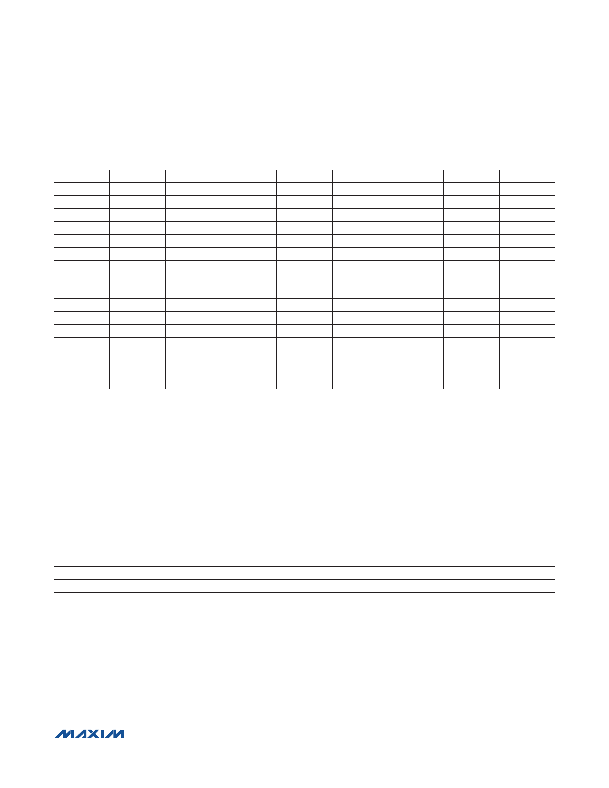
MAX7049
High-Performance, 288MHz to 945MHz
ASK/FSK ISM Transmitter
Table 41. Test Bus Signals (tbus[15:8])
tmux[3:0] tbus[15] tbus[14] tbus[13] tbus[12] tbus[11] tbus[10] tbus[9] tbus[8]
0x0 — — — — — — — —
0x1 — — — — — — — —
0x2 — — — — — — — —
0x3 — — — — — — — —
0x4 — — — — — — — —
0x5 — — pabia[5] pabia[4] pabia[3] pabia[2] pabia[1] pabia[0]
0x6 frac[15] frac[14] frac[13] frac[12] frac[11] frac[10] frac[9] frac[8]
0x7 — — — — — — — —
0x8 — — — — — — — —
0x9 — — — — — — — —
0xA — — — — — — — —
0xB — — — — — — — mclk
0xC — — — — — — — plllock
0xD — — — — — — — —
0xE — — — — — — — —
0xF — — — — — — — —
where:
tmux[3:0] Signal Description
0x0–0x4 — Reserved signals for test purposes
0x5 pabia[5:0] PA amplitude control bus
0x6 frac[15:8] MSBs of fractional value sent to frequency synthesizer
0x7–0xA — Reserved signals for test purposes
0xB mclk Master digital clock
0xC plllock Synthesizer lock signal
0xD–0xF — Reserved signals for test purposes
Table 42. TestBus1 Register (0x41)
BIT NAME FUNCTION
7:0 tbus[7:0] 8 LSBs of the internal 16-bit bus tbus[15:0], selected by tmux[3:0] (TestMux register, 0x3C, bits 3:0).
���������������������������������������������������������������� Maxim Integrated Products 47
Page 48

MAX7049
High-Performance, 288MHz to 945MHz
ASK/FSK ISM Transmitter
Table 43. Test Bus Signals (tbus[7:0])
tmux[3:0] tbus[7] tbus[6] tbus[5] tbus[4] tbus[3] tbus[2] tbus[1] tbus[0]
0x0 tsdonef tsadc[6] tsadc[5] tsadc[4] tsadc[3] tsadc[2] tsadc[1] tsadc[0]
0x1 — — — — — — — —
0x2 — — — — — — — —
0x3 — — — — — — — —
0x4 — — — — — — — —
0x5 palopwr — — integ[4] integ[3] integ[2] integ[1] integ[0]
0x6 frac[7] frac[6] frac[5] frac[4] frac[3] frac[2] frac[1] frac[0]
0x7 — — — — — — — —
0x8 — — — — — — — —
0x9 — — — ents — — — tsdonef
0xA — — — — — — — —
0xB — — — — — — — —
0xC — lockdet ckalive — — — txready —
0xD — — — — — — — —
0xE — — — — — — — —
0xF — — — — mclk — — —
where:
tmux[3:0] Signal Description
0x0 tsdonef Temperature sensor conversion done flag
tsadc[6:0] Temperature sensor A/D result
0x1–0x4 — Reserved signals for test purposes
0x5 palopwr PA low-power mode flag
integ[4:0] Integer value sent to frequency synthesizer
0x6 frac[7:0] LSBs of fractional value sent to frequency synthesizer
0x7, 0x8 — Reserved signals for test purposes
0x9 ents Enable temperature sensor conversion signal
tsdonef Temperature sensor done flag
0xA, 0xB — Reserved signals for test purposes
0xC lockdet Synthesizer lock-detect signal
ckalive Crystal oscillator clock alive flag
txready Tx ready flag
0xD, 0xE — Reserved signals for test purposes
0xF mclk Master digital clock
Note that each of the signals available on the digital test bus can be observed on GPO1, GPO2, or SDO, as discussed
in the Digital Outputs section.
���������������������������������������������������������������� Maxim Integrated Products 48
Page 49

High-Performance, 288MHz to 945MHz
ASK/FSK ISM Transmitter
Table 44. Status0 Register (0x42)
BIT NAME FUNCTION
7 txready
5 adcrdy Internal test flag that signals the end of the A/D warmup time.
3 gpo1out Register copy of the GPO1 pin logical state.
2 plllock Synthesizer lock flag, after programmable plldl[2:0] expires.
1 lockdet Synthesizer lock detect flag.
0 ckalive Crystal oscillator clock alive flag, indicating clock activity from the crystal oscillator.
Table 45. Status1 Register (0x43)
BIT NAME FUNCTION
4 tsdone
Transmit ready flag. After this bit goes to 1, the IC is ready to accept transitions on the DATAIN pin
or on the datain bit inputs. Both these bits should be 0 before the txready flag is 1.
Temperature sensor conversion done flag. When 1, the A/D conversion of the internal temperature
sensor is completed.
MAX7049
Layout Considerations
A properly designed PCB is an essential part of any RF/
microwave circuit. On high-frequency, high-impedance
inputs and outputs, use minimum width lines and keep
them as short as possible to minimize stray capacitance.
Keeping the traces short also reduces parasitic inductance. Generally, 1in of PCB trace adds approximately
20nH of parasitic inductance. The parasitic inductance
can have a dramatic effect on the effective inductance
of a passive component. For example, a 0.5in trace
connecting to a 100nH inductor adds an extra 10nH of
inductance, or 10%.
To reduce parasitic inductance, use a solid ground
plane below the signal traces. Also, use low-inductance
connections to the ground plane for shunt matching and
bypassing components, and place bypassing capacitors
as close as possible to all power-supply pins. Use separate vias to the ground plane for all shunt matching and
bypassing components to reduce unwanted common
impedance coupling.
���������������������������������������������������������������� Maxim Integrated Products 49
Page 50

MAX7049
High-Performance, 288MHz to 945MHz
ASK/FSK ISM Transmitter
Ordering Information
PART TEMP RANGE PIN-PACKAGE
MAX7049ATI+
+Denotes a lead(Pb)-free/RoHS-compliant package.
*EP = Exposed pad.
-40NC to +125NC
28 TQFN-EP*
Chip Information
PROCESS: BiCMOS
Package Information
For the latest package outline information and land patterns
(footprints), go to www.maxim-ic.com/packages. Note that a
“+”, “#”, or “-” in the package code indicates RoHS status only.
Package drawings may show a different suffix character, but
the drawing pertains to the package regardless of RoHS status.
PACKAGE
TYPE
28 TQFN-EP T2855+3
PACKAGE
CODE
OUTLINE
NO.
21-0140 90-0023
LAND
PATTERN NO.
���������������������������������������������������������������� Maxim Integrated Products 50
Page 51

MAX7049
High-Performance, 288MHz to 945MHz
ASK /FSK ISM Transmitter
Revision History
REVISION
NUMBER
0 6/11 Initial release —
REVISION
DATE
DESCRIPTION
PAGES
CHANGED
Maxim cannot assume responsibility for use of any circuitry other than circuitry entirely embodied in a Maxim product. No circuit patent licenses are implied.
Maxim reserves the right to change the circuitry and specifications without notice at any time. The parametric values (min and max limits) shown in the Electrical
Characteristics table are guaranteed. Other parametric values quoted in this data sheet are provided for guidance.
Maxim Integrated Products, 120 San Gabriel Drive, Sunnyvale, CA 94086 408-737-7600 51
©
2011 Maxim Integrated Products Maxim is a registered trademark of Maxim Integrated Products, Inc.
 Loading...