

Page 1
General Description
The MAX7044 crystal-referenced phase-locked-loop
(PLL) VHF/UHF transmitter is designed to transmit
OOK/ASK data in the 300MHz to 450MHz frequency
range. The MAX7044 supports data rates up to 100kbps,
and provides output power up to +13dBm into a 50Ω
load while only drawing 7.7mA at 2.7V.
The crystal-based architecture of the MAX7044 eliminates many of the common problems with SAW-based
transmitters by providing greater modulation depth,
faster frequency settling, higher tolerance of the transmit frequency, and reduced temperature dependence.
The MAX7044 also features a low supply voltage of
+2.1V to +3.6V. These improvements enable better
overall receiver performance when using the MAX7044
together with a superheterodyne receiver such as the
MAX1470 or MAX1473.
A simple, single-input data interface and a buffered
clock-out signal at 1/16th the crystal frequency make
the MAX7044 compatible with almost any microcontroller or code-hopping generator.
The MAX7044 is available in an 8-pin SOT23 package
and is specified over the -40°C to +125°C automotive
temperature range.
Applications
Remote Keyless Entry (RKE)
Tire-Pressure Monitoring (TPM)
Security Systems
Garage Door Openers
RF Remote Controls
Wireless Game Consoles
Wireless Computer Peripherals
Wireless Sensors
Features
♦ +2.1V to +3.6V Single-Supply Operation
♦ OOK/ASK Transmit Data Format
♦ Up to 100kbps Data Rate
♦ +13dBm Output Power into 50Ω Load
♦ Low 7.7mA (typ) Operating Supply Current*
♦ Uses Small, Low-Cost Crystal
♦ Small 3mm x 3mm 8-Pin SOT23 Package
♦ Fast-On Oscillator: 250µs Startup Time
* At 50% duty cycle (315MHz, 2.7V supply, +13dBm
output power)
MAX7044
300MHz to 450MHz High-Efficiency,
Crystal-Based +13dBm ASK Transmitter
________________________________________________________________ Maxim Integrated Products 1
DATA
CLKOUTPAOUT
1
2
87XTAL2
V
DD
GND
PAGND
XTAL1
SOT23
TOP VIEW
3
4
6
5
MAX7044
Pin Configuration
Ordering Information
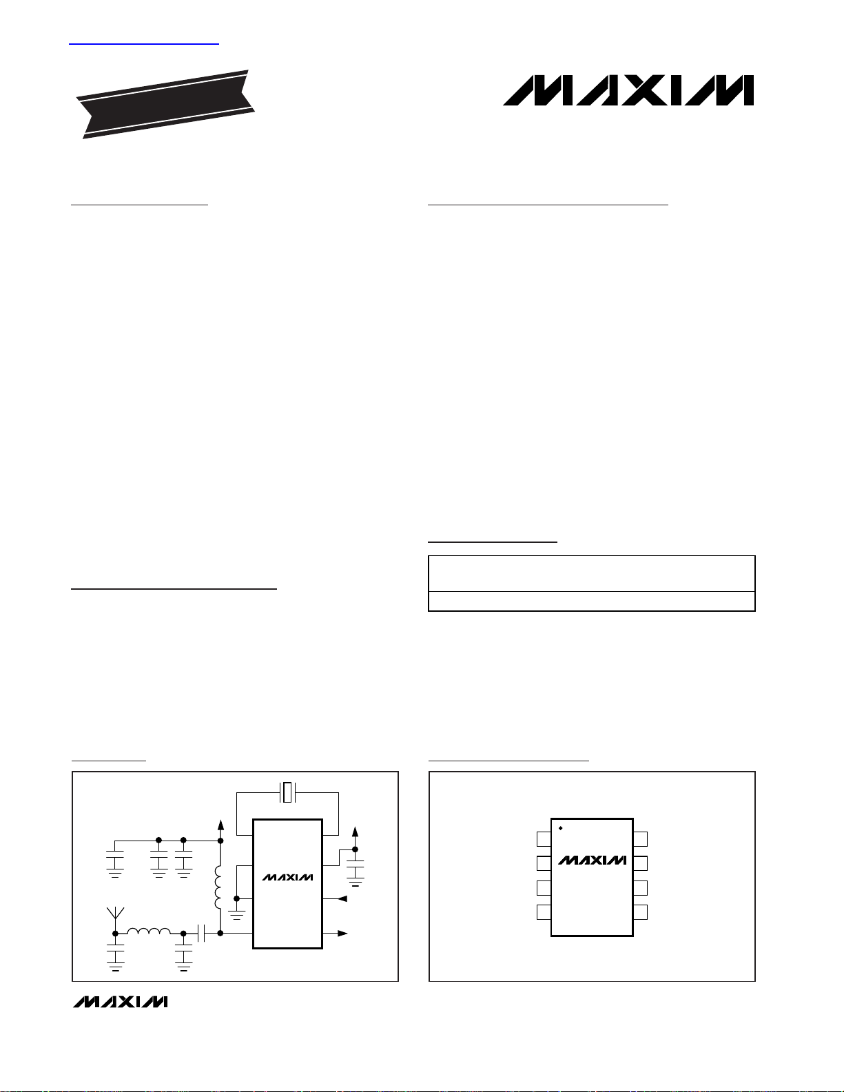
MAX7044
1
XTAL1
ANTENNA
3.0V
3.0V
680pF
220pF
100nF
100nF
XTAL2
f
XTAL
8
2
GND
V
DD
7
3
PAGND
DATA INPUT
CLOCK
OUTPUT
(f
CLKOUT
=
f
XTAL
/16)
DATA
6
4
PAOUT
CLKOUT
5
Typical Application Circuit
19-3221; Rev 0; 1/04
For pricing, delivery, and ordering information, please contact Maxim/Dallas Direct! at
1-888-629-4642, or visit Maxim’s website at www.maxim-ic.com.
EVALUATION KIT
AVAILABLE
PART
TEMP RANGE
PIN-
TOP MARK
MAX7044AKA-T
AEJW
查询MAX7044供应商
PACKAGE
-40°C to +125°C 8 SOT23-8
Page 2
MAX7044
300MHz to 450MHz High-Efficiency,
Crystal-Based +13dBm ASK Transmitter
2 _______________________________________________________________________________________
ABSOLUTE MAXIMUM RATINGS
ELECTRICAL CHARACTERISTICS
(Typical Application Circuit, all RF inputs and outputs are referenced to 50Ω, VDD= +2.1V to +3.6V, TA= -40°C to +125°C, unless
otherwise noted. Typical values are at V
DD
= +2.7V, TA= +25°C, unless otherwise noted.) (Note 1)
Stresses beyond those listed under “Absolute Maximum Ratings” may cause permanent damage to the device. These are stress ratings only, and functional
operation of the device at these or any other conditions beyond those indicated in the operational sections of the specifications is not implied. Exposure to
absolute maximum rating conditions for extended periods may affect device reliability.
VDDto GND ..........................................................-0.3V to +4.0V
All Other Pins to GND ................................-0.3V to (V
DD
+ 0.3V)
Continuous Power Dissipation (T
A
= +70°C)
8-Pin SOT23 (derate 8.9mW/°C above +70°C)............714mW
Operating Temperature Range .........................-40°C to +125°C
Storage Temperature Range .............................-60°C to +150°C
Junction Temperature......................................................+150°C
Lead Temperature (soldering, 10s) .................................+300°C
PARAMETER
SYMBOL
CONDITIONS
MIN
TYP
MAX
UNITS
SYSTEM PERFORMANCE
Supply Voltage V
DD
2.1 3.6 V
V
DATA
at 50% duty
cycle, (Notes 3, 4)
7.7
PA on (Note 5)
fRF = 315MHz
PA off (Note 6) 1.7 2.8
V
DATA
at 50% duty
cycle, (Notes 3, 4)
8.0
PA on (Note 5)
Supply Current
(Note 2)
I
DD
fRF = 433MHz
PA off (Note 6) 1.9 3.1
mA
TA < +25°C 40 130
Standby Current I
STDBY
V
DATA
< VIL for
more than WAIT
time (Notes 4, 7)
T
A
< +125°C
nA
Frequency Range (Note 4) f
RF
450
MHz
Data Rate (Note 4) 0 100
kbps
Modulation Depth (Note 8) ON to OFF P
OUT
ratio 90 dB
TA = +25°C, VDD =
+2.7V
9.6
TA = +125°C, VDD =
+2.1V
5.9 9.0
Output Power, PA On
(Notes 4, 5)
P
OUT
fRF = 300MHz to
450MHz
T
A
= -40°C, VDD =
+3.6V
dBm
Oscillator settled to within 50kHz
Turn-On Time (Note 8) t
ON
Oscillator settled to within 5kHz
µs
fRF = 315MHz 48
Transmit Efficiency with CW
(Notes 5, 10)
f
RF
= 433MHz 47
%
fRF = 315MHz 43
Transmit Efficiency with 50%
OOK (Notes 3, 10)
f
RF
= 433MHz 41
%
14.1
13.8 25.4
14.4
300
13.1 15.8 18.5
14.0 25.7
550 2900
12.5 15.4
12.0
220
450
Page 3
MAX7044
300MHz to 450MHz High-Efficiency,
Crystal-Based +13dBm ASK Transmitter
_______________________________________________________________________________________ 3
ELECTRICAL CHARACTERISTICS (continued)
(Typical Application Circuit, all RF inputs and outputs are referenced to 50Ω, VDD= +2.1V to +3.6V, TA= -40°C to +125°C, unless
otherwise noted. Typical values are at V
DD
= +2.7V, TA= +25°C, unless otherwise noted.) (Note 1)
Note 1: Supply current, output power, and efficiency are greatly dependent on board layout and PAOUT match.
Note 2: Production tested at T
A
= +25°C with fRF= 300MHz and 450MHz. Guaranteed by design and characterization over tem-
perature and frequency.
Note 3: 50% duty cycle at 10kbps with Manchester coding.
Note 4: Guaranteed by design and characterization, not production tested.
Note 5: PA output is turned on in test mode by V
DATA
= VCC/2 + 100mV.
Note 6: PA output is turned off in test mode by V
DATA
= VCC/2 – 100mV.
Note 7: Wait time: t
WAIT
= (216x 32) / fRF.
Note 8: Generally limited by PC board layout.
Note 9: V
DATA
= VILto V
DATA
= VIHafter V
DATA
= VILfor WAIT time: t
WAIT
= (216 x 32) / fRF.
Note 10: V
DATA
= VIH. Efficiency = P
OUT
/(V
DD
x IDD).
PARAMETER
SYMBOL
CONDITIONS
MIN
TYP
MAX
UNITS
PHASE-LOCKED LOOP (PLL)
VCO Gain
MHz/V
f
OFFSET
= 100kHz -80
fRF = 315MHz
f
OFFSET
= 1MHz -90
f
OFFSET
= 100kHz -77
Phase Noise
f
RF
= 433MHz
f
OFFSET
= 1MHz -87
dBc/Hz
fRF = 315MHz -50
Maximum Carrier Harmonics
f
RF
= 433MHz -50
dBc
fRF = 315MHz -74
Reference Spur
f
RF
= 433MHz -80
dBc
Loop Bandwidth 1.6
MHz
Crystal Frequency f
XTAL
MHz
Frequency Pulling by V
DD
3
ppm/V
Maximum Crystal Inductance 50 µH
Crystal Load Capacitance 3pF
DATA INPUT
Data Input High V
IH
V
DD
V
Data Input Low V
IL
V
Maximum Input Current 10 µA
Pulldown Current 10 µA
CLKOUT OUTPUT
Output Voltage Low V
OL
I
SINK
= 650µA (Note 4)
V
Output Voltage High V
OH
I
SOURCE
= 350µA (Note 4)
V
DD
V
Load Capacitance C
LOAD
(Note 4) 10 pF
CLKOUT Frequency
16
Hz
330
fRF/32
0.25
0.25
0.25
0.25
f
XTAL
/
Page 4

MAX7044
300MHz to 450MHz High-Efficiency,
Crystal-Based +13dBm ASK Transmitter
4 _______________________________________________________________________________________
Typical Operating Characteristics
(Typical Application Circuit, VDD= +2.7V, TA= +25°C, unless otherwise noted.) (Note 1)
7
9
11
13
15
17
19
21
23
2.1 2.4 2.7 3.0 3.3 3.6
SUPPLY CURRENT
vs. SUPPLY VOLTAGE
MAX7044 toc01
SUPPLY VOLTAGE (V)
SUPPLY CURRENT (mA)
fRF = 315MHz
PA ON
TA = -40°C
TA = +25°C
TA = +85°C
TA = +125°C
5
6
7
8
9
10
11
12
13
2.1 2.4 2.7 3.0 3.3 3.6
SUPPLY CURRENT
vs. SUPPLY VOLTAGE
MAX7044 toc02
SUPPLY VOLTAGE (V)
SUPPLY CURRENT (mA)
TA = +25°C
fRF = 315MHz
PA 50% DUTY CYCLE AT 10kHz
TA = -40°C
TA = +85°C
TA = +125°C
8
12
10
16
14
20
18
22
2.1 2.72.4 3.0 3.3 3.6
SUPPLY CURRENT
vs. SUPPLY VOLTAGE
MAX7044 toc03
SUPPLY VOLTAGE (V)
SUPPLY CURRENT (mA)
TA = +25°C
fRF = 433MHz
PA ON
TA = -40°C
TA = +85°C
TA = +125°C
6
7
8
9
10
11
12
13
14
2.1 2.4 2.7 3.0 3.3 3.6
SUPPLY CURRENT
vs. SUPPLY VOLTAGE
MAX7044 toc04
SUPPLY VOLTAGE (V)
SUPPLY CURRENT (mA)
TA = +25°C
fRF = 433MHz
PA 50% DUTY CYCLE AT 10kHz
TA = -40°C
TA = +85°C
TA = +125°C
8
10
14
12
16
18
2.1 2.72.4 3.0 3.3 3.6
OUTPUT POWER
vs. SUPPLY VOLTAGE
MAX7044 toc05
SUPPLY VOLTAGE (V)
OUTPUT POWER (dBm)
fRF = 315MHz
PA ON
TA = +25°C
TA = -40°C
TA = +85°C
TA = +125°C
8
10
14
12
16
18
2.1 2.72.4 3.0 3.3 3.6
OUTPUT POWER
vs. SUPPLY VOLTAGE
MAX7044 toc06
SUPPLY VOLTAGE (V)
OUTPUT POWER (dBm)
fRF = 433MHz
PA ON
TA = +25°C
TA = -40°C
TA = +85°C
TA = +125°C
-80
-78
-74
-76
-72
-70
2.1 2.72.4 3.0 3.3 3.6
REFERENCE SPUR MAGNITUDE
vs. SUPPLY VOLTAGE
MAX7044 toc07
SUPPLY VOLTAGE (V)
REFERENCE SPUR MAGNITUDE (dBc)
REFERENCE SPUR = fRF ± f
XTAL
fRF = 433MHz
fRF = 315MHz
-3
-1
-2
1
0
2
3
2.1 2.72.4 3.0 3.3 3.6
FREQUENCY STABILITY
vs. SUPPLY VOLTAGE
MAX7044 toc08
SUPPLY VOLTAGE (V)
FREQUENCY STABILITY (ppm)
fRF = 433MHz
fRF = 315MHz
30
35
40
45
50
55
60
65
70
2.1 2.4 2.7 3.0 3.3 3.6
TRANSMIT POWER EFFICIENCY
vs. SUPPLY VOLTAGE
MAX7044 toc09
SUPPLY VOLTAGE (V)
TRANSMIT POWER EFFICIENCY (%)
fRF = 315MHz
PA ON
TA = -40°C
TA = +85°C
TA = +125°C
TA = +25°C
Page 5

MAX7044
300MHz to 450MHz High-Efficiency,
Crystal-Based +13dBm ASK Transmitter
_______________________________________________________________________________________ 5
20
25
30
35
40
45
50
55
60
2.1 2.4 2.7 3.0 3.3 3.6
TRANSMIT POWER EFFICIENCY
vs. SUPPLY VOLTAGE
MAX7044 toc10
SUPPLY VOLTAGE (V)
TRANSMIT POWER EFFICIENCY (%)
fRF = 315MHz
PA 50% DUTY CYCLE AT 10kHz
TA = -40°C
TA = +85°C
TA = +125°C
TA = +25°C
30
35
40
45
50
55
60
65
70
2.1 2.4 2.7 3.0 3.3 3.6
TRANSMIT POWER EFFICIENCY
vs. SUPPLY VOLTAGE
MAX7044 toc11
SUPPLY VOLTAGE (V)
TRANSMIT POWER EFFICIENCY (%)
fRF = 433MHz
PA ON
TA = -40°C
TA = +85°C
TA = +125°C
TA = +25°C
15
25
20
40
35
30
55
50
45
60
2.1 2.72.4 3.0 3.3 3.6
TRANSMIT POWER EFFICIENCY
vs. SUPPLY VOLTAGE
MAX7044 toc12
SUPPLY VOLTAGE (V)
TRANSMIT POWER EFFICIENCY (%)
fRF = 433MHz
PA 50% DUTY CYCLE AT 10kHz
TA = +25°C
TA = -40°C
TA = +85°C
TA = +125°C
-140
-110
-120
-130
-100
-90
-80
-70
-60
-50
-40
0.01 10.1 10 100 1k 10k
PHASE NOISE vs. OFFSET FREQUENCY
MAX7044 toc13
OFFSET FREQUENCY (Hz)
PHASE NOISE (dBc/Hz)
2
4
6
8
10
12
14
16
18
0110 100 1000 10,000
SUPPLY CURRENT AND OUTPUT POWER
vs. EXTERNAL RESISTOR
MAX7044 toc14
EXTERNAL RESISTOR (Ω)
SUPPLY CURRENT (mA)
-16
-12
-8
-4
0
4
8
12
16
POWER
CURRENT
fRF = 315MHz
PA ON
OUTPUT POWER (dBm)
0
6
3
12
9
15
18
-10 -2 2-6 6 10 14
SUPPLY CURRENT vs. OUTPUT POWER
MAX7044 toc15
OUTPUT POWER (dBm)
SUPPLY CURRENT (mA)
fRF = 315MHz
PA ON
50% DUTY CYCLE
50kHz/div
FREQUENCY SETTLING TIME
MAX7044 toc16
AM DEMODULATION OF PA OUTPUT
DATA RATE = 100kHz
MAX7044 toc17
OUTPUT SPECTRUM
MAX7044 toc18
Typical Operating Characteristics (continued)
(Typical Application Circuit, VDD= +2.7V, TA= +25°C, unless otherwise noted.) (Note 1)
Page 6

Detailed Description
The MAX7044 is a highly integrated ASK transmitter
operating over the 300MHz to 450MHz frequency
band. The IC requires only a few external components
to complete a transmit solution. The MAX7044 includes
a complete PLL and a highly efficient power amplifier.
The device is automatically placed into a low-power
shutdown mode and powers up when data is detected
on the data input.
Shutdown Mode
The MAX7044 has an automatic shutdown mode that
places the device in low-power mode if the DATA input
has not toggled for a specific amount of time (wait time).
The wait time is equal to 2
16
clock cycles of the crystal.
This equates to a wait time of approximately 6.66ms for
MAX7044
300MHz to 450MHz High-Efficiency,
Crystal-Based +13dBm ASK Transmitter
6 _______________________________________________________________________________________
Pin Description
PIN NAME FUNCTION
1 XTAL1 1st Crystal Input. f
XTAL
= fRF / 32.
2 GND Ground. Connect to system ground.
3 PAGND Ground for the Power Amplifier (PA). Connect to system ground.
4 PAOUT
Power-Amplifier Output. The PA output requires a pullup inductor to the supply voltage, which can be
part of the output-matching network to an antenna.
5
Buffered Clock Output. The frequency of CLKOUT is f
XTAL
/ 16.
6 DATA OOK Data Input. DATA also controls the power-up state (see the Shutdown Mode section).
7VDDSupply Voltage. Bypass to GND with a 100nF capacitor as close to the pin as possible.
8 XTAL2 2nd Crystal Input. f
XTAL
= fRF / 32.
Functional Diagram
-55
-52
-46
-49
-43
-40
2.1 2.72.4 3.0 3.3 3.6
CLKOUT SPUR MAGNITUDE
vs. SUPPLY VOLTAGE
MAX7044 toc19
SUPPLY VOLTAGE (V)
CLKOUT SPUR MAGNITUDE (dBc)
fRF = 315MHz
Typical Operating Characteristics (continued)
(Typical Application Circuit, VDD= +2.7V, TA= +25°C, unless otherwise noted.) (Note 1)
CLKOUT
DATA
DATA
ACTIVITY
DETECTOR
XTAL1
XTAL2
LOCK DETECT 32x PLL
CRYSTAL-
OSCILLATOR
DRIVER
MAX7044
PA
/16
V
GND
PAOUT
PAGND
CLKOUT
DD
Page 7

a 315MHz RF frequency and 4.84ms for a 433MHz RF
frequency. For other frequencies, calculate the wait
time with the following equation:
where t
WAIT
is the wait time to shutdown and fRFis the
RF transmit frequency.
When the device is in shutdown, a rising edge on DATA
initiates the warm up of the crystal and PLL. The crystal
and PLL must have 220µs settling time before data can
be transmitted. The 220µs turn-on time of the MAX7044
is dominated by the crystal oscillator startup time. Once
the oscillator is running, the 1.6MHz PLL loop bandwidth allows fast frequency recovery during power
amplifier toggling.
When the device is operating, each edge on the data
line resets an internal counter to zero and it begins to
count again. If no edges are detected on the data line,
the counter reaches the end-of-count (2
16
clock cycles)
and places the device in shutdown mode. If there is an
edge on the data line before the counter hits the end of
count, the counter is reset and the process starts over.
Phase-Locked Loop
The PLL block contains a phase detector, charge
pump, integrated loop filter, VCO, asynchronous 32x
clock divider, and crystal oscillator. This PLL requires
no external components. The relationship between the
carrier and crystal frequency is given by:
f
XTAL
= fRF/ 32
The lock-detect circuit prevents the power amplifier
from transmitting until the PLL is locked. In addition, the
device shuts down the power amplifier if the reference
frequency is lost.
Power Amplifier
The PA of the MAX7044 is a high-efficiency, opendrain, class-C amplifier. With a proper output matching
network, the PA can drive a wide range of impedances,
including the small-loop PC board trace antenna and
any 50Ω antenna. The output-matching network for an
antenna with a characteristic impedance of 50Ω is
shown in the Typical Application Circuit. The output-
matching network suppresses the carrier harmonics
and transforms the antenna impedance to an optimal
impedance at PAOUT, which is about 125Ω.
When the output matching network is properly tuned,
the power amplifier transmits power with high efficiency.
The Typical Application Circuit delivers +13dBm at
+2.7V supply with 7.7mA of supply current. Thus, the
overall efficiency is 48% with the efficiency of the power
amplifier itself greater than 54%.
Buffered Clock Output
The MAX7044 provides a buffered clock output
(CLKOUT) for easy interface to a microcontroller or frequency-hopping generator. The frequency of CLKOUT is
1/16 the crystal frequency. For a 315MHz RF transmit frequency, a crystal of 9.84375MHz is used, giving a clock
output of 615.2kHz. For a 433.92MHz RF frequency, a
crystal of 13.56MHz is used for a clock output of
847.5kHz.
The clock output is inactive when the device is in shut-
down mode. The device is placed in shutdown mode by
the internal data activity detector (see the Shutdown
Mode section). Once data is detected on the data input,
the clock output is stable after approximately 220µs.
Applications Information
Output Power Adjustment
It is possible to adjust the output power down to -15dBm
with the addition of a resistor (see R
PWRADJ
in Figure 1).
The addition of the power adjust resistor also reduces
power consumption. See the Supply Current and
Output Power vs. External Resistor and Supply Current
vs. Output Power graphs in the Typical Operating
Characteristics section. It is imperative to add both a
low-frequency and a high-frequency decoupling
capacitor as shown in Figure 1.
Crystal Oscillator
The crystal oscillator in the MAX7044 is designed to
present a capacitance of approximately 3pF between
the XTAL1 and XTAL2 pins. If a crystal designed to
oscillate with a different load capacitance is used, the
crystal is pulled away from its intended operating fre-
t
x
f
WAIT
RF
=
232
16
MAX7044
300MHz to 450MHz High-Efficiency,
Crystal-Based +13dBm ASK Transmitter
_______________________________________________________________________________________ 7
MAX1434
1
XTAL1
ANTENNA
3.0V
3.0V
680pF
R
PWRADJ
220pF
100nF
100nF
XTAL2
f
XTAL
8
2
GND
V
DD
7
3
PAGND
DATA INPUT
CLOCK
OUTPUT
(f
CLKOUT
=
f
XTAL
/16)
DATA
6
4
PAOUT
CLKOUT
5
Figure 1. Output Power Adjustment Circuit
Page 8

MAX7044
quency, thus introducing an error in the reference frequency. Crystals designed to operate with higher differential load capacitance always pull the reference
frequency higher. For example, a 9.84375MHz crystal
designed to operate with a 10pF load capacitance
oscillates at 9.84688MHz with the MAX7044, causing
the transmitter to be transmitting at 315.1MHz rather
than 315.0MHz, an error of about 100kHz, or 320ppm.
In actuality, the oscillator pulls every crystal. The crystal’s natural frequency is really below its specified frequency, but when loaded with the specified load
capacitance, the crystal is pulled and oscillates at its
specified frequency. This pulling is already accounted
for in the specification of the load capacitance.
Additional pulling can be calculated if the electrical
parameters of the crystal are known. The frequency
pulling is given by:
where:
f
p
is the amount the crystal frequency is pulled in ppm.
Cmis the motional capacitance of the crystal.
C
case
is the case capacitance.
C
spec
is the specified load capacitance.
C
load
is the actual load capacitance.
When the crystal is loaded as specified, i.e., C
load
=
C
spec
, the frequency pulling equals zero.
Output Matching to 50Ω
When matched to a 50Ω system, the MAX7044 PA is
capable of delivering up to +13dBm of output power at
VDD= 2.7V. The output of the PA is an open-drain transistor that requires external impedance matching and
pullup inductance for proper biasing. The pullup inductance from PA to VDDserves three main purposes: it
resonates the capacitance of the PA output, provides
biasing for the PA, and becomes a high-frequency
choke to reduce the RF energy coupling into VDD. The
recommended output-matching network topology is
shown in the Typical Application Circuit. The matching
network transforms the 50Ω load to approximately
125Ω at the output of the PA in addition to forming a
bandpass filter that provides attenuation for the higher
order harmonics.
Output Matching to
PC Board Loop Antenna
In some applications, the MAX7044 power amplifier
output has to be impedance matched to a small-loop
antenna. The antenna is usually fabricated out of a copper trace on a PC board in a rectangular, circular, or
square pattern. The antenna will have an impedance
that consists of a lossy component and a radiative
component. To achieve high radiating efficiency, the
radiative component should be as high as possible,
while minimizing the lossy component. In addition, the
loop antenna will have an inherent loop inductance
associated with it (assuming the antenna is terminated
to ground). For example, in a typical application, the
radiative impedance is less than 0.5Ω, the lossy imped-
ance is less than 0.7Ω, and the inductance is approximately 50nH to 100nH.
The objective of the matching network is to match the
power amplifier output to the small-loop antenna. The
matching components thus transform the low radiative
and resistive parts of the antenna into the much higher
value of the PA output. This gives higher efficiency. The
low radiative and lossy components of the small-loop
antenna result in a higher Q matching network than the
50Ω network; thus, the harmonics are lower.
Layout Considerations
A properly designed PC board is an essential part of
any RF/microwave circuit. At the power amplifier output, use controlled-impedance lines and keep them as
short as possible to minimize losses and radiation. At
high frequencies, trace lengths that are approximately
1/20 the wavelength or longer become antennas. For
example, a 2in trace at 315MHz can act as an antenna.
Keeping the traces short also reduces parasitic inductance. Generally, 1in of PC board trace adds about
20nH of parasitic inductance. The parasitic inductance
can have a dramatic effect on the effective inductance.
For example, a 0.5in trace connecting a 100nH inductor adds an extra 10nH of inductance, or 10%.
To reduce the parasitic inductance, use wider traces
and a solid ground or power plane below the signal
traces. Using a solid ground plane can reduce the parasitic inductance from approximately 20nH/in to 7nH/in.
Also, use low-inductance connections to ground on all
GND pins, and place decoupling capacitors close to all
V
DD
connections.
Chip Information
TRANSISTOR COUNT: 2489
PROCESS: CMOS
f
C
C
case
CCC
x
p
m
load case spec
=
+
−
+
2
11
10
6
300MHz to 450MHz High-Efficiency,
Crystal-Based +13dBm ASK Transmitter
8 _______________________________________________________________________________________
Page 9

MAX7044
300MHz to 450MHz High-Efficiency,
Crystal-Based +13dBm ASK Transmitter
Maxim cannot assume responsibility for use of any circuitry other than circuitry entirely embodied in a Maxim product. No circuit patent licenses are
implied. Maxim reserves the right to change the circuitry and specifications without notice at any time.
Maxim Integrated Products, 120 San Gabriel Drive, Sunnyvale, CA 94086 408-737-7600 _____________________ 9
© 2004 Maxim Integrated Products Printed USA is a registered trademark of Maxim Integrated Products.
Package Information
(The package drawing(s) in this data sheet may not reflect the most current specifications. For the latest package outline information,
go to www.maxim-ic.com/packages
).
SOT23, 8L .EPS
REV.DOCUMENT CONTROL NO.APPROVAL
PROPRIETARY INFORMATION
TITLE:
3.002.60E
C
E1
E
BETWEEN 0.08mm AND 0.15mm FROM LEAD TIP.
8. MEETS JEDEC MO178.
8∞
0.60
1.75
0.30
L2
0∞
e1
e
L
1.50E1
0.65 BSC.
1.95 REF.
0.25 BSC.
GAUGE PLANE
SEATING PLANE C
C
L
PIN 1
I.D. DOT
(SEE NOTE 6)
L
C
L
C
A2
e1
D
DETAIL "A"
5. COPLANARITY 4 MILS. MAX.
NOTE:
7. SOLDER THICKNESS MEASURED AT FLAT SECTION OF LEAD
6. PIN 1 I.D. DOT IS 0.3 MM ÿ MIN. LOCATED ABOVE PIN 1.
4. PACKAGE OUTLINE INCLUSIVE OF SOLDER PLATING.
3. PACKAGE OUTLINE EXCLUSIVE OF MOLD FLASH & METAL BURR.
HEEL OF THE LEAD PARALLEL TO SEATING PLANE C.
2. FOOT LENGTH MEASURED FROM LEAD TIP TO UPPER RADIUS OF
1. ALL DIMENSIONS ARE IN MILLIMETERS.
L2
L
A1
A
0.45
1.30
0.15
1.45
MAX
0.28b
0.90A2
0.00A1
0.90
A
MIN
SYMBOL
3.00
0.20
2.80D
0.09
C
SEE DETAIL "A"
L
C
b
e
D
1
21-0078
1
PACKAGE OUTLINE, SOT-23, 8L BODY
0
0
 Loading...