MAXIM MAX7036 Technical data

General Description
The MAX7036 low-cost receiver is designed to receive
amplitude-shift-keyed (ASK) and on-off-keyed (OOK)
data in the 300MHz to 450MHz frequency range. The
receiver has an RF input signal range of -109dBm to
0dBm.
The MAX7036 requires few external components and
has a power-down pin to put it in a low-current sleep
mode, making it ideal for cost- and power-sensitive
applications. The low-noise amplifier (LNA), phaselocked loop (PLL), mixer, IF filter, received-signalstrength indicator (RSSI), and baseband sections are
all on-chip. The MAX7036 uses a very-low intermediate
frequency (VLIF) architecture. The MAX7036 integrates
the IF filter on-chip and therefore eliminates an external
ceramic filter, reducing the bill-of-materials cost. The
device also contains an on-chip automatic gain control
(AGC) that reduces the LNA gain by 30dB when the
input signal power is large. The MAX7036 operates
from either a 5V or a 3.3V power supply and draws
5.5mA (typ) of current.
The MAX7036 is available in a 20-pin thin QFN package with an exposed pad and is specified over the
AEC-Q100 Level 2 (-40°C to +105°C) temperature
range.
Applications
Low-Cost RKE
Garage Door Openers
Remote Controls
Home Automation
Sensor Networks
Security Systems
Features
o ASK/OOK Modulation
o < 250µs Enable Turn-On Time
o On-Chip PLL, VCO, Mixer, IF, Baseband
o Low IF (200kHz Nominal)
o 5.5mA DC Current
o 1µA Standby Current
o 3.3V/5V Operation
o Small 20-Pin Thin QFN Package with an Exposed
Pad
MAX7036
300MHz to 450MHz ASK Receiver
with Internal IF Filter
________________________________________________________________
Maxim Integrated Products
1
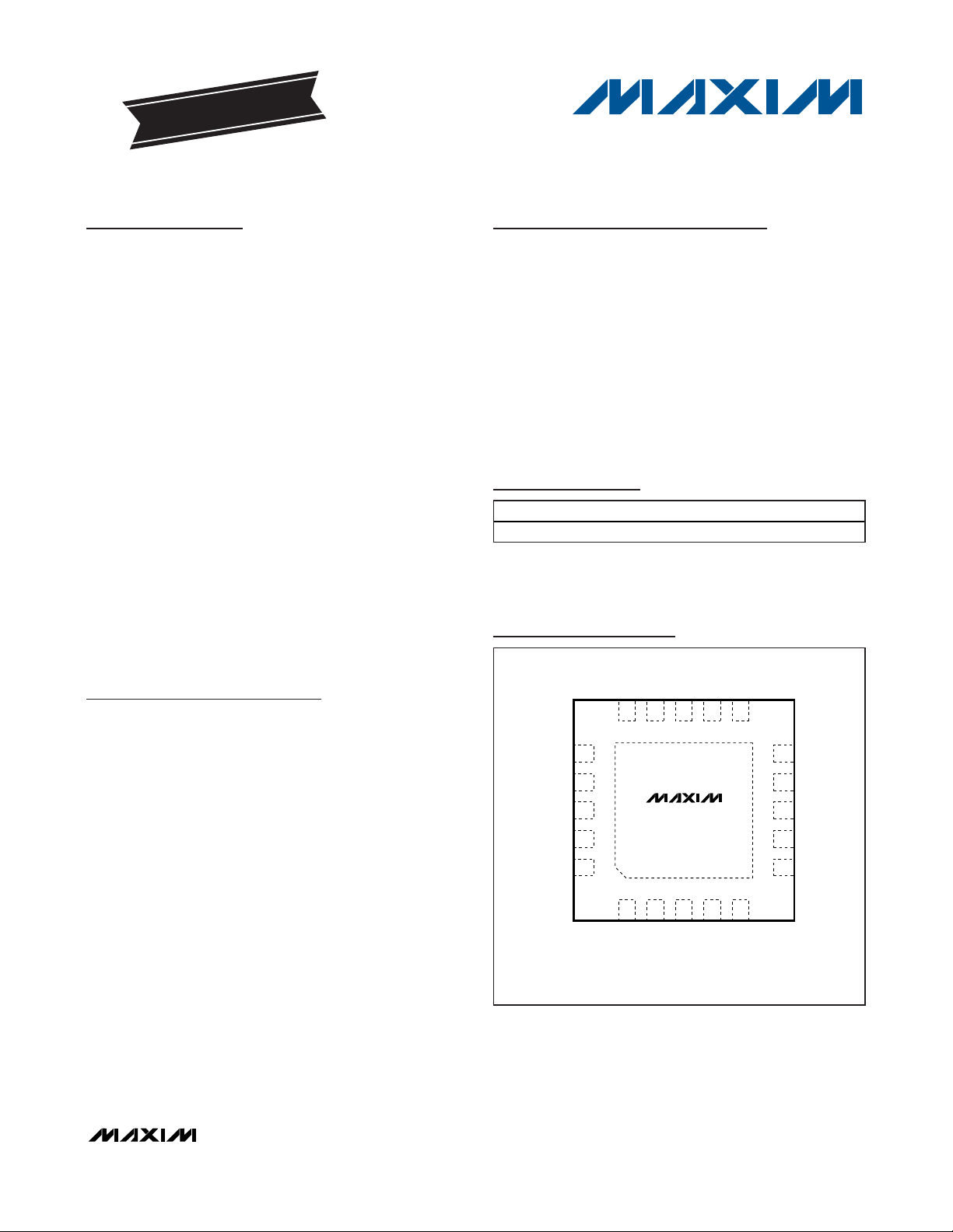
Pin Configuration
Ordering Information
19-4386; Rev 1; 8/10
For pricing, delivery, and ordering information, please contact Maxim Direct at 1-888-629-4642,
or visit Maxim’s website at www.maxim-ic.com.
EVALUATION KIT
AVAILABLE
PART TEMP RANGE PIN-PACKAGE
-40°C to +105°C
20 Thin QFN-EP*
/V
denotes an automotive qualified part.
+
Denotes a lead(Pb)-free/RoHS-compliant package.
*
EP = Exposed pad.
MAX7036GTP/V+
TOP VIEW
DSP
DSN
PDOUT
V
DATAOUT
OPP
DFFB
15 14 12 11
16
17
18
19
DD
20
+
MAX7036
13
DCOC
DVDD
IFC3
IFC1
10
IFC2
9
8
MIXIN1
MIXIN2
7
LNAOUT
6
EP
12
XTAL2
ENABLE
THIN QFN
5mm x 5mm
45
3
AVDD
XTAL1
LNAIN

MAX7036
300MHz to 450MHz ASK Receiver
with Internal IF Filter
2 _______________________________________________________________________________________
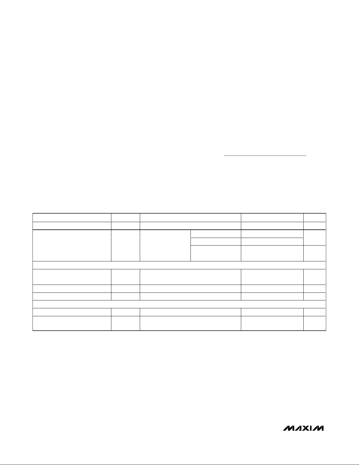
ABSOLUTE MAXIMUM RATINGS
3.3V DC ELECTRICAL CHARACTERISTICS
(
Typical Application Circuit
, 50Ω system impedance, V
AVDD
= V
DVDD
= VDD= 3.0V to 3.6V, fRF= 300MHz to 450MHz, TA= -40°C to
+105°C, unless otherwise noted. Typical values are at V
AVDD
= V
DVDD
= VDD= 3.3V, TA= +25°C, unless otherwise noted.) (100%
tested at T
A
= +105°C.)
Stresses beyond those listed under “Absolute Maximum Ratings” may cause permanent damage to the device. These are stress ratings only, and functional
operation of the device at these or any other conditions beyond those indicated in the operational sections of the specifications is not implied. Exposure to
absolute maximum rating conditions for extended periods may affect device reliability.
VDDto GND...........................................................-0.3V to +6.0V
AVDD to GND........................................................-0.3V to +4.0V
DVDD to GND........................................................-0.3V to +4.0V
ENABLE to GND.........................................-0.3V to (V
DD
+ 0.3V)
LNAIN to GND .......................................................-0.3V to +1.2V
All Other Pins to GND.............................-0.3V to (V
DVDD
+ 0.3V)
Continuous Power Dissipation (T
A
= +70°C)
20-Pin TQFN (derate 20.8mW/°C above +70°C) ....1666.7mW
Junction-to-Case Thermal Resistance (θ
JC
) (Note 1)
20-Pin TQFN...................................................................2°C/W
Junction-to-Ambient Thermal Resistance (θ
JA
) (Note 1)
20-Pin TQFN.................................................................48°C/W
Operating Temperature Range .........................-40°C to +105°C
Junction Temperature......................................................+150°C
Storage Temperature Range .............................-65°C to +150°C
Lead Temperature (soldering, 10s) .................................+300°C
Soldering Temperature (reflow) .......................................+260°C
Note 1: Package thermal resistances were obtained using the method described in JEDEC specification JESD51-7, using a single-
layer board. For detailed information on package thermal considerations, go to www.maxim-ic.com/thermal-tutorial
.
Supply Voltage V
Supply Current I
DIGITAL INPUT (ENABLE)
Input High Voltage V
Input Low Voltage V
Input Current I
DIGITAL OUTPUT (DATAOUT)
Output Low Voltage V
Output High Voltage V
PARAMETER SYMBOL CONDITIONS MIN TYP MAX UNITS
IH
IL
V
AVDD
TA < +105°C
V
AVDD
V
AVDD
0 ≤ V
I
SINK
I
SOURCE
DD
IN
ENABLE
OL
OH
= V
DVDD
= V
DVDD
= V
DVDD
ENABLE
= 100μA 0.4 V
= 100μA
≤ V
= V
DD
fRF = 315MHz 5.3 6.7
fRF = 433MHz 5.8 7.3
Deep-sleep mode,
ENABLE
= 0V
= V
= V
DD
V
DD
DD
3.0 3.3 3.6 V
VDD -
0.4
V
-
DD
0.4
1 2.7 μA
0.4 V
20 μA
mA
V
V

MAX7036
300MHz to 450MHz ASK Receiver
with Internal IF Filter
_______________________________________________________________________________________ 3
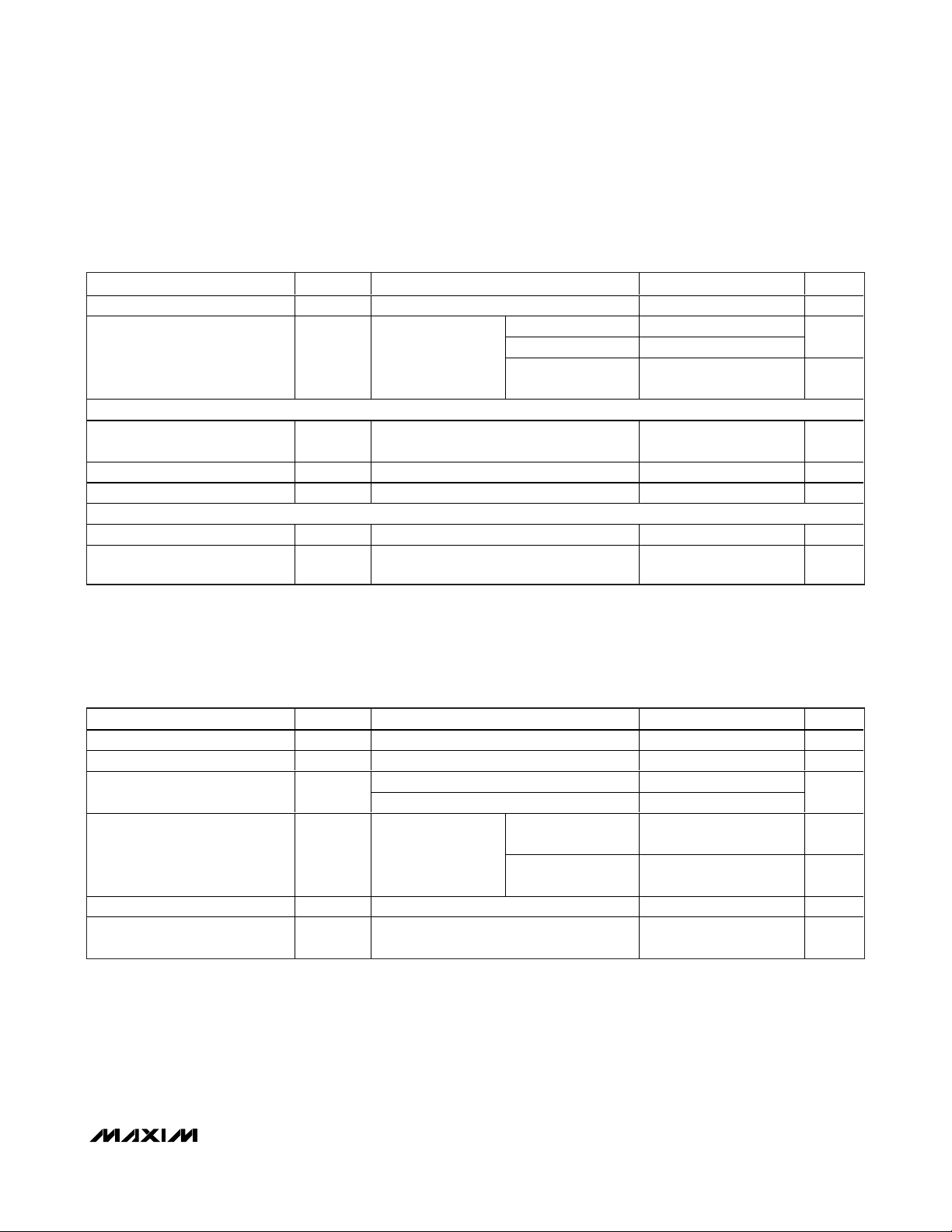
5.0V DC ELECTRICAL CHARACTERISTICS
(
Typical Application Circuit
, 50Ω system impedance, VDD= 4.5V to 5.5V, fRF= 300MHz to 450MHz, TA= -40°C to +105°C, unless
otherwise noted. Typical values are at V
DD
= 5.0V, TA= +25°C, unless otherwise noted.) (100% tested at TA= +105°C.)
AC ELECTRICAL CHARACTERISTICS
(
Typical Application Circuit
, 50Ω system impedance, V
AVDD
= V
DVDD
= VDD= 3.0V to 3.6V, fRF= 300MHz to 450MHz, TA= -40°C to
+105°C, unless otherwise noted. Typical values are at V
AVDD
= V
DVDD
= VDD= 3.3V, TA= +25°C, fRF= 315MHz, unless otherwise
noted.) (100% tested at T
A
= +105°C.)
PARAMETER SYMBOL CONDITIONS MIN TYP MAX UNITS
Supply Voltage V
Supply Current I
DIGITAL INPUT (ENABLE)
Input High Voltage V
Input Low Voltage V
Input Current I
DIGITAL OUTPUT (DATAOUT)
Output Low Voltage V
Output High Voltage V
DD
IH
IL
TA < +105°C
V
= V
AVDD
V
AVDD
0 ≤ V
I
SINK
I
SOURCE
DVDD
= V
DVDD
ENABLE
= 100μA 0.4 V
= 100μA
IN
ENABLE
OL
OH
≤ V
4.5 5.0 5.5 V
fRF = 315MHz 5.4 6.8
fRF = 433MHz 5.9 7.4
Deep-sleep mode,
ENABLE
= 0V
VDD -
0.4
V
DD
0.4
-
V
DD
mA
1 3.4 μA
V
0.4 V
20 μA
V
PARAMETER SYMBOL CONDITIONS MIN TYP MAX UNITS
Receiver Input Frequency Range f
Maximum Receiver Input Level P
Sensitivity (Note 2)
Power-On Time t
AGC Hysteresis 5dB
AGC Low Gain-to-High Gain
Switching Time
RF
RFIN
ON
fRF = 315MHz -109
= 433MHz -107
f
RF
Time for valid RSSI
output, does not
include baseband
filter settling
300 450 MHz
0 dBm
Enable power on
(V
> 3.0V)
DD
V
power on 1 ms
DD
250 μs
13 ms
dBm

MAX7036
300MHz to 450MHz ASK Receiver
with Internal IF Filter
4 _______________________________________________________________________________________
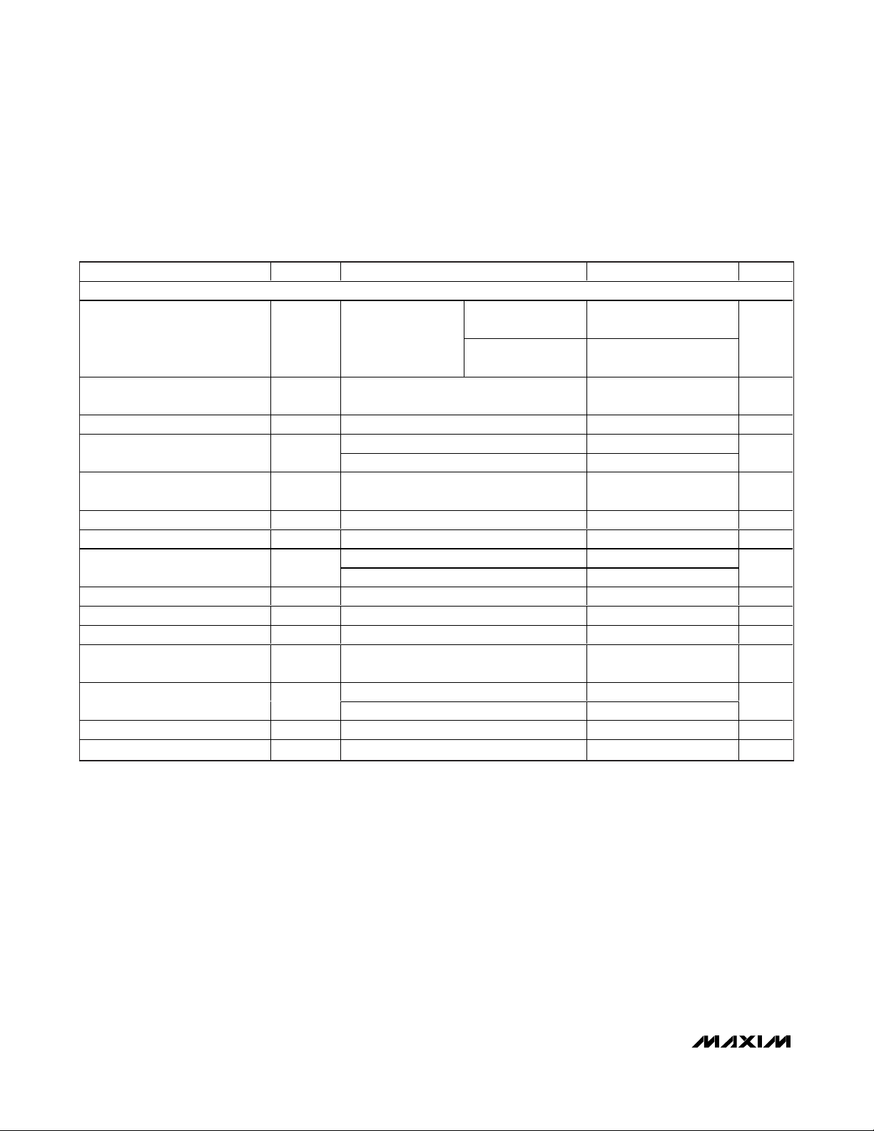
AC ELECTRICAL CHARACTERISTICS (continued)
(
Typical Application Circuit
, 50Ω system impedance, V
AVDD
= V
DVDD
= VDD= 3.0V to 3.6V, fRF= 300MHz to 450MHz, TA= -40°C to
+105°C, unless otherwise noted. Typical values are at V
AVDD
= V
DVDD
= VDD= 3.3V, TA= +25°C, fRF= 315MHz, unless otherwise
noted.) (100% tested at T
A
= +105°C.)
Note 2: BER = 2 x 10⁻³, Manchester coded, data rate = 4kbps. IF bandwidth = 400kHz.
LNA/MIXER
LNA Input Impedance Z
LO Signal Feedthrough to
Antenna
Voltage Gain Reduction Low-gain mode, AGC enabled 29 dB
LNA/Mixer Voltage Gain
3dB Cutoff Frequency BW
RSSI Linearity ±0.5 dB
RSSI Dynamic Range Includes AGC 80 dB
RSSI Level
Intermediate Frequency f
Maximum Data-Filter Bandwidth BW
Maximum Data-Slicer Bandwidth BW
Maximum Peak Detector
Bandwidth
Maximum Data Rate
Crystal Frequency f
Crystal Load Capacitance C
PARAMETER SYMBOL CONDITIONS MIN TYP MAX UNITS
INLNA
IF
IF
DF
DS
XTAL
LOAD
Normalized to 50Ω
High-gain LNA mode 55
Low-gain LNA mode 26
Set by capacitors on IFC1 and IFC2 (see
the Typical Application Circuit)
P
< -120dBm 1.34
RFIN
P
> 0dBm, AGC enabled 2.35
RFIN
Manchester coded 33
Nonreturn to zero (NRZ) 66
fRF = 315MHz
= 433MHz
f
RF
9.36 14.06 MHz
0.4 j5.6
0.4 j4.0
-75 dBm
400 kHz
200 kHz
50 kHz
100 kHz
50 kHz
10 pF
Ω
dB
V
kbps
 Loading...