

Page 1
General Description
The MAX7031 crystal-based, fractional-N transceiver is
designed to transmit and receive FSK data at factorypreset carrier frequencies of 308MHz†, 315MHz, or
433.92MHz with data rates up to 33kbps (Manchester
encoded) or 66kbps (NRZ encoded). This device generates a typical output power of +10dBm into a 50Ω
load, and exhibits typical sensitivity of -110dBm. The
MAX7031 features separate transmit and receive pins
(PAOUT and LNAIN) and provides an internal RF switch
that can be used to connect the transmit and receive
pins to a common antenna.
The MAX7031 transmit frequency is generated by a 16bit, fractional-N, phase-locked loop (PLL), while the
receiver’s local oscillator (LO) is generated by an integer-N PLL. This hybrid architecture eliminates the need
for separate transmit and receive crystal reference
oscillators because the fractional-N PLL is preset to be
10.7MHz above the receive LO. Retaining the fixed-N
PLL for the receiver avoids the higher current-drain
requirements of a fractional-N PLL and keeps the
receiver current drain as low as possible.
The fractional-N architecture of the MAX7031 transmit
PLL allows the transmit FSK signal to be preset for
exact frequency deviations, and completely eliminates
the problems associated with oscillator-pulling FSK signal generation. All frequency-generation components
are integrated on-chip, and only a crystal, a 10.7MHz IF
filter, and a few discrete components are required to
implement a complete antenna/digital data solution.
The MAX7031 is available in a small, 5mm x 5mm, 32pin, thin QFN package, and is specified to operate in
the automotive -40°C to +125°C temperature range.
†
Consult factory for availability.
Applications
2-Way Remote Keyless Entry
Security Systems
Home Automation
Remote Controls
Remote Sensing
Smoke Alarms
Garage-Door Openers
Local Telemetry Systems
Features
o +2.1V to +3.6V or +4.5V to +5.5V Single-Supply
Operation
o Single-Crystal Transceiver
o Factory-Preset Frequency (No Serial Interface
Required)
o FSK Modulation
o Factory-Preset FSK Frequency Deviation
o +10dBm Output Power into 50Ω Load
o Integrated TX/RX Switch
o Integrated Transmit and Receive PLL, VCO, and
Loop Filter
o > 45dB Image Rejection
o Typical RF Sensitivity*: -110dBm
o Selectable IF Bandwidth with External Filter
o RSSI Output with High Dynamic Range
o < 12.5mA Transmit-Mode Current
o < 6.7mA Receive-Mode Current
o < 800nA Shutdown Current
o Fast-On Startup Feature, < 250µs
o Small, 32-Pin, Thin QFN Package
MAX7031
Low-Cost, 308MHz, 315MHz, and 433.92MHz
FSK Transceiver with Fractional-N PLL
________________________________________________________________
Maxim Integrated Products
1
Ordering Information
19-3707; Rev 3; 11/10
For pricing, delivery, and ordering information, please contact Maxim Direct at 1-888-629-4642,
or visit Maxim’s website at www.maxim-ic.com.
*
0.2% BER, 4kbps Manchester-encoded data, 280kHz IF BW
+
Denotes a lead(Pb)-free/RoHs-compliant package.
**
EP = Exposed pad.
Note: The MAX7031 is available with factory-preset operating
frequencies. See the Selector Guide for complete part numbers.
Pin Configuration, Selector Guide, Typical Application
Circuit, and Functional Diagram appear at end of data sheet.
PART TEMP RANGE PIN-PACKAGE
MAX7031_ATJ__+ -40°C to +125°C 32 Thin QFN-EP**
Page 2
MAX7031
Low-Cost, 308MHz, 315MHz, and 433.92MHz
FSK Transceiver with Fractional-N PLL
2 _______________________________________________________________________________________
ABSOLUTE MAXIMUM RATINGS
Stresses beyond those listed under “Absolute Maximum Ratings” may cause permanent damage to the device. These are stress ratings only, and functional
operation of the device at these or any other conditions beyond those indicated in the operational sections of the specifications is not implied. Exposure to
absolute maximum rating conditions for extended periods may affect device reliability.
HVIN to GND .........................................................-0.3V to +6.0V
PAVDD, AVDD, DVDD to GND..............................-0.3V to +4.0V
ENABLE, T/R, DATA, AGC0, AGC1,
AUTOCAL to GND ...............................-0.3V to (V
HVIN
+ 0.3)V
All Other Pins to GND .............................-0.3V to (V
_VDD
+ 0.3)V
Continuous Power Dissipation (T
A
= +70°C)
32-Pin Thin QFN (derate 21.3mW/°C
above +70°C).............................................................1702mW
Operating Temperature Range .........................-40°C to +125°C
Storage Temperature Range .............................-65°C to +150°C
Lead Temperature (soldering, 10s) .................................+300°C
Soldering Temperature (reflow) .......................................+260°C
DC ELECTRICAL CHARACTERISTICS
(
Typical Application Circuit
, 50Ω system impedance, V
PAV
DD
= V
AV
DD
= V
DV
DD
= V
HV
IN
= +2.1V to +3.6V, fRF= 308MHz, 315MHz, or
433.92MHz, T
A
= -40°C to +125°C, unless otherwise noted. Typical values are at V
PAV
DD
= V
AV
DD
= V
DV
DD
= V
HV
IN
= +2.7V,
T
A
= +25°C, unless otherwise noted.) (Note 1)
PARAMETER SYMBOL CONDITIONS MIN TYP MAX UNITS
Supply Voltage (3V Mode) V
Supply Voltage (5V Mode) V
Supply Current I
Voltage Regulator V
DIGITAL I/O
Input-High Threshold V
Input-Low Threshold V
Pulldown Sink Current
Output Low Voltage V
Output High Voltage V
DD
HVIN
HVIN, PAVDD, AVDD, and DVDD
connected to power supply
PAVDD, AVDD, and DVDD unconnected
from HVIN, but connected together
Transmit mode
(Note 2)
TA < +85°C,
typ at +25°C
DD
(Note 3)
TA < +125°C,
typ at +125°C
(Note 2)
REG
V
HVIN
(Note 2)
IH
(Note 2)
IL
AGC0-1, AUTOCAL, ENABLE, T/R, DATA
(V
OL
OH
I
SINK
I
SOURCE
fRF = 315MHz 11.6 19.1
f
= 434MHz 12.4 20.4
RF
Receiver 315MHz 6.4 8.4
Receiver 434MHz 6.7 8.7
Deep-sleep (3V mode) 0.8 8.8
Deep-sleep (5V mode) 2.4 10.9
Receiver 315MHz 6.8 8.7
Receiver 434MHz 7.0 8.8
Deep-sleep (3V mode) 8.0 34.2
Deep-sleep (5V mode) 14.9 39.3
HVIN
= 5V, I
= 5.5V)
= 15mA 3.0 V
LOAD
= 500µA 0.15 V
= 500µA
2.1 2.7 3.6 V
4.5 5.0 5.5 V
0.9 x
V
HVIN
0.1 x
V
HVIN
20 µA
V
HVIN
- 0.26
mA
µA
mA
µA
V
V
V
Page 3
MAX7031
Low-Cost, 308MHz, 315MHz, and 433.92MHz
FSK Transceiver with Fractional-N PLL
_______________________________________________________________________________________ 3
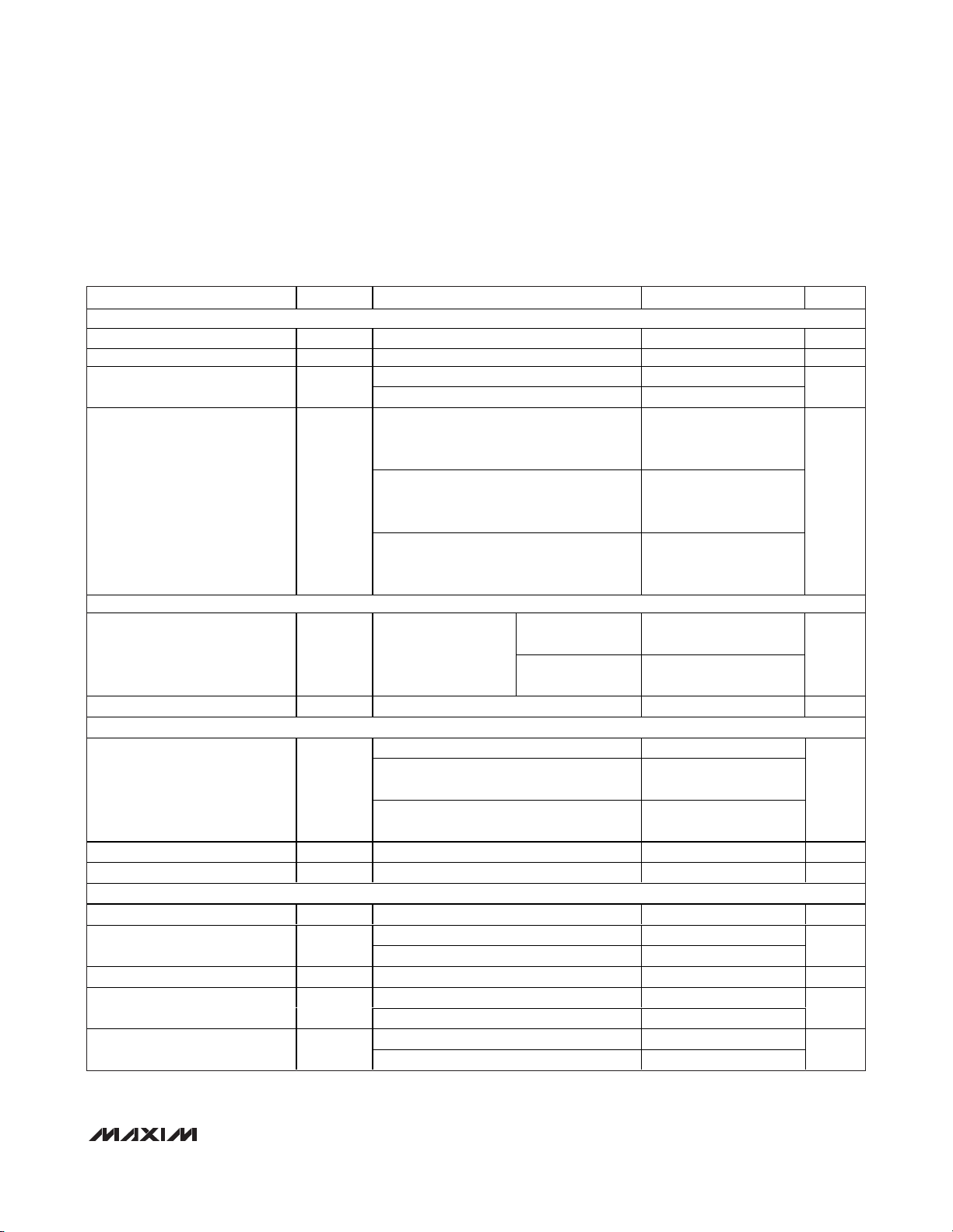
AC ELECTRICAL CHARACTERISTICS
(
Typical Application Circuit
, 50Ω system impedance, V
PAV
DD
= V
AV
DD
= V
DV
DD
= V
HV
IN
= +2.1V to +3.6V, fRF= 308MHz, 315MHz. or
433.92MHz, T
A
= -40°C to +125°C, unless otherwise noted. Typical values are at V
PAV
DD
= V
AV
DD
= V
DV
DD
= V
HV
IN
= +2.7V,
T
A
= +25°C, unless otherwise noted.) (Note 1)
GENERAL CHARACTERISTICS
Frequency Range 308/315/433.92 MHz
Maximum Input Level P
Transmit Efficiency (Note 5)
Power-On Time t
RECEIVER
Sensitivity
Image Rejection 46 dB
POWER AMPLIFIER
Output Power P
Maximum Carrier Harmonics With output matching network -40 dBc
Reference Spur -50 dBc
PHASE-LOCKED LOOP
Transmit VCO Gain K
Transmit PLL Phase Noise
Receive VCO Gain 340 MHz/V
Receive PLL Phase Noise
Loop Bandwidth
PARAMETER SYMBOL CONDITIONS MIN TYP MAX UNITS
RFIN
fRF = 315MHz 32
f
RF
ENABLE or T/R transition low to high,
transmitter frequency settled to within
50kHz of the desired carrier
ENABLE or T/R transition low to high,
ON
OUT
VCO
transmitter frequency settled to within 5kHz
of the desired carrier
ENABLE transition low to high, or T/R
transition high to low, receiver startup time
(Note 4)
0.2% BER, 4kbps
Manchester data rate,
280kHz IF BW, FSK
±50kHz deviation
TA = +25°C (Note 3) 4.6 10.0 15.5
TA = +125°C, V
V
TA = -40°C, V
V
10kHz offset, 200kHz loop BW -68
1MHz offset, 200kHz loop BW -98
10kHz offset, 500kHz loop BW -80
1MHz offset, 500kHz loop BW -90
Transmit PLL 200
Receive PLL 500
= 434MHz 30
= +2.1V (Note 2)
HVIN
= +3.6V (Note 3)
HVIN
PAVDD
PAVDD
= V
315MHz -110
434MHz -107
= V
AVDD
= V
AVDD
= V
DVDD
DVDD
=
=
3.9 6.7
0 dBm
200
350
250
13.1 15.8
340 MHz/V
dBc/Hz
dBc/Hz
%
µs
dBm
dBm
kHz
Page 4
MAX7031
Low-Cost, 308MHz, 315MHz, and 433.92MHz
FSK Transceiver with Fractional-N PLL
4 _______________________________________________________________________________________
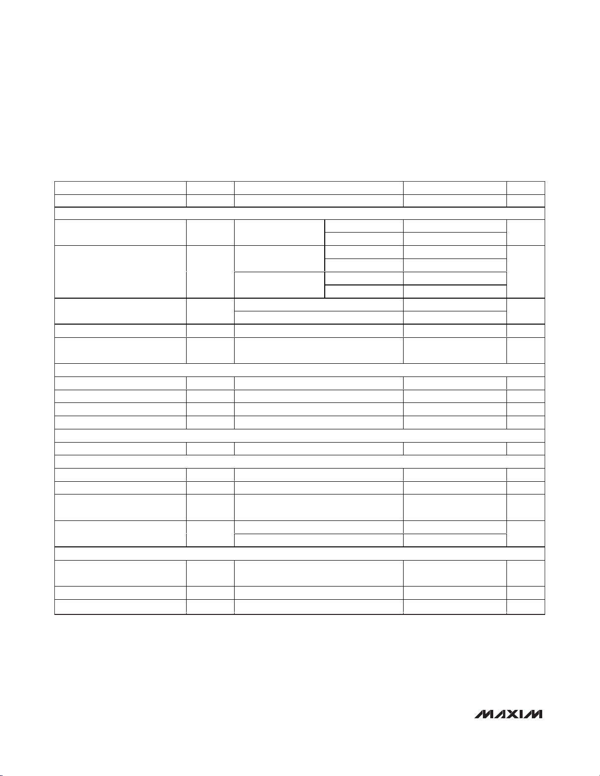
AC ELECTRICAL CHARACTERISTICS (continued)
(
Typical Application Circuit
, 50Ω system impedance, V
PAV
DD
= V
AV
DD
= V
DV
DD
= V
HV
IN
= +2.1V to +3.6V, fRF= 308MHz, 315MHz. or
433.92MHz, T
A
= -40°C to +125°C, unless otherwise noted. Typical values are at V
PAV
DD
= V
AV
DD
= V
DV
DD
= V
HV
IN
= +2.7V,
T
A
= +25°C, unless otherwise noted.) (Note 1)
Reference Frequency Input Level 0.5 V
LOW-NOISE AMPLIFIER/MIXER (Note 7)
LNA Input Impedance Z
Voltage-Conversion Gain
Input-Referred 3rd-Order
Intercept Point
Mixer Output Impedance 330 Ω
LO Signal Feedthrough to
Antenna
RSSI
Input Impedance 330 Ω
Operating Frequency f
3dB Bandwidth 10 MHz
Gain 15 mV/dB
FSK DEMODULATOR
Conversion Gain 2.0 mV/kHz
ANALOG BASEBAND
Maximum Data Filter Bandwidth 50 kHz
Maximum Data Slicer Bandwidth 100 kHz
Maximum Peak Detector
Bandwidth
Maximum Data Rate
CRYSTAL OSCILLATOR
Crystal Frequency f
Frequency Pulling by V
Crystal Load Capacitance (Note 6) 4.5 pF
PARAMETER SYMBOL CONDITIONS MIN TYP MAX UNITS
INLNA
IIP3
IF
XTAL
DD
Normalized to 50Ω
High-gain state
Low-gain state
High-gain state -42
Low-gain state -6
Manchester coded 33
Nonreturn to zero (NRZ) 66
fRF = 315MHz 1 - j4.7
= 434MHz 1 - j3.3
f
RF
fRF = 315MHz 50
= 434MHz 45
f
RF
fRF = 315MHz 13
= 434MHz 9
f
RF
-100 dBm
10.7 MHz
50 kHz
(fRF - 10.7)
/ 24
2 ppm/V
P-P
dB
dBm
kbps
MHz
Page 5
MAX7031
Low-Cost, 308MHz, 315MHz, and 433.92MHz
FSK Transceiver with Fractional-N PLL
_______________________________________________________________________________________ 5
AC ELECTRICAL CHARACTERISTICS (continued)
(
Typical Application Circuit
, 50Ω system impedance, V
PAV
DD
= V
AV
DD
= V
DV
DD
= V
HV
IN
= +2.1V to +3.6V, fRF= 308MHz, 315MHz. or
433.92MHz, T
A
= -40°C to +125°C, unless otherwise noted. Typical values are at V
PAV
DD
= V
AV
DD
= V
DV
DD
= V
HV
IN
= +2.7V,
T
A
= +25°C, unless otherwise noted.) (Note 1)
Note 1: Supply current, output power, and efficiency are greatly dependent on board layout and PAOUT match.
Note 2: 100% tested at T
A
= +125°C. Guaranteed by design and characterization over temperature.
Note 3: Guaranteed by design and characterization. Not production tested.
Note 4: Time for final signal detection; does not include baseband filter settling.
Note 5: Efficiency = P
OUT
/(VDDx IDD).
Note 6: Dependent on PCB trace capacitance.
Note 7: Input impedance is measured at the LNAIN pin. Note that the impedance at 315MHz includes the 12nH inductive degenera-
tion from the LNA source to ground. The impedance at 434MHz includes a 10nH inductive degeneration connected from the
LNA source to ground. The equivalent input circuit is 50Ω in series with ~2.2pF. The voltage conversion is measured with
the LNA input-matching inductor, the degeneration inductor, and the LNA/mixer tank in place, and does not include the IF
filter insertion loss.
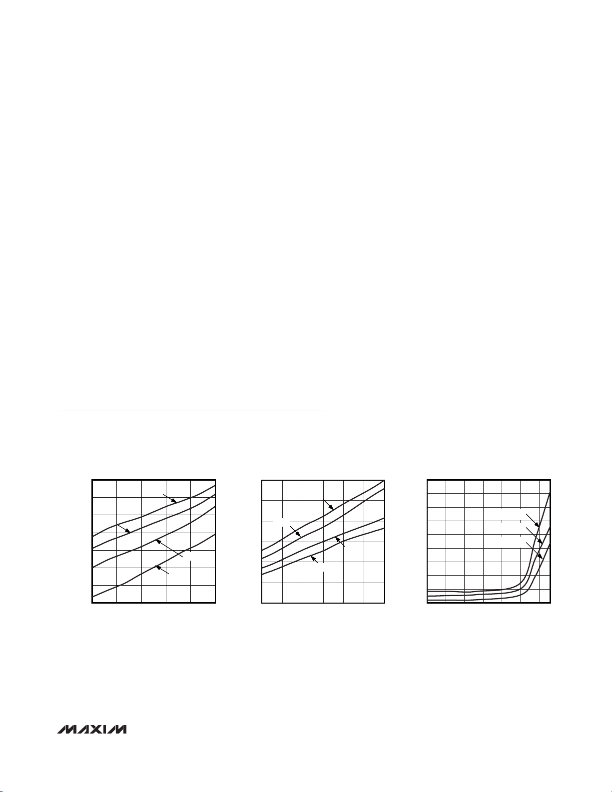
Typical Operating Characteristics
(
Typical Operating Circuit
, V
PAVDD
= V
AVDD
= V
DVDD
= V
HVIN
= +3.0V, fRF= 433.92MHz, IF BW = 280kHz. 4kbps Manchester
encoded, 0.2% BER deviation = ±50kHz, TA= +25°C, unless otherwise noted.)
SUPPLY CURRENT vs. SUPPLY VOLTAGE
MAX7031 toc01
SUPPLY VOLTAGE (V)
SUPPLY CURRENT (mA)
3.33.02.72.4
6.2
6.4
6.6
6.8
7.0
7.2
7.4
6.0
2.1 3.6
+85°C
+125°C
+25°C
-40°C
SUPPLY CURRENT vs. RF FREQUENCY
FSK MODE
MAX7030 toc02
RF FREQUENCY (MHz)
SUPPLY CURRENT (mA)
425400325 350 375
6.5
6.6
6.7
6.8
6.9
7.0
6.4
300 450
+85°C
+125°C
+25°C
-40°C
DEEP-SLEEP CURRENT vs. TEMPERATURE
MAX7031 toc03
TEMPERATURE (°C)
DEEP-SLEEP CURRENT (µA)
1108535 60-10-15
2
4
6
8
10
12
14
16
18
0
-40
VCC = +3.6V
VCC = +3.0V
VCC = +2.1V
RECEIVER
Page 6
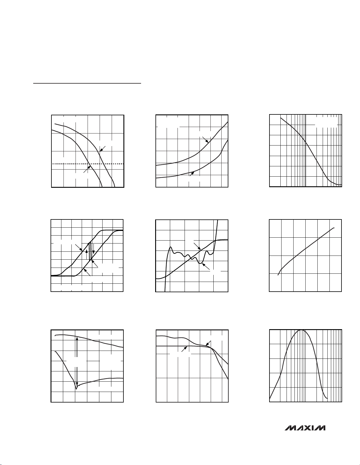
MAX7031
Low-Cost, 308MHz, 315MHz, and 433.92MHz
FSK Transceiver with Fractional-N PLL
6 _______________________________________________________________________________________
Typical Operating Characteristics (continued)
(
Typical Operating Circuit
, V
PAVDD
= V
AVDD
= V
DVDD
= V
HVIN
= +3.0V, fRF= 433.92MHz, IF BW = 280kHz. 4kbps Manchester
encoded, 0.2% BER deviation = ±50kHz, T
A
= +25°C, unless otherwise noted.)
RECEIVER
BIT-ERROR RATE
vs. AVERAGE INPUT POWER
100
280kHz IF BW
10
1
BIT-ERROR RATE (%)
0.2% BER
0.1
fRF = 315MHz
0.01
-116 -104
AVERAGE INPUT POWER (dBm)
-108 -106-110-112-114
fRF = 434MHz
MAX7031 toc04
-100
-102
-104
-106
SENSITIVITY (dBm)
-108
-110
-112
SENSITIVITY vs. TEMPERATURE
280kHz IF BW
0.2% BER
-40
TEMPERATURE (°C)
fRF = 434MHz
fRF = 315MHz
SENSITIVITY vs. FREQUENCY DEVIATION
-94
MAX7031 toc05
11085603510-15
-96
-98
-100
-102
SENSITIVITY (dBm)
-104
-106
-108
1 100
FREQUENCY DEVIATION (kHz)
10
280kHz IF BW
0.2% BER
MAX7031 toc06
1.8
1.6
1.4
HIGH-GAIN MODE
1.2
1.0
RSSI (V)
0.8
0.6
0.4
0.2
AGC HYSTERESIS: 3dB
0
-130 10
RF INPUT POWER (dBm)
AGC SWITCH
POINT
LOW-GAIN MODE
MAX7031 toc07
-10-30-70 -50-90-110
SYSTEM GAIN vs. IF FREQUENCY
50
RSSI vs. RF INPUT POWER
40
30
20
10
SYSTEM GAIN (dBm)
0
-10
-20
45dB IMAGE
REJECTION
030
IF FREQUENCY (MHz)
UPPER SIDEBAND
FROM RFIN
TO MIXOUT
= 434MHz
f
RF
LOWER SIDEBAND
252015105
MAX7031 toc10
RSSI AND DELTA vs. IF INPUT POWER
2.1
1.8
1.5
1.2
RSSI (V)
0.9
0.6
0.3
0
-90 10
IMAGE REJECTION vs. TEMPERATURE
48
46
44
IMAGE REJECTION (dB)
42
-40
RSSI
IF INPUT POWER (dBm)
fRF = 315MHz
TEMPERATURE (°C)
MAX7031 toc08
DELTA
-10-30-50-70
fRF = 434MHz
11085603510-15
3.5
2.5
1.5
0.5
-0.5
-1.5
-2.5
-3.5
MAX7031 toc11
1.6
1.2
0.8
DELTA (%)
0.4
FSK DEMODULATOR OUTPUT (V)
0
10.4 11.0
NORMALIZED IF GAIN vs. IF FREQUENCY
0
-4
-8
-12
NORMALIZED IF GAIN (dB)
-16
-20
1 100
FSK DEMODULATOR OUTPUT
vs. IF FREQUENCY
MAX7031 toc09
10.910.810.710.610.5
IF FREQUENCY (MHz)
MAX7031 toc12
10
IF FREQUENCY (MHz)
Page 7

MAX7031
Low-Cost, 308MHz, 315MHz, and 433.92MHz
ASK Transceiver with Fractional-N PLL
_______________________________________________________________________________________
7
Typical Operating Characteristics (continued)
(
Typical Operating Circuit
, V
PAVDD
= V
AVDD
= V
DVDD
= V
HVIN
= +3.0V, fRF= 433.92MHz, IF BW = 280kHz. 4kbps Manchester
encoded, 0.2% BER deviation = ±50kHz, T
A
= +25°C, unless otherwise noted.)
RECEIVER
S11 vs. RF FREQUENCY
MAX7031 toc13
RF FREQUENCY (MHz)
S11 (dB)
450400350300250
-18
-12
-6
0
-24
200 500
433.92MHz
INPUT IMPEDANCE
vs. INDUCTIVE DEGENERATION
90
fRF = 315MHz
80
IMAGINARY
70
IMPEDANCE
60
MAX7031 toc15
-220
-230
-240
-250
S11 SMITH PLOT OF RFIN
MAX7031 toc14
434MHz
400MHz
500MHz
INPUT IMPEDANCE
vs. INDUCTIVE DEGENERATION
90
80
70
60
fRF = 434MHz
IMAGINARY
IMPEDANCE
MAX7031 toc16
-150
-160
-170
-180
50
REAL IMPEDANCE (Ω)
40
30
20
1100
PHASE NOISE vs. OFFSET FREQUENCY
-50
-60
-70
-80
-90
PHASE NOISE (dBc/Hz)
-100
-110
-120
100 10M
REAL IMPEDANCE
10
INDUCTIVE DEGENERATION (nH)
fRF = 315MHz
OFFSET FREQUENCY (Hz)
-260
-270
-280
-290
50
REAL IMPEDANCE (Ω)
IMAGINARY IMPEDANCE (Ω)
40
30
20
1100
REAL IMPEDANCE
10
INDUCTIVE DEGENERATION (nH)
-190
-200
-210
-220
IMAGINARY IMPEDANCE (Ω)
PHASE NOISE vs. OFFSET FREQUENCY
-50
MAX7031 toc17
1M100k10k1k
-60
-70
-80
-90
PHASE NOISE (dBc/Hz)
-100
-110
-120
100 10M
OFFSET FREQUENCY (Hz)
fRF = 434MHz
MAX7031 toc18
1M100k10k1k
Page 8

MAX7031
Low-Cost, 308MHz, 315MHz, and 433.92MHz
FSK Transceiver with Fractional-N PLL
8 _______________________________________________________________________________________
Typical Operating Characteristics (continued)
(
Typical Operating Circuit
, V
PAVDD
= V
AVDD
= V
DVDD
= V
HVIN
= +3.0V, fRF= 433.92MHz, IF BW = 280kHz. 4kbps Manchester
encoded, 0.2% BER deviation = ±50kHz, T
A
= +25°C, unless otherwise noted.)
SUPPLY CURRENT vs. SUPPLY VOLTAGE
MAX7031 toc19
SUPPLY VOLTAGE (V)
SUPPLY CURRENT (mA)
3.33.02.72.4
10
12
14
16
8
2.1 3.6
fRF = 315MHz
TA = +85°C
TA = +125°C
TA = -40°C
TA = +25°C
SUPPLY CURRENT (mA)
11
13
15
17
9
SUPPLY CURRENT
vs. SUPPLY VOLTAGE
MAX7031 toc20
SUPPLY VOLTAGE (V)
3.33.02.72.42.1 3.6
fRF = 434MHz
TA = +85°C
TA = +125°C
TA = -40°C
TA = +25°C
SUPPLY CURRENT vs. OUTPUT POWER
MAX7031 toc21
AVERAGE OUTPUT POWER (dBm)
SUPPLY CURRENT (mA)
62-10 -6 -2
5
6
7
8
9
10
11
12
4
-14 10
fRF = 315MHz
SUPPLY CURRENT vs. OUTPUT POWER
MAX7031 toc22
AVERAGE OUTPUT POWER (dBm)
SUPPLY CURRENT (mA)
62-10 -6 -2
5
6
7
8
9
10
11
12
13
14
-14 10
fRF = 434MHz
OUTPUT POWER vs. SUPPLY VOLTAGE
MAX7031 toc 23
SUPPLY VOLTAGE (V)
OUTPUT POWER (dBm)
3.33.02.72.4
6
8
10
12
14
4
2.1 3.6
fRF = 315MHz
TA = +85°C
TA = +125°C
TA = +25°C
TA = -40°C
OUTPUT POWER (dBm)
6
8
10
12
14
4
OUTPUT POWER vs. SUPPLY VOLTAGE
MAX7030 toc24
SUPPLY VOLTAGE (V)
3.33.02.72.42.1 3.6
TA = +85°C
TA = +125°C
TA = +25°C
TA = -40°C
fRF = 434MHz
EFFICIENCY vs. SUPPLY VOLTAGE
MAX7031 toc25
SUPPLY VOLTAGE (V)
EFFFICIENCY (%)
3.33.02.72.4
25
30
35
40
20
2.1 3.6
TA = +85°C
TA = +125°C
TA = +25°C
TA = -40°C
fRF = 315MHz
EFFICIENCY vs. SUPPLY VOLTAGE
MAX7031 toc26
SUPPLY VOLTAGE (V)
EFFFICIENCY (%)
3.33.02.72.4
25
30
35
40
20
2.1 3.6
TA = +85°C
TA = +125°C
TA = +25°C
TA = -40°C
fRF = 434MHz
TRANSMITTER
Page 9

MAX7031
Low-Cost, 308MHz, 315MHz, and 433.92MHz
ASK Transceiver with Fractional-N PLL
_______________________________________________________________________________________
9
Typical Operating Characteristics (continued)
(
Typical Operating Circuit
, V
PAVDD
= V
AVDD
= V
DVDD
= V
HVIN
= +3.0V, fRF= 433.92MHz, IF BW = 280kHz. 4kbps Manchester
encoded, 0.2% BER deviation = ±50kHz, TA= +25°C, unless otherwise noted.)
TRANSMITTER
PHASE NOISE vs. OFFSET FREQUENCY
(TRANSMIT MODE)
-40
fRF = 315MHz
-50
-60
-70
-80
-90
-100
PHASE NOISE (dBc/Hz)
-110
-120
-130
-140
100 10M
OFFSET FREQUENCY (Hz)
REFERENCE SPUR MAGNITUDE
vs. SUPPLY VOLTAGE
-40
-45
-50
-55
-60
-65
REFERENCE SPUR MAGNITUDE (dBc)
-70
2.1 3.6
434MHz
315MHz
SUPPLY VOLTAGE (V)
MAX7031 toc27
1M100k10k1k
MAX7031 toc29
3.33.02.72.4
PHASE NOISE vs. OFFSET FREQUENCY
(TRANSMIT MODE)
-40
fRF = 434MHz
-50
-60
-70
-80
-90
-100
PHASE NOISE (dBc/Hz)
-110
-120
-130
-140
OFFSET FREQUENCY (Hz)
FREQUENCY STABILITY
vs. SUPPLY VOLTAGE
10
8
6
4
2
0
-2
-4
FREQUENCY STABILITY (ppm)
-6
-8
-10
fRF = 315MHz
fRF = 434MHz
SUPPLY VOLTAGE (V)
MAX7031 toc28
1M100k10k1k100 10M
MAX7031 toc30
3.33.02.72.42.1 3.6
Page 10

MAX7031
Low-Cost, 308MHz, 315MHz, and 433.92MHz
FSK Transceiver with Fractional-N PLL
10 ______________________________________________________________________________________
Pin Description
PIN NAME FUNCTION
1 PAVDD
2ROUT
3 TX/RX1
4 TX/RX2 Transmit/Receive Switch Pole. Typically connected to ground. See the Typical Application Circuit.
5 PAOUT
6 AVDD
7 LNAIN Low-Noise Amplifier Input. Must be AC-coupled.
8 LNASRC
9 LNAOUT
10 MIXIN+ Noninverting Mixer Input. Must be AC-coupled to the LNA output.
11 MIXIN- Inverting Mixer Input. Bypass to AVDD with a capacitor as close as possible to the LNA LC tank filter.
12 MIXOUT 330Ω Mixer Output. Connect to the input of the 10.7MHz filter.
13 IFIN- Inverting 330Ω IF Limiter Amplifier Input. Bypass to GND with a capacitor.
14 IFIN+ Noninverting 330Ω IF Limiter Amplifier Input. Connect to the output of the 10.7MHz IF filter.
15 PDMIN Minimum-Level Peak Detector for Demodulator Output
16 PDMAX Maximum-Level Peak Detector for Demodulator Output
17 DS- Inverting Data Slicer Input
18 DS+ Noninverting Data Slicer Input
19 OP+ Noninverting Op-Amp Input for the Sallen-Key Data Filter
20 DF Data-Filter Feedback Node. Input for the feedback capacitor of the Sallen-Key data filter.
21 RSSI Buffered Received-Signal-Strength-Indicator Output
22 T/R
23 ENABLE
24 DATA Receiver Data Output/Transmitter Data Input
25 N.C. No Connection. Do not connect to this pin.
26 DVDD
27 HVIN
Power-Amplifier Supply Voltage. Bypass to GND with 0.01µF and 220pF capacitors placed as close
as possible to the pin.
Envelope-Shaping Output. ROUT controls the power-amplifier envelope’s rise and fall times. Connect
ROUT to the PA pullup inductor or optional power-adjust resistor. Bypass the inductor to GND as
close as possible to the inductor with 680pF and 220pF capacitors as shown in the Typical
Application Circuit.
Transmit/Receive Switch Throw. Drive T/R high to short TX/RX1 to TX/RX2. Drive T/R low to disconnect
TX/RX1 from TX/RX2. Functionally identical to TX/RX2.
Power-Amplifier Output. Requires a pullup inductor to the supply voltage (or ROUT if envelope
shaping is desired), which can be part of the output-matching network to an antenna.
Analog Power-Supply Voltage. AVDD is connected to an on-chip +3.0V regulator in 5V operation.
Bypass AVDD to GND with a 0.1µF and 220pF capacitor placed as close as possible to the pin.
Low-Noise Amplifier Source for External Inductive Degeneration. Connect an inductor to GND to set
the LNA input impedance.
Low-Noise Amplifier Output. Must be connected to AVDD through a parallel LC tank filter. AC-couple
to MIXIN+.
Transmit/Receive. Drive high to put the device in transmit mode. Drive low or leave unconnected to
put the device in receive mode. It is internally pulled down.
Enable. Drive high for normal operation. Drive low or leave unconnected to put the device into
shutdown mode.
Digital Power-Supply Voltage. Bypass to GND with a 0.01µF and 220pF capacitor placed as close as
possible to the pin.
High-Voltage Supply Input. For 3V operation, connect HVIN to AVDD, PAVDD, and DVDD. For 5V
operation, connect only HVIN to 5V. Bypass HVIN to GND with a 0.01µF and 220pF capacitor placed
as close as possible to the pin.
Page 11

MAX7031
Low-Cost, 308MHz, 315MHz, and 433.92MHz
FSK Transceiver with Fractional-N PLL
______________________________________________________________________________________ 11
Detailed Description
The MAX7031 308MHz, 315MHz, and 433.92MHz
CMOS transceiver and a few external components provide a complete transmit and receive chain from the
antenna to the digital data interface. This device is
designed for transmitting and receiving FSK data. All
transmit frequencies are generated by a fractional-Nbased synthesizer, allowing for very fine frequency
steps in increments of f
XTAL
/4096. The receive local
oscillator (LO) is generated by a traditional integer-Nbased synthesizer. Depending on component selection, data rates as high as 33kbps (Manchester
encoded) or 66kbps (NRZ encoded) can be achieved.
Receiver
Low-Noise Amplifier (LNA)
The LNA is a cascode amplifier with off-chip inductive
degeneration that achieves approximately 30dB of voltage gain that is dependent on both the antenna-matching network at the LNA input, and the LC tank network
between the LNA output and the mixer inputs.
The off-chip inductive degeneration is achieved by connecting an inductor from LNASRC to AGND. This inductor sets the real part of the input impedances at LNAIN,
allowing for a more flexible match for low-input impedances such as a PCB trace antenna. A nominal value
for this inductor with a 50Ω input impedance is 12nH at
315MHz and 10nH at 434MHz, but the inductance is
affected by PCB trace length. LNASRC can be shorted
to ground to increase sensitivity by approximately 1dB,
but the input match must then be reoptimized.
The LC tank filter connected to LNAOUT consists of L5
and C9 (see the
Typical Application Circuit
). Select L5
and C9 to resonate at the desired RF input frequency.
The resonant frequency is given by:
where L
TOTAL
= L5 + L
PARASITICS
and C
TOTAL
= C9 +
C
PARASITICS
.
L
PARASITICS
and C
PARASITICS
include inductance and
capacitance of the PCB traces, package pins, mixer
input impedance, LNA output impedance, etc. These
parasitics at high frequencies cannot be ignored, and
can have a dramatic effect on the tank filter center frequency. Lab experimentation should be done to optimize the center frequency of the tank. The parasitic
capacitance is generally 5pF to 7pF.
Automatic Gain Control (AGC)
When the AGC is enabled, it monitors the RSSI output.
When the RSSI output reaches 1.28V, which corresponds to an RF input level of approximately -55dBm,
the AGC switches on the LNA gain-reduction attenuator. The attenuator reduces the LNA gain by 36dB,
thereby reducing the RSSI output by about 540mV to
740mV. The LNA resumes high-gain mode when the
RSSI output level drops back below 680mV (approximately -59dBm at the RF input) for a programmable
interval called the AGC dwell time (see Table 1). The
AGC has a hysteresis of approximately 4dB. With the
AGC function, the RSSI dynamic range is increased.
AGC is not necessary for most FSK applications.
AGC Dwell Time Settings
The AGC dwell timer holds the AGC in a low-gain state
for a set amount of time after the power level drops
below the AGC switching threshold. After that set
amount of time, if the power level is still below the AGC
threshold, the LNA goes into high-gain state.
Pin Description (continued)
PIN NAME FUNCTION
28 AUTOCAL Enable (Logic-High) to Allow FSK Demodulator Calibration. Bypass to GND with a 10pF capacitor.
29 AGC1 AGC Enable/Dwell Time Control 1. See Table 1. Bypass to GND with a 10pF capacitor.
30 AGC0 AGC Enable/Dwell Time Control 0 (LSB). See Table 1. Bypass to GND with a 10pF capacitor.
31 XTAL1 Crystal Input 1. Bypass to GND if XTAL2 is driven by an AC-coupled external reference.
32 XTAL2 Crystal Input 2. XTAL2 can be driven from an external AC-coupled reference.
— EP Exposed Pad. Solder evenly to the board’s ground plane for proper operation.
f
=
LC
2π
1
×
TOTAL TOTAL
Page 12

MAX7031
Low-Cost, 308MHz, 315MHz, and 433.92MHz
FSK Transceiver with Fractional-N PLL
12 ______________________________________________________________________________________
The MAX7031 uses the two AGC control pins (AGC0
and AGC1) to enable or disable the AGC and set three
user-controlled dwell timer settings. The AGC dwell
time is dependent on the crystal frequency and the bit
settings of the AGC control pins. To calculate the dwell
time, use the following equation:
where K is an integer in decimal, determined by the
control pin settings shown in Table 1.
For example, a receiver operating at 315MHz has a
crystal oscillator frequency of 12.679MHz. For K = 11
(AGC setting = 0, 1), the dwell timer is 162µs; for K =
14 (AGC setting = 1, 0), the dwell timer is 1.3ms; for K
= 20 (AGC setting = 1, 1), the dwell time is 83ms.
Mixer
A unique feature of the MAX7031 is the integrated
image rejection of the mixer. This eliminates the need
for a costly front-end SAW filter for many applications.
The advantage of not using a SAW filter is increased
sensitivity, simplified antenna matching, less board
space, and lower cost.
The mixer cell is a pair of double-balanced mixers that
perform an IQ downconversion of the RF input to the
10.7MHz intermediate frequency (IF) with low-side
injection (i.e., f
LO
= fRF- fIF). The image-rejection circuit
then combines these signals to achieve a typical 46dB
of image rejection over the full temperature range. Lowside injection is required as high-side injection is not
possible due to the on-chip image rejection. The IF output is driven by a source follower, biased to create a
driving impedance of 330Ω to interface with an off-chip
330Ω ceramic IF filter. The voltage conversion gain driving a 330Ω load is approximately 20dB. Note that the
MIXIN+ and MIXIN- inputs are functionally identical.
Integer-N, Phase-Locked Loop (PLL)
The MAX7031 utilizes a fixed integer-N PLL to generate
the receive LO. All PLL components, including the loop
filter, voltage-controlled oscillator, charge pump, asynchronous 24x divider, and phase-frequency detector
are internal. The loop bandwidth is approximately
500kHz. The relationship between RF, IF, and reference
frequencies is given by:
f
REF
= (f
RF
- fIF)/24
Intermediate Frequency (IF)
The IF section presents a differential 330Ω load to provide matching for the off-chip ceramic filter. The internal
six AC-coupled limiting amplifiers produce an overall
gain of approximately 65dB, with a bandpass filter-type
response centered near the 10.7MHz IF frequency with
a 3dB bandwidth of approximately 10MHz. The RSSI
circuit demodulates the IF to baseband by producing a
DC output proportional to the log of the IF signal level
with a slope of approximately 15mV/dB.
FSK Demodulator
The FSK demodulator uses an integrated 10.7MHz PLL
that tracks the input RF modulation and converts the
frequency deviation into a voltage difference. The PLL
is illustrated in Figure 1. The input to the PLL comes
from the output of the IF limiting amplifiers. The PLL
control voltage responds to changes in the frequency
of the input signal with a nominal gain of 2.0mV/kHz.
For example, an FSK peak-to-peak deviation of 50kHz
Figure 1. FSK Demodulator PLL Block Diagram
Figure 2. Sallen-Key Lowpass Data Filter
Table 1. AGC Dwell Time Settings for
MAX7031
AGC1 AGC0 DESCRIPTION
0 0 AGC disabled, high gain selected
01 K = 11, short dwell time
10 K = 14, medium dwell time
11 K = 20, long dwell time
K
Dwell Time
=
2
f
XTAL
100kΩ
C
FSK
DEMOD
F2
TO FSK BASEBAND FILTER
PHASE
IF
LIMITING
AMPS
DETECTOR
CHARGE
PUMP
LOOP
FILTER
AND DATA SLICER
10.7MHz VCO
2.0mV/kHz
MAX7031
DFOP+DS+
100kΩ
C
F1
Page 13

MAX7031
Low-Cost, 308MHz, 315MHz, and 433.92MHz
FSK Transceiver with Fractional-N PLL
______________________________________________________________________________________ 13
generates a 100mV
P-P
signal on the control line. This
control voltage is then filtered and sliced by the baseband circuitry.
The FSK demodulator PLL requires calibration to overcome variations in process, voltage, and temperature.
This is done by cycling the ENABLE pin when the
AUTOCAL pin is a logic 1. If the AUTOCAL pin is a
logic 0, calibration cannot occur.
Data Filter
The data filter for the demodulated data is implemented
as a 2nd-order, lowpass Sallen-Key filter. The pole
locations are set by the combination of two on-chip
resistors and two external capacitors. Adjusting the
value of the external capacitors changes the corner frequency to optimize for different data rates. Set the corner frequency in kHz to approximately 2 times the
fastest expected Manchester data rate in kbps from the
transmitter (1.0 times the fastest expected NRZ data
rate). Keeping the corner frequency near the data rate
rejects any noise at higher frequencies, resulting in an
increase in receiver sensitivity.
The configuration shown in Figure 2 can create a
Butterworth or Bessel response. The Butterworth filter
offers a very-flat-amplitude response in the passband
and a rolloff rate of 40dB/decade for the two-pole filter.
The Bessel filter has a linear phase response, which
works well for filtering digital data. To calculate the
value of the capacitors, use the following equations,
along with the coefficients in Table 2:
where fCis the desired 3dB corner frequency.
For example, choose a Butterworth filter response with
a corner frequency of 5kHz:
Choosing standard capacitor values changes CF1to
470pF and CF2to 220pF. In the
Typical Application
Circuit
, CF1and CF2are named C16 and C17,
respectively.
Table 2. Coefficients to Calculate C
F1
and C
F2
Figure 3. Generating Data Slicer Threshold Using a Lowpass
Filter
Figure 4. Generating Data Slicer Threshold Using the Peak
Detectors
MAX7031
DATA
SLICER
DATA
DS- DS+
R
C
FILTER TYPE a b
Butterworth
(Q = 0.707)
Bessel
(Q = 0.577)
1.414 1.000
1.3617 0.618
MAX7031
PEAK
DATA
SLICER
DATA
DET
PDMAX PDMIN
R
C
PEAK
DET
R
C
C
=
1
F
=
C
2
F
b
100
Ω
()()()
ak f
π
c
a
4 100
Ω
()()()
π
kf
c
1 000
C
=≈
FF1
1 414 100 3 14 5
( . )( )( . )( )
C
=≈
2
4 100 3 14 5
( )( )( . )( )
.
k kHz
Ω
1 414
.
k kHz
Ω
225
450
pF
pF
Page 14

MAX7031
Low-Cost, 308MHz, 315MHz, and 433.92MHz
FSK Transceiver with Fractional-N PLL
14 ______________________________________________________________________________________
Data Slicer
The data slicer takes the analog output of the data filter
and converts it to a digital signal. This is achieved by
using a comparator and comparing the analog input to
a threshold voltage. The threshold voltage is set by the
voltage on the DS- pin, which is connected to the negative input of the data-slicer comparator.
Numerous configurations can be used to generate the
data-slicer threshold. For example, the circuit in Figure
3 shows a simple method using only one resistor and
one capacitor. This configuration averages the analog
output of the filter and sets the threshold to approximately 50% of that amplitude. With this configuration,
the threshold automatically adjusts as the analog signal
varies, minimizing the possibility for errors in the digital
data. The values of R and C affect how fast the threshold tracks the analog amplitude. Be sure to keep the
corner frequency of the RC circuit much lower (about
10 times) than the lowest expected data rate.
With this configuration, a long string of NRZ zeros or
ones can cause the threshold to drift. This configuration
works best if a coding scheme, such as Manchester
coding, which has an equal number of zeros and ones,
is used.
Figure 4 shows a configuration that uses the positive and
negative peak detectors to generate the threshold. This
configuration sets the threshold to the midpoint between
a high output and a low output of the data filter.
Peak Detectors
The maximum peak detector (PDMAX) and minimum
peak detector (PDMIN), with resistors and capacitors
shown in Figure 4, create DC output voltages equal to
the high- and low-peak values of the filtered demodulated signal. The resistors provide a path for the capacitors to discharge, allowing the peak detectors to
dynamically follow peak changes of the data filter output voltages.
The maximum and minimum peak detectors can be
used together to form a data slicer threshold voltage at
a value midway between the maximum and minimum
voltage levels of the data stream (see the
Data Slicer
section and Figure 4). Set the RC time constant of the
peak-detector combining network to at least 5 times the
data period.
If there is an event that causes a significant change in
the magnitude of the baseband signal, such as an AGC
gain switch or a power-up transient, the peak detectors
may “catch” a false level. If a false peak is detected,
the slicing level is incorrect. The MAX7031 peak detectors correct these problems by temporarily tracking the
incoming baseband filter voltage when an AGC state
switch occurs, or by forcing the peak detectors to track
the baseband filter output voltage until all internal circuits are stable following an enable pin low-to-high
transition. The peak detectors exhibit a fast attack/slow
decay response. This feature allows for an extremely
fast startup or AGC recovery.
Transmitter
Power Amplifier (PA)
The PA of the MAX7031 is a high-efficiency, opendrain, switch-mode amplifier. The PA with proper output- matching network can drive a wide range of
antenna impedances, which includes a small-loop PCB
trace and a 50Ω antenna. The output-matching network
for a 50Ω antenna is shown in the
Typical Application
Circuit
. The output-matching network suppresses the
carrier harmonics and transforms the antenna impedance to an optimal impedance at PAOUT (pin 5). The
optimal impedance at PAOUT is 250Ω.
When the output-matching network is properly tuned,
the PA transmits power with a high overall efficiency of
up to 32%. The efficiency of the PA itself is more than
46%. The output power is set by an external resistor at
PAOUT, and is also dependent on the external antenna
and antenna-matching network at the PA output.
Envelope Shaping
The MAX7031 features an internal envelope-shaping
resistor, which connects between the open-drain output
of the PA and the power supply. The envelope-shaping
resistor slows the turn-on/turn-off of the PA. Envelope
shaping is not necessary for FSK. For most applications, the PA pullup inductor should be connected to
PAVDD instead of ROUT.
Fractional-N Phase-Locked Loop (PLL)
The MAX7031 utilizes a fully integrated, fractional-N
PLL for its transmit frequency synthesizer. All PLL components, including the loop filter, are integrated internally. The loop bandwidth is approximately 200kHz.
Power-Supply Connections
The MAX7031 can be powered from a 2.1V to 3.6V supply or a 4.5V to 5.5V supply. If a 4.5V to 5.5V supply is
used, then the on-chip linear regulator reduces the 5V
supply to the 3V needed to operate the chip.
To operate the MAX7031 from a 3V supply, connect
PAVDD, AVDD, DVDD, and HVIN to the 3V supply.
When using a 5V supply, connect the supply to HVIN
only and connect AVDD, PAVDD, and DVDD together.
In both cases, bypass PAVDD, DVDD, and HVIN to
GND with a 0.01µF and 220pF capacitor and bypass
AVDD to GND with a 0.1µF and 220pF capacitor.
Page 15

Bypass T/R, ENABLE, DATA, AGC0-1, and AUTOCAL
with 10pF capacitors to GND. Place all bypass capacitors as close to the respective pins as possible.
Transmit/Receive Antenna Switch
The MAX7031 features an internal SPST RF switch that,
when combined with a few external components, allows
the transmit and receive pins to share a common antenna (see the
Typical Application Circuit)
. In receive
mode, the switch is open and the power amplifier is
shut down, presenting a high impedance to minimize
the loading of the LNA. In transmit mode, the switch
closes to complete a resonant tank circuit at the PA output and forms an RF short at the input to the LNA. In
this mode, the external passive components couple the
output of the PA to the antenna to protect the LNA input
from strong transmitted signals.
The switch state is controlled by the T/R pin (pin 22).
Drive T/R high to put the device in transmit mode; drive
T/R low to put the device in receive mode.
Crystal Oscillator (XTAL)
The XTAL oscillator in the MAX7031 is designed to present a capacitance of approximately 3pF between the
XTAL1 and XTAL2 pins. In most cases, this corresponds to a 4.5pF load capacitance applied to the
external crystal when typical PCB parasitics are added.
It is very important to use a crystal with a load
capacitance that is equal to the capacitance of the
MAX7031 crystal oscillator plus PCB parasitics. If a
crystal designed to oscillate with a different load
capacitance is used, the crystal is pulled away from its
stated operating frequency, introducing an error in the
reference frequency. Crystals designed to operate with
higher differential load capacitance always pull the reference frequency higher.
In actuality, the oscillator pulls every crystal. The crystal’s natural frequency is really below its specified frequency, but when loaded with the specified load
capacitance, the crystal is pulled and oscillates at its
specified frequency. This pulling is already accounted
for in the specification of the load capacitance.
Additional pulling can be calculated if the electrical
parameters of the crystal are known. The frequency
pulling is given by:
where:
f
P
is the amount the crystal frequency is pulled in ppm.
Cm is the motional capacitance of the crystal.
C
CASE
is the case capacitance.
C
SPEC
is the specified load capacitance.
C
LOAD
is the actual load capacitance.
When the crystal is loaded as specified, i.e., C
LOAD
=
C
SPEC
, the frequency pulling equals zero.
MAX7031
Low-Cost, 308MHz, 315MHz, and 433.92MHz
FSK Transceiver with Fractional-N PLL
______________________________________________________________________________________ 15
Pin Configuration
Chip Information
PROCESS: CMOS
⎛
C
m
f
=
P
⎜
2
CC CC
⎝
11
+
CASE LOAD CASE SPEC
−
+
⎞
10
x
⎟
⎠
TOP VIEW
DATA
ENABLE
T/R
N.C.
DVDD
HVIN
AUTOCAL
AGC1
AGC0
XTAL1
XTAL2
RSSIDFOP+
25
26
27
28
29
30
31
32
+
1
MAX7031
4
3
2
5
DS+17DS-
18192021222324
PDMAX
16
15
PDMIN
14
IFIN+
13
IFIN-
12
MIXOUT
11
MIXIN-
10
MIXIN+
9
LNAOUT
7
8
6
6
ROUT
PAVDD
TX/RX1
THIN QFN
TX/RX2
AVDD
LNAIN
PAOU T
LNASRC
Page 16

MAX7031
Low-Cost, 308MHz, 315MHz, and 433.92MHz
FSK Transceiver with Fractional-N PLL
16 ______________________________________________________________________________________
/
Typical Application Circuit
Selector Guide
+
Denotes a lead(Pb)-free/RoHS-compliant package.
†
Contact factory for availability.
C1C2
L2
C4
C8
*OPTIONAL POWER-ADJUST RESISTOR
AGC0
AGC1
C17
AUTOCAL
DATA
ENABLE
TRANSMIT
RECEIVE
C16
R3*
C3
C5
V
DD
C21
Y1
XTAL2
LNAOUT
910
XTAL1
MIXIN+
C10
C20
L5
C11
16
N.C.
DATA
ENABLE
RSSI
PDMAX
T/R
OP+
DS+
DS-
C15
C19
24
23
22
21
20
DF
19
18
17
R1
R2
C18
25262728293032 31
HVIN
AGC0
AGC1
AUTOCAL
DVDD
MAX7031
EXPOSED
PAD
MIXIN-
11
12
C12
V
C9
DD
MIXOUT
C13
IN OUTGND
IFIN-
13
14
Y2
IFIN+
PDMIN
15
C14
V
DD
3.0V
C23
C24
L1
C7
L3
C22
V
DD
1
PAVDD
2
ROUT
3
TX/RX1
4
TX/RX2
5
PAOUT
V
DD
6
C6
L6
AVDD
7
LNAIN
8
LNASRC
L4
PART
M AX 7031LATJ+
†
M AX 7031M ATJ15+ 315 ±15.477
M AX 7031M ATJ50+ 315 ±49.528
M AX 7031H ATJ17+ 433.92 ±17.221
M AX 7031H ATJ51+ 433.92 ±51.663
CARRIER
F R EQ U EN C Y ( M H z)
308 ±51.413
FSK DEVIATION
F R EQ U EN C Y ( k H z)
Page 17

MAX7031
Low-Cost, 308MHz, 315MHz, and 433.92MHz
FSK Transceiver with Fractional-N PLL
______________________________________________________________________________________ 17
MAX7031
Table 3. Component Values for Typical Application Circuit
Note: Component values vary depending on PCB layout.
COMPONENT
C1 220pF 220pF 10%
C2 680pF 680pF 10%
C3 6.8pF 12pF 5%
C4 6.8pF 10pF 5%
C5 10pF 22pF 5%
C6 220pF 220pF 10%
C7 0.1µF 0.1µF 10%
C8 100pF 100pF 5%
C9 1.8pF 2.7pF ±0.1pF
C10 100pF 100pF 5%
C11 220pF 220pF 10%
C12 100pF 100pF 5%
C13 1500pF 1500pF 10%
C14 0.047µF 0.047µF 10%
C15 0.047µF 0.047µF 10%
C16 470pF 470pF 10%
C17 220pF 220pF 10%
C18 220pF 220pF 10%
C19 0.01µF 0.01µF 10%
C20 100pF 100pF 5%
C21 100pF 100pF 5%
C22 220pF 220pF 10%
C23 0.01µF 0.01µF 10%
C24 0.01µF 0.01µF 10%
L1 22nH 27nH Coilcraft 0603CS
L2 22nH 30nH Coilcraft 0603CS
L3 22nH 30nH Coilcraft 0603CS
L4 10nH 12nH Coilcraft 0603CS
L5 16nH 30nH Murata LQW18A
L6 68nH 100nH Coilcraft 0603CS
R1 100kΩ 100kΩ 5%
R2 100kΩ 100kΩ 5%
R3 0Ω 0Ω —
Y1 17.63416MHz 12.67917MHz
Y2 10.7MHz ceramic filter 10.7MHz ceramic filter Murata SFECV10.7 series
VALUE FOR
433.92MHz RF
VALUE FOR
315MHz RF
DESCRIPTION
Crystal, 4.5pF load
capacitance
Page 18

MAX7031
Low-Cost, 308MHz, 315MHz, and 433.92MHz
FSK Transceiver with Fractional-N PLL
18 ______________________________________________________________________________________
Functional Diagram
7
LNAIN
LNASRC
8
XTAL1
31
OSCILLATOR
XTAL2
32
HVIN
27
AVDD
6
LNA
CRYSTAL
REGULATOR
MIXIN-MIXIN+LNAOUT
9 10 11 12
0°
90°
I
Q
RX VCO
RX
FREQUENCY
DIVIDER
PHASE
DETECTOR
CHARGE
PUMP
3.0V
LOOP FILTER
Σ
TX
FREQUENCY
DIVIDER
TX VCO
IFIN+ IFIN-MIXOUT
14
13
IF LIMITING
RSSI
∆Σ
MODULATOR
AMPS
FSK
DEMODULATOR
DATA FILTER
100kΩ
RX
DATA
100kΩ
DF
20
19
OP+
21
RSSI
18
DS+
PDMIN
15
PDMAX
16
DS-
17
EXPOSED
PAD
ROUT PAVDD PAOUT T/R DVDD ENABLE
MAX7031
12
PA
5
TX/RX1 TX/RX2
DIGITAL LOGIC
23
3
4
26
22
30
29
28
24
AGC0
AGC1
AUTOCAL
DATA
Page 19

MAX7031
Low-Cost, 308MHz, 315MHz, and 433.92MHz
FSK Transceiver with Fractional-N PLL
______________________________________________________________________________________ 19
PACKAGE TYPE PACKAGE CODE OUTLINE NO. LAND PATTERN NO.
32 TQFN-EP T3255+3
21-0140 90-0001
Package Information
For the latest package outline information and land patterns, go to www.maxim-ic.com/packages. Note that a “+”, “#”, or “-” in the
package code indicates RoHS status only. Package drawings may show a different suffix character, but the drawing pertains to the
package regardless of RoHS status.
Page 20

MAX7031
Low-Cost, 308MHz, 315MHz, and 433.92MHz
FSK Transceiver with Fractional-N PLL
Maxim cannot assume responsibility for use of any circuitry other than circuitry entirely embodied in a Maxim product. No circuit patent licenses are
implied. Maxim reserves the right to change the circuitry and specifications without notice at any time.
20
____________________Maxim Integrated Products, 120 San Gabriel Drive, Sunnyvale, CA 94086 408-737-7600
© 2010 Maxim Integrated Products Maxim is a registered trademark of Maxim Integrated Products, Inc.
Revision History
REVISION
NUMBER
0 5/05 Initial release —
1 9/08
2 6/09 Made correction in Power Amplifer (PA) section 14
3 11/10 Updated AUTOCAL pin function description and FSK Demodulator section 11, 12
REVISION
DATE
DESCRIPTION
Added + to each part to denote lead-free/RoHS-compliant package and explicitly
calling out the odd frequency as contact factory for availability
PAGES
CHANGED
16
 Loading...