MAXIM MAX7030 Technical data
General Description
The MAX7030 crystal-based, fractional-N transceiver is
designed to transmit and receive ASK/OOK data at factory-preset carrier frequencies of 315MHz, 345MHz†, or
433.92MHz with data rates up to 33kbps (Manchester
encoded) or 66kbps (NRZ encoded). This device generates a typical output power of +10dBm into a 50Ω
load and exhibits typical sensitivity of -114dBm. The
MAX7030 features separate transmit and receive pins
(PAOUT and LNAIN) and provides an internal RF switch
that can be used to connect the transmit and receive
pins to a common antenna.
The MAX7030 transmit frequency is generated by a 16bit, fractional-N, phase-locked loop (PLL), while the
receiver’s local oscillator (LO) is generated by an integer-N PLL. This hybrid architecture eliminates the need
for separate transmit and receive crystal reference
oscillators because the fractional-N PLL is preset to be
10.7MHz above the receive LO. Retaining the fixed-N
PLL for the receiver avoids the higher current-drain
requirements of a fractional-N PLL and keeps the
receiver current drain as low as possible. All frequencygeneration components are integrated on-chip, and
only a crystal, a 10.7MHz IF filter, and a few discrete
components are required to implement a complete
antenna/digital data solution.
The MAX7030 is available in a small, 5mm x 5mm, 32pin thin QFN package, and is specified to operate over
the automotive -40°C to +125°C temperature range.
Applications
2-Way Remote Keyless Entry
Security Systems
Home Automation
Remote Controls
Remote Sensing
Smoke Alarms
Garage Door Openers
Local Telemetry Systems
Features
o +2.1V to +3.6V or +4.5V to +5.5V Single-Supply
Operation
o Single-Crystal Transceiver
o Factory-Preset Frequency (No Serial Interface
Required)
o ASK/OOK Modulation
o +10dBm Output Power into 50Ω Load
o Integrated TX/RX Switch
o Integrated Transmit and Receive PLL, VCO, and
Loop Filter
o > 45dB Image Rejection
o Typical RF Sensitivity*: -114dBm
o Selectable IF Bandwidth with External Filter
o < 12.5mA Transmit-Mode Current
o < 6.7mA Receive-Mode Current
o < 800nA Shutdown Current
o Fast-On Startup Feature, < 250µs
o Small, 32-Pin, Thin QFN Package
MAX7030
Low-Cost, 315MHz, 345MHz, and 433.92MHz
ASK Transceiver with Fractional-N PLL
________________________________________________________________
Maxim Integrated Products
1
Ordering Information
19-3706; Rev 3; 11/10
For pricing, delivery, and ordering information, please contact Maxim Direct at 1-888-629-4642,
or visit Maxim’s website at www.maxim-ic.com.
Product Selector Guide
*
0.2% BER, 4kbps Manchester-encoded data, 280kHz IF BW
+
Denotes a lead(Pb)-free/RoHS-compliant package.
**
EP = Exposed pad.
Note: The MAX7030 is available with factory-preset operating
frequencies. See the
Product Selector Guide
for complete part
numbers.
Pin Configuration, Typical Application Circuit, and
Functional Diagram appear at end of data sheet.
†
Contact factory for availability.
†
345
PART TEMP RANGE PIN-PACKAGE
MAX7030_ATJ+ -40°C to +125°C 32 Thin QFN-EP**
PART CARRIER FREQUENCY (MHz)
MAX7030LATJ+ 315
MAX7030MATJ+
MAX7030HATJ+ 433.92
MAX7030
Low-Cost, 315MHz, 345MHz, and 433.92MHz
ASK Transceiver with Fractional-N PLL
2 _______________________________________________________________________________________
ABSOLUTE MAXIMUM RATINGS
Stresses beyond those listed under “Absolute Maximum Ratings” may cause permanent damage to the device. These are stress ratings only, and functional
operation of the device at these or any other conditions beyond those indicated in the operational sections of the specifications is not implied. Exposure to
absolute maximum rating conditions for extended periods may affect device reliability.
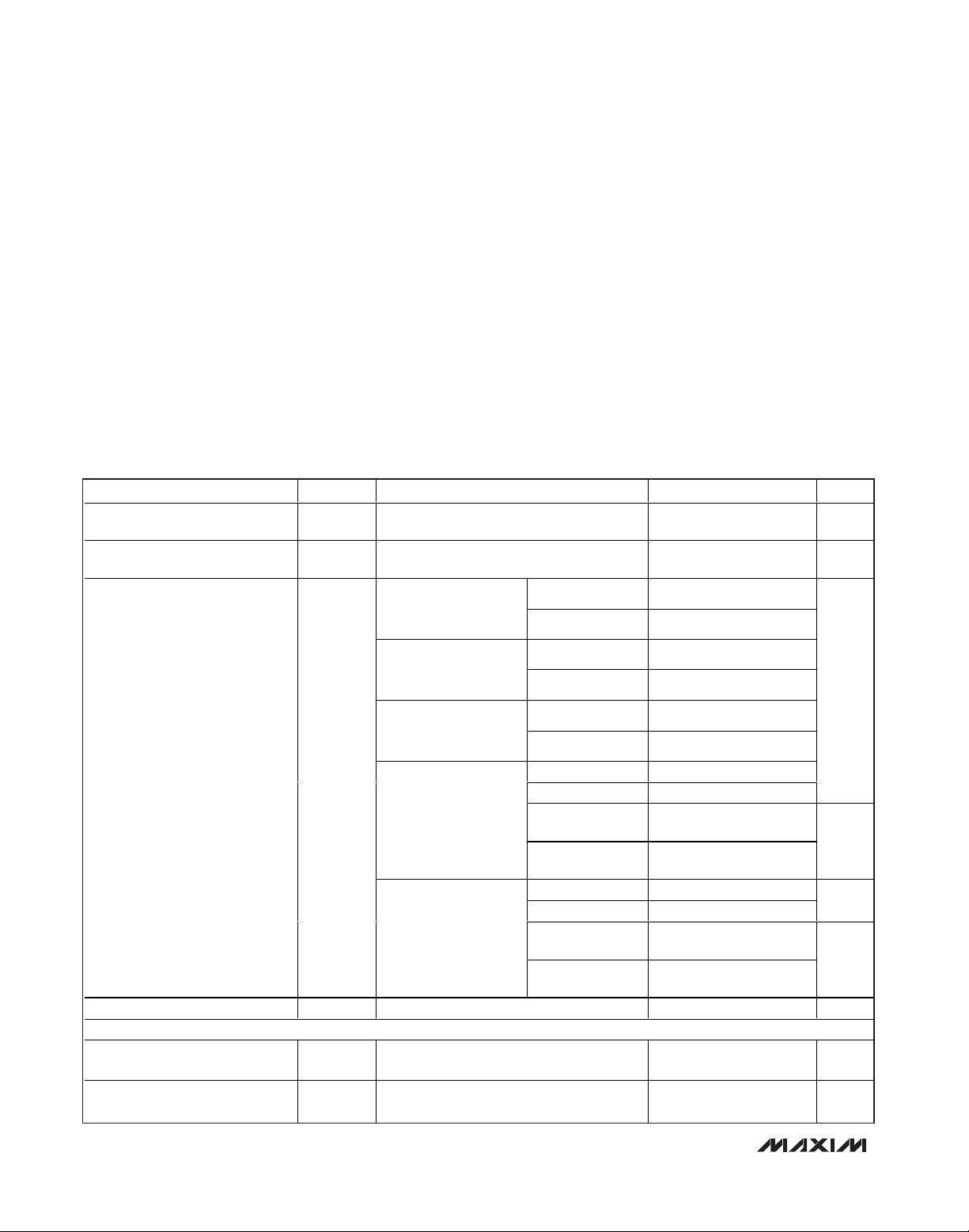
HVIN to GND .........................................................-0.3V to +6.0V
PAVDD, AVDD, DVDD to GND..............................-0.3V to +4.0V
ENABLE, T/R, DATA, AGC0, AGC1,
AGC2 to GND .......................................-0.3V to (V
HVIN
+ 0.3V)
All Other Pins to GND .............................-0.3V to (V
_VDD
+ 0.3V)
Continuous Power Dissipation (T
A
= +70°C)
32-Pin Thin QFN (derate 21.3mW/°C
above +70°C).............................................................1702mW
Operating Temperature Range .........................-40°C to +125°C
Storage Temperature Range .............................-65°C to +150°C
Lead Temperature (soldering, 10s) .................................+300°C
Soldering Temperature (reflow) .......................................+260°C
DC ELECTRICAL CHARACTERISTICS
(
Typical Application Circuit
, 50Ω system impedance, V
AVDD
= V
DVDD
= V
HVIN
= V
PAVDD
= +2.1V to +3.6V, fRF= 315MHz, 345MHz, or
433.92MHz, T
A
= -40°C to +125°C, unless otherwise noted. Typical values are at V
AVDD
= V
DVDD
= V
HVIN
= V
PAVDD
= +2.7V,
T
A
= +25°C, unless otherwise noted.) (Note 1)
Supply Voltage (3V Mode) V
Supply Voltage (5V Mode) HVIN
Supply Current I
Voltage Regulator V
DIGITAL I/O
Input-High Threshold V
Input-Low Threshold V
PARAMETER SYMBOL CONDITIONS MIN TYP MAX UNITS
DD
DD
REG
HVIN, PAVDD, AVDD, and DVDD
connected to power supply
PAVDD, AVDD, and DVDD unconnected
from HVIN, but connected together
Transmit mode, PA off,
V
DATA
cycle (Note 2)
Transmit mode, V
at 50% duty cycle
(Notes 3, 4)
Transmit mode, V
at 100% duty cycle
(Note 2)
TA < +85°C,
typ at +25°C
(Note 4)
TA < +125°C,
typ at +125°C
(Note 2)
V
HVIN
(Note 2)
IH
(Note 2)
IL
at 0% duty
= 5V, I
DATA
DATA
= 15mA 3.0 V
LOAD
fRF = 315MHz 3.5 5.4
f
= 434MHz 4.3 6.7
RF
fRF = 315MHz 7.6 12.3
= 434MHz 8.4 13.6
f
RF
fRF = 315MHz 11.6 19.1
= 434MHz 12.4 20.4
f
RF
Receiver 315MHz 6.1 7.9
Receiver 434MHz 6.4 8.3
Deep-sleep
(3V mode)
Deep-sleep
(5V mode)
Receiver 315MHz 6.4 8.2
Receiver 434MHz 6.7 8.4
Deep-sleep
(3V mode)
Deep-sleep
(5V mode)
2.1 2.7 3.6 V
4.5 5.0 5.5 V
0.9 x
V
HVIN
0.8 8.8
2.4 10.9
8.0 34.2
14.9 39.3
0.1 x
V
HVIN
mA
µA
mA
µA
V
V
MAX7030
Low-Cost, 315MHz, 345MHz, and 433.92MHz
ASK Transceiver with Fractional-N PLL
_______________________________________________________________________________________ 3
AC ELECTRICAL CHARACTERISTICS
(
Typical Application Circuit
, 50Ω system impedance, V
PAVDD
= V
AVDD
= V
DVDD
= V
HVIN
= +2.1V to +3.6V, fRF= 315MHz, 345MHz, or
433.92MHz, T
A
= -40°C to +125°C, unless otherwise noted. Typical values are at V
PAVDD
= V
AVDD
= V
DVDD
= V
HVIN
= +2.7V,
T
A
= +25°C, unless otherwise noted.) (Note 1)
DC ELECTRICAL CHARACTERISTICS (continued)
(
Typical Application Circuit
, 50Ω system impedance, V
AVDD
= V
DVDD
= V
HVIN
= V
PAVDD
= +2.1V to +3.6V, fRF= 315MHz, 345MHz, or
433.92MHz, T
A
= -40°C to +125°C, unless otherwise noted. Typical values are at V
AVDD
= V
DVDD
= V
HVIN
= V
PAVDD
= +2.7V,
T
A
= +25°C, unless otherwise noted.) (Note 1)
PARAMETER SYMBOL CONDITIONS MIN TYP MAX UNITS
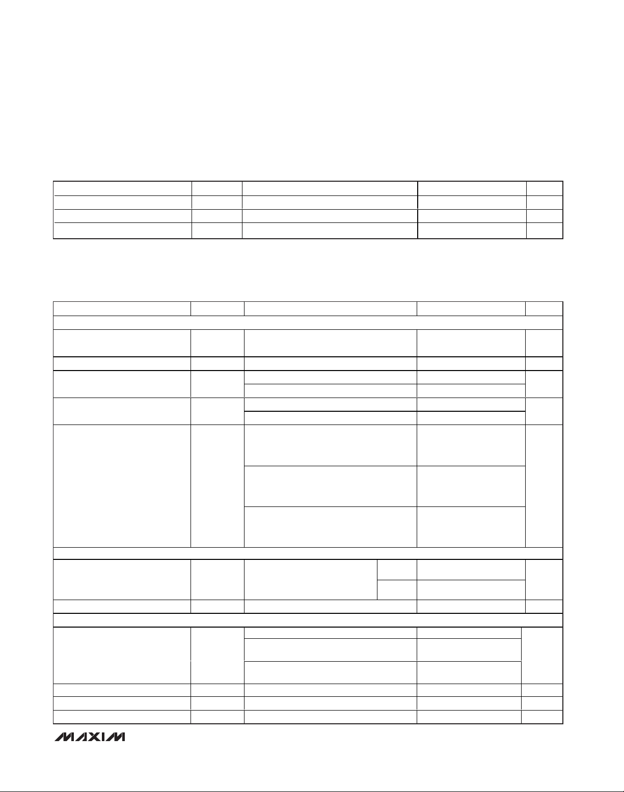
Pulldown Sink Current AGC 0- 2, E N ABLE , T/R, D ATA ( V
Output-Low Voltage V
Output-High Voltage V
OL
OH
I
= 500µA 0.15 V
SINK
I
SOURCE
= 500µA V
PARAMETER SYMBOL CONDITIONS MIN TYP MAX UNITS
GENERAL CHARACTERISTICS
Frequency Range
Maximum Input Level P
Transmit Efficiency 100% Duty
Cycle
Transmit Efficiency 50% Duty
Cycle
RFIN
fRF = 315MHz (Note 6) 32
f
RF
fRF = 315MHz (Note 6) 24
f
RF
ENABLE or T/R transition low to high,
transmitter frequency settled to within
50kHz of the desired carrier
= 434MHz (Note 6) 30
= 434MHz (Note 6) 22
= 5.5V ) 20 µA
H V I N
- 0.26 V
H V IN
315/345/
433.92
0 dBm
200
MHz
%
%
ENABLE or T/R transition low to high,
Power-On Time t
ON
transmitter frequency settled to within 5kHz
350
µs
of the desired carrier
ENABLE transition low to high, or T/R
transition high to low, receiver startup time
250
(Note 5)
RECEIVER
Sensitivity
0.2% BER, 4kbps Manchester
data rate, 280kHz IF BW,
average RF power
315MHz -114
dBm
434MHz -113
Image Rejection 46 dB
POWER AMPLIFIER
TA = +25°C (Note 4) 4.6 10.0 15.5
Output Power P
OUT
TA = +125°C, V
= +2.1V (Note 2)
V
HVIN
TA = -40°C, V
V
= +3.6V (Note 4)
HVIN
PAVDD
PAVDD
= V
= V
AVDD
AVDD
= V
= V
DVDD
DVDD
=
3.9 6.7
=
13.1 15.8
dBm
Modulation Depth 82 dB
Maximum Carrier Harmonics With output-matching network -40 dBc
Reference Spur -50 dBc
MAX7030
Low-Cost, 315MHz, 345MHz, and 433.92MHz
ASK Transceiver with Fractional-N PLL
4 _______________________________________________________________________________________
AC ELECTRICAL CHARACTERISTICS (continued)
(
Typical Application Circuit
, 50Ω system impedance, V
PAVDD
= V
AVDD
= V
DVDD
= V
HVIN
= +2.1V to +3.6V, fRF= 315MHz, 345MHz, or
433.92MHz, T
A
= -40°C to +125°C, unless otherwise noted. Typical values are at V
PAVDD
= V
AVDD
= V
DVDD
= V
HVIN
= +2.7V,
T
A
= +25°C, unless otherwise noted.) (Note 1)
PHASE-LOCKED LOOP
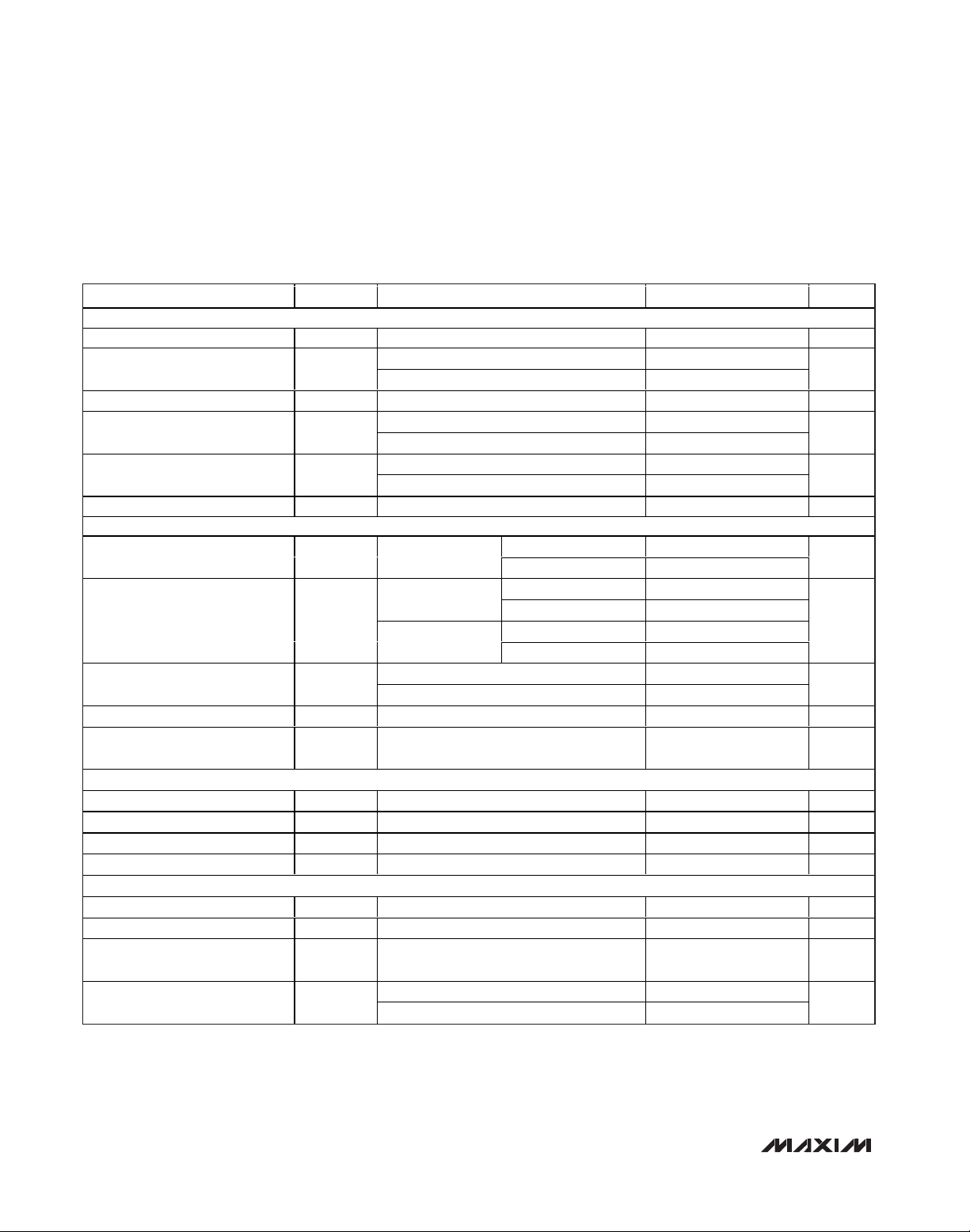
Transmit VCO Gain K
Transmit PLL Phase Noise
Receive VCO Gain 340 MHz/V
Receive PLL Phase Noise
Loop Bandwidth
Reference Frequency Input Level 0.5 V
LOW-NOISE AMPLIFIER/MIXER (Note 8)
LNA Input Impedance Z
Voltage-Conversion Gain
Input-Referred, 3rd-Order
Intercept Point
Mixer-Output Impedance 330 Ω
LO Signal Feedthrough to
Antenna
RSSI
Input Impedance 330 Ω
Operating Frequency f
3dB Bandwidth 10 MHz
Gain 15 mV/dB
ANALOG BASEBAND
Maximum Data-Filter Bandwidth 50 kHz
Maximum Data-Slicer Bandwidth 100 kHz
Maximum Peak-Detector
Bandwidth
Maximum Data Rate
PARAMETER SYMBOL CONDITIONS MIN TYP MAX UNITS
VCO
10kHz offset, 200kHz loop BW -68
1MHz offset, 200kHz loop BW -98
10kHz offset, 500kHz loop BW -80
1MHz offset, 500kHz loop BW -90
Transmit PLL 200
Receive PLL 500
INLNA
IIP3
IF
Normalized to 50Ω
High-gain state
Low-gain state
High-gain state -42
Low-gain state -6
Manchester coded 33
Nonreturn to zero (NRZ) 66
fRF = 315MHz 1 - j4.7
f
RF
fRF = 315MHz 50
f
RF
fRF = 315MHz 13
f
RF
= 434MHz 1- j3.3
= 434MHz 45
= 434MHz 9
340 MHz/V
-100 dBm
10.7 MHz
50 kHz
dBc/Hz
dBc/Hz
kHz
P-P
dB
dBm
kbps
MAX7030
Low-Cost, 315MHz, 345MHz, and 433.92MHz
ASK Transceiver with Fractional-N PLL
_______________________________________________________________________________________ 5
AC ELECTRICAL CHARACTERISTICS (continued)
(
Typical Application Circuit
, 50Ω system impedance, V
PAVDD
= V
AVDD
= V
DVDD
= V
HVIN
= +2.1V to +3.6V, fRF= 315MHz, 345MHz, or
433.92MHz, T
A
= -40°C to +125°C, unless otherwise noted. Typical values are at V
PAVDD
= V
AVDD
= V
DVDD
= V
HVIN
= +2.7V,
T
A
= +25°C, unless otherwise noted.) (Note 1)
Note 1: Supply current, output power, and efficiency are greatly dependent on board layout and PAOUT match.
Note 2: 100% tested at T
A
= +125°C. Guaranteed by design and characterization overtemperature.
Note 3: 50% duty cycle at 10kHz ASK data (Manchester coded).
Note 4: Guaranteed by design and characterization. Not production tested.
Note 5: Time for final signal detection; does not include baseband filter settling.
Note 6: Efficiency = P
OUT
/(VDDx IDD).
Note 7: Dependent on PCB trace capacitance.
Note 8: Input impedance is measured at the LNAIN pin. Note that the impedance at 315MHz includes the 12nH inductive degenera-
tion from the LNA source to ground. The impedance at 434MHz includes a 10nH inductive degeneration connected from
the LNA source to ground. The equivalent input circuit is 50Ω in series with ~2.2pF. The voltage conversion is measured
with the LNA input-matching inductor, the degeneration inductor, and the LNA/mixer tank in place, and does not include the
IF filter insertion loss.
Typical Operating Characteristics
(
Typical Application Circuit
, V
PAVDD
= V
AVDD
= V
DVDD
= V
HVIN
= +3.0V, fRF= 433.92MHz, IF BW = 280kHz, 4kbps Manchester encod-
ed, 0.2% BER, T
A
= +25°C, unless otherwise noted.)
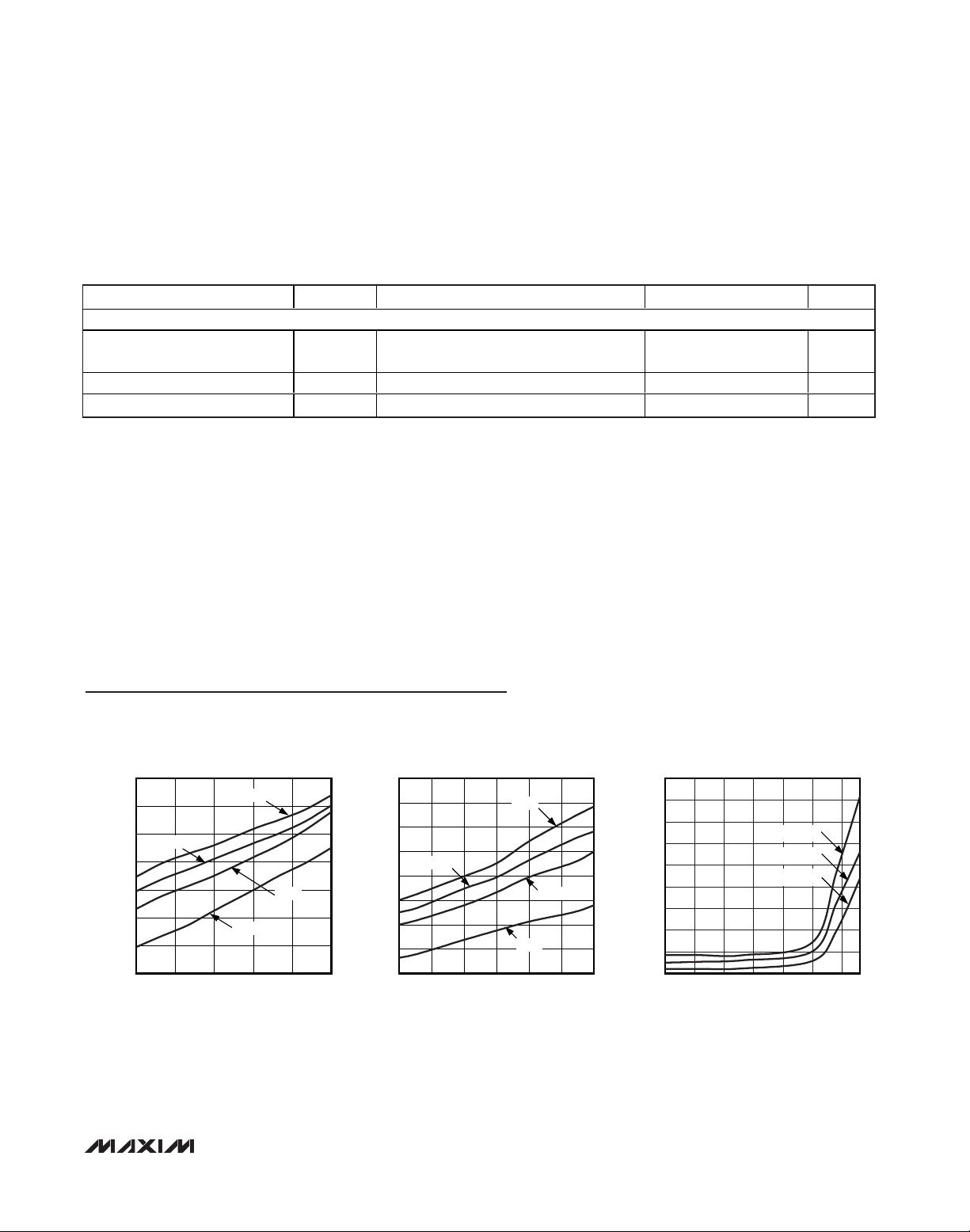
SUPPLY CURRENT vs. SUPPLY VOLTAGE
MAX7030 toc01
SUPPLY VOLTAGE (V)
SUPPLY CURRENT (mA)
3.33.02.72.4
5.8
6.0
6.2
6.4
6.6
6.8
7.0
5.6
2.1 3.6
+85°C
+125°C
+25°C
-40°C
SUPPLY CURRENT vs. RF FREQUENCY
MAX7030 toc02
RF FREQUENCY (MHz)
SUPPLY CURRENT (mA)
425400325 350 375
6.1
6.2
6.3
6.4
6.5
6.6
6.7
6.8
6.0
300 450
+85°C
+125°C
+25°C
-40°C
DEEP-SLEEP CURRENT vs. TEMPERATURE
MAX7030 toc03
TEMPERATURE (°C)
DEEP-SLEEP CURRENT (µA)
1108535 60-10-15
2
4
6
8
10
12
14
16
18
0
-40
VCC = +3.6V
VCC = +3.0V
VCC = +2.1V
RECEIVER
PARAMETER SYMBOL CONDITIONS MIN TYP MAX UNITS
CRYSTAL OSCILLATOR
Crystal Frequency f
Frequency Pulling by V
Crystal Load Capacitance (Note 7) 4.5 pF
XTAL
DD
(f
RF
-10.7)
/24
MHz
2 ppm/V
MAX7030
Low-Cost, 315MHz, 345MHz, and 433.92MHz
ASK Transceiver with Fractional-N PLL
6 _______________________________________________________________________________________
Typical Operating Characteristics (continued)
(
Typical Application Circuit
, V
PAVDD
= V
AVDD
= V
DVDD
= V
HVIN
= +3.0V, fRF= 433.92MHz, IF BW = 280kHz, 4kbps Manchester encod-
ed, 0.2% BER, T
A
= +25°C, unless otherwise noted.)
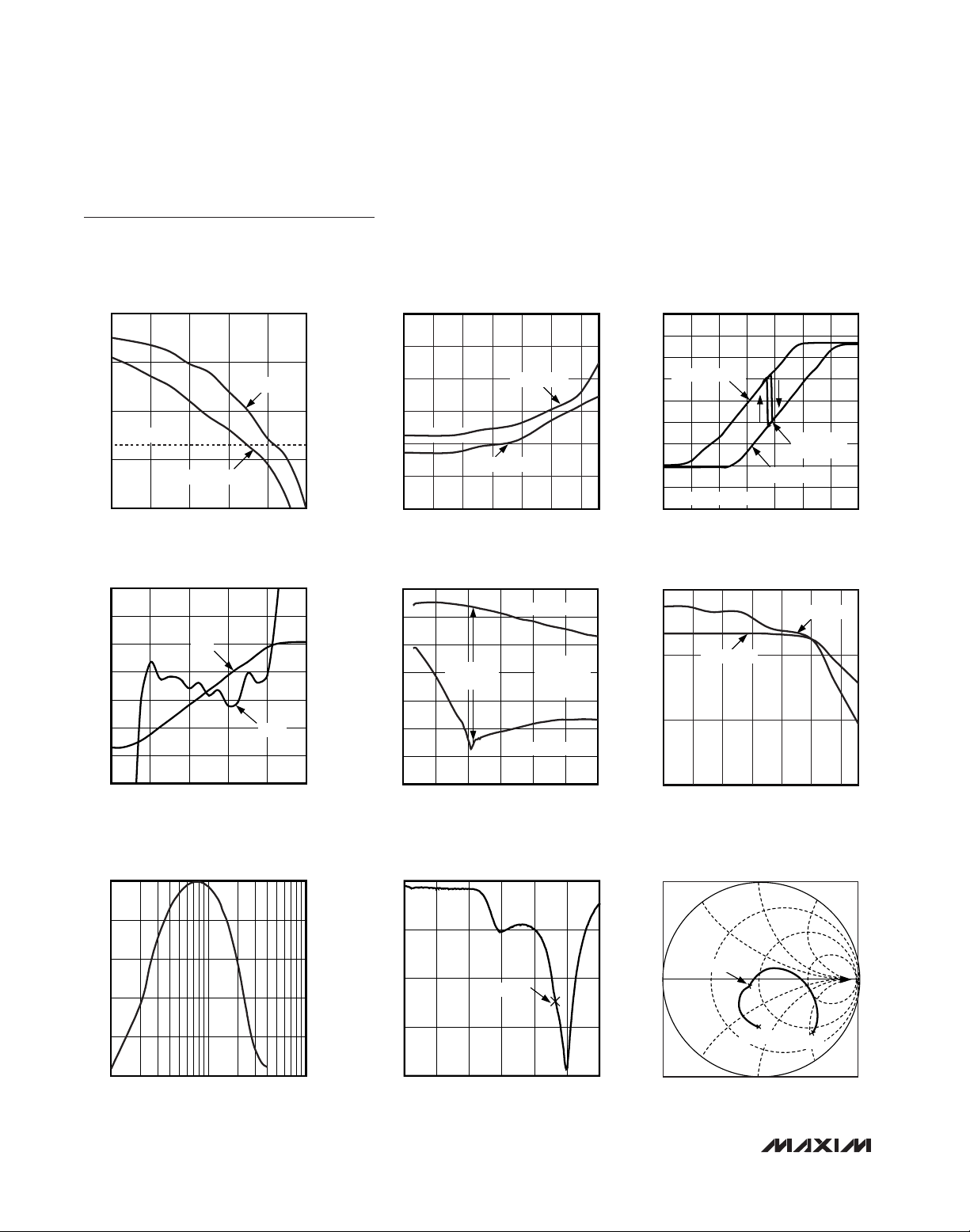
RECEIVER
BIT-ERROR RATE
vs. AVERAGE INPUT POWER
100
10
1
BIT-ERROR RATE (%)
0.2% BER
0.1
fRF = 315MHz
0.01
-121 -111
AVERAGE INPUT POWER (dBm)
fRF = 434MHz
-113-115-117-119
MAX7030 toc04
-102
-105
-108
-111
SENSITIVITY (dBm)
-114
-117
-120
SENSITIVITY vs. TEMPERATURE
fRF = 434MHz
fRF = 315MHz
-40
TEMPERATURE (°C)
1.8
RSSI vs. RF INPUT POWER
1.6
MAX7030 toc05
1.4
HIGH-GAIN MODE
1.2
1.0
RSSI (V)
0.8
0.6
0.4
0.2
AGC HYSTERESIS: 3dB
0
11085603510-15
-130 10
LOW-GAIN MODE
RF INPUT POWER (dBm)
AGC SWITCH
POINT
-10-30-70 -50-90-110
MAX7030 toc06
RSSI AND DELTA vs. IF INPUT POWER
2.1
1.8
1.5
1.2
RSSI (V)
0.9
0.6
0.3
0
-90 10
RSSI
IF INPUT POWER (dBm)
NORMALIZED IF GAIN vs. IF FREQUENCY
0
-4
-8
-12
NORMALIZED IF GAIN (dB)
-16
MAX7030 toc07
DELTA
-10-30-50-70
3.5
2.5
1.5
0.5
-0.5
-1.5
-2.5
-3.5
MAX7030 toc10
50
40
30
20
DELTA (%)
10
SYSTEM GAIN (dBm)
0
-10
-20
030
0
-6
-12
S11 (dB)
-18
SYSTEM GAIN vs. IF FREQUENCY
UPPER SIDEBAND
48dB IMAGE
REJECTION
IF FREQUENCY (MHz)
FROM RFIN
TO MIXOUT
= 434MHz
f
RF
LOWER SIDEBAND
252015105
S11 vs. RF FREQUENCY
433.92MHz
48
MAX7030 toc08
46
44
IMAGE REJECTION (dB)
42
-40
MAX7030 toc11
IMAGE REJECTION vs. TEMPERATURE
fRF = 433MHz
fRF = 315MHz
11085603510-15
TEMPERATURE (°C)
S11 SMITH PLOT OF R
433MHz
400MHz
FIN
500MHz
MAX7030 toc09
MAX7030 toc12
-20
1100
10
IF FREQUENCY (MHz)
-24
200 500
RF FREQUENCY (MHz)
450400350300250
 Loading...