

Page 1
General Description
The MAX6966/MAX6967 serial-interfaced peripherals
provide microprocessors with 10 I/O ports rated to 7V.
Each port can be individually configured as either:
• A 20mA constant-current LED driver (static or pulsewidth modulated (PWM)).
• A 10mA constant-current LED driver (static or PWM).
• An open-drain logic output.
• An overvoltage-protected Schmitt logic input.
Analog and switching LED intensity control is built in:
• Individual 8-bit PWM control per output.
• Individual 1-bit analog control (half/full) per output.
• Global 3-bit analog control applies to all LED outputs.
PWM timing of the 10 port outputs may be optionally
staggered, consecutively phased in 45° increments.
This spreads the PWM load currents over time in eight
steps, helping to even out the power-supply current
and reduce the RMS current.
The MAX6966/MAX6967 can be configured to awake
from shutdown on receipt of a minimum 3ms pulse on
the CS input. This hardware-wakeup feature allows a
power-management controller or similar ASIC to enable
the MAX6966/MAX6967 with preconfigured LED intensity settings.
Shutdown can be programmed to wait up to 4s, fade
down the sink currents to zero for a period of 1/16s to
4s, and then shut down. A similar ramp-up from shutdown can be programmed for 1/16s to 4s.
The MAX6966/MAX6967 support hot insertion. All port
pins remain high impedance in power-down (V+ = 0V)
with up to 8V asserted on them.
The DOUT/OSC pin can be configured as either the
serial interface data output or optional PWM clock
input. The MAX6966 powers up defaulting as DOUT
output. The MAX6967 defaults as OSC input.
For a similar part without the constant-current controls,
refer to the MAX7317 data sheet.
Applications
LCD Backlights RGB LED Drivers
Keypad Backlights Portable Equipment
LED Status Indication Cellular Phones
Features
♦ High-Speed 26MHz SPI-™/QSPI-™/MICROWIRE™-
Compatible Serial Interface
♦ 2.25V to 3.6V Operation
♦ I/O Ports Default to High-Z (LEDs Off) on Power-Up
♦ I/O Port Inputs Are Overvoltage Protected to 7V
♦ I/O Port Outputs Are 7V-Rated Open Drain
♦ I/O Port Outputs Are 10mA or 20mA Constant-
Current Static/PWM LED Drivers, or Open-Drain
Logic Outputs
♦ I/O Ports Support Hot Insertion
♦ Individual 8-Bit PWM Intensity Control for Each LED
♦ Any Output May Use or Not Use PWM Control
♦ Exit Shutdown (Warm Start) with Simple CS Pulse
♦ Auto Ramp-Down into Shutdown
♦ Auto Ramp-Up Out from Shutdown
♦ 0.8µA (typ), 2µA (max) Shutdown Current
♦ Tiny 3mm x 3mm, 0.8mm High Thin QFN Package
♦ -40°C to +125°C Temperature Range
MAX6966/MAX6967
10-Port Constant-Current LED Drivers and I/O
Expanders with PWM Intensity Control
________________________________________________________________ Maxim Integrated Products 1
Ordering Information
19-3487; Rev 2; 4/05
For pricing, delivery, and ordering information, please contact Maxim/Dallas Direct! at
1-888-629-4642, or visit Maxim’s website at www.maxim-ic.com.
EVALUATION KIT
AVAILABLE
PART
TEMP
PINPACKAGE
TOP
PKG
CODE
MAX6966ATE
-40°C to
16 Thin QFN
3mm x 3mm x
0.8mm
T1633-4
MAX6966AEE
-40°C to
16 QSOP — —
MAX6967ATE
-40°C to
16 Thin QFN
3mm x 3mm x
0.8mm
T1633-4
MAX6967AEE
-40°C to
16 QSOP — —
SPI and QSPI are trademarks of Motorola, Inc.
MICROWIRE is a trademark of National Semiconductor Corp.
RANGE
+125°C
+125°C
+125°C
+125°C
MARK
ACF
ACG
Page 2
MAX6966/MAX6967
10-Port Constant-Current LED Drivers and I/O
Expanders with PWM Intensity Control
2 _______________________________________________________________________________________
ABSOLUTE MAXIMUM RATINGS
Stresses beyond those listed under “Absolute Maximum Ratings” may cause permanent damage to the device. These are stress ratings only, and functional
operation of the device at these or any other conditions beyond those indicated in the operational sections of the specifications is not implied. Exposure to
absolute maximum rating conditions for extended periods may affect device reliability.
Voltage (with respect to GND)
V+ .............................................................................-0.3V to +4V
SCLK, DIN, CS, DOUT/OSC.........................-0.3V to (V+ + 0.3V)
P_ .............................................................................-0.3V to +8V
DC Current into P_ .............................................................24mA
DC Current into DOUT/OSC................................................10mA
Total GND Current ............................................................280mA
Continuous Power Dissipation
16-Pin QSOP (derate 8.3mW/°C over T
A
= +70°C) ....667mW
16-Pin QFN (derate 14.7mW/°C over T
A
= +70°C)...1176mW
Operating Temperature Range (T
MIN
to T
MAX
).-40°C to +125°C
Junction Temperature......................................................+150°C
Storage Temperature Range .............................-65°C to +150°C
Lead Temperature (soldering, 10s) .................................+300°C
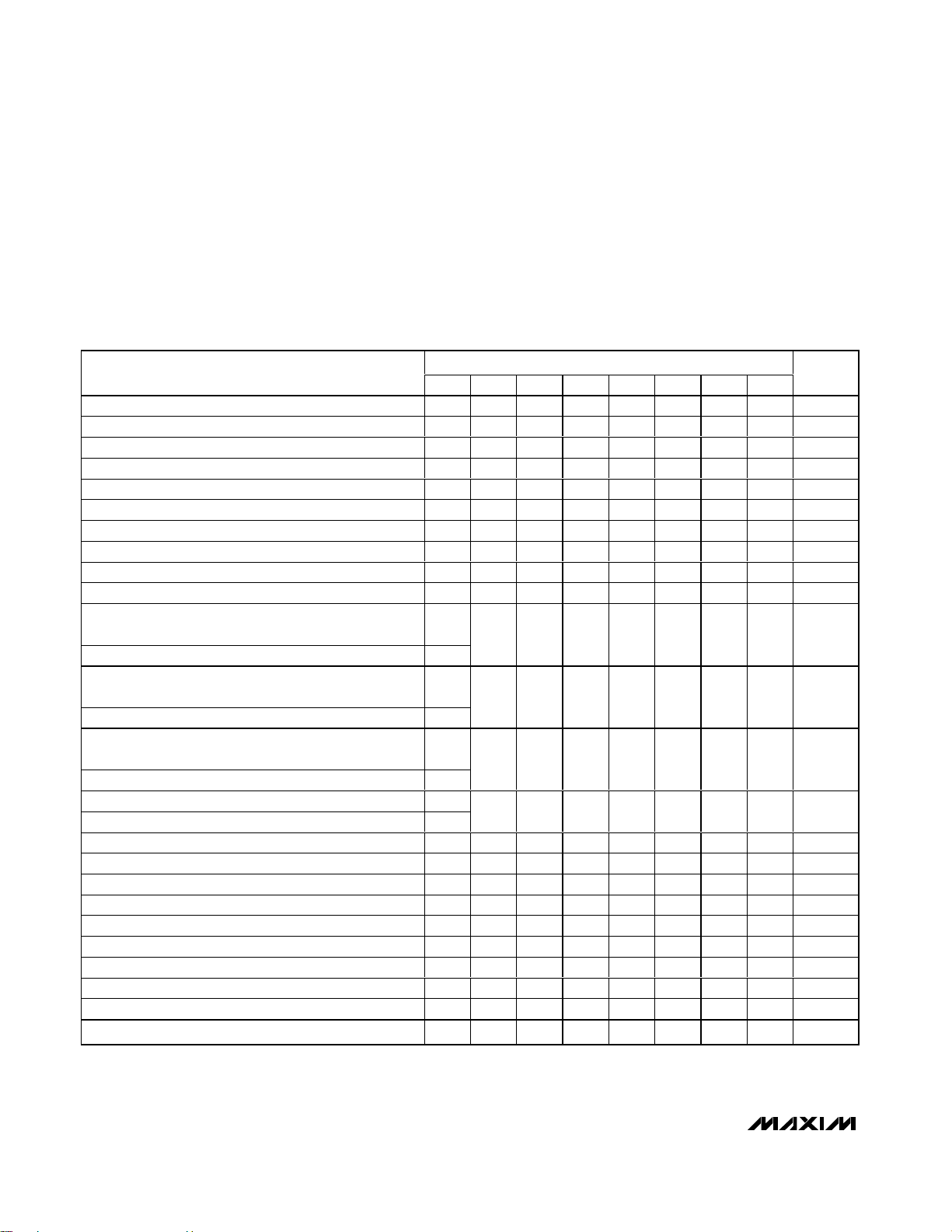
ELECTRICAL CHARACTERISTICS
(Typical Operating Circuit, V+ = 2.25V to 3.6V, TA= T
MIN
to T
MAX
, unless otherwise noted. Typical values are at V+ = 3.3V, TA=
+25°C.) (Note 1)
PARAMETER
SYMBOL
CONDITIONS
MIN
TYP
MAX
UNITS
Operating Supply Voltage V+
V
Output Load External Supply
Voltage P0–P9
V
EXT
7V
TA = +25°C 0.7 1.5
1.7
Standby Current
(Interface Idle, CS Run Disabled,
PWM Disabled, All Ports High
Impedance)
I
STBY
CS at V+; other digital
inputs at V+ or GND
1.9
µA
TA = +25°C
Supply-Current Interface Only
(CS Run Enabled, PWM
Disabled, All Ports High
Impedance)
I
+
f
SCLK
= 26MHz, other
digital inputs at V+ or
µA
TA = +25°C
1.8
1.9
Delta Supply Current per 10mA
Port (Interface Idle, Global
Current Register Set to 0x07, One
Port's Output Register Set to
0x02 and Its Output Current
Register Bit Cleared; All Other
Ports’ Output Registers Set to
0x00, 0x01, or 0xFF)
∆I
+10
Digital inputs at V+ or
GND
2
mA
TA = +25°C 3.2 3.6
3.8
Delta Supply Current per 20mA
Port
( Inter face Id l e, Gl ob al C ur r ent
Reg i ster S et to 0x07, One P or t' s
Outp ut Reg i ster S et to 0x02 and Its
Outp ut C ur r ent Reg i ster Bi t S et; Al l
Other P or ts’ Outp ut Reg i ster s S et to
0x00, 0x01, or 0xFF)
∆I
+20
Digital inputs at V+ or
GND
4.0
mA
2.25 3.60
GND; DOUT unloaded
TA= T
TA= T
TA = T
T
A
TA = T
TA = T
TA = T
TA = T
to +85°C
MIN
to T
MIN
MAX
to +85°C 680
MIN
= T
to T
MIN
MAX
to +85°C
MIN
to T
MIN
to +85°C
MIN
to T
MIN
MAX
MAX
390 620
730
1.58
Page 3
MAX6966/MAX6967
10-Port Constant-Current LED Drivers and I/O
Expanders with PWM Intensity Control
_______________________________________________________________________________________ 3
ELECTRICAL CHARACTERISTICS (continued)
(Typical Operating Circuit, V+ = 2.25V to 3.6V, TA= T
MIN
to T
MAX
, unless otherwise noted. Typical values are at V+ = 3.3V, TA=
+25°C.) (Note 1)
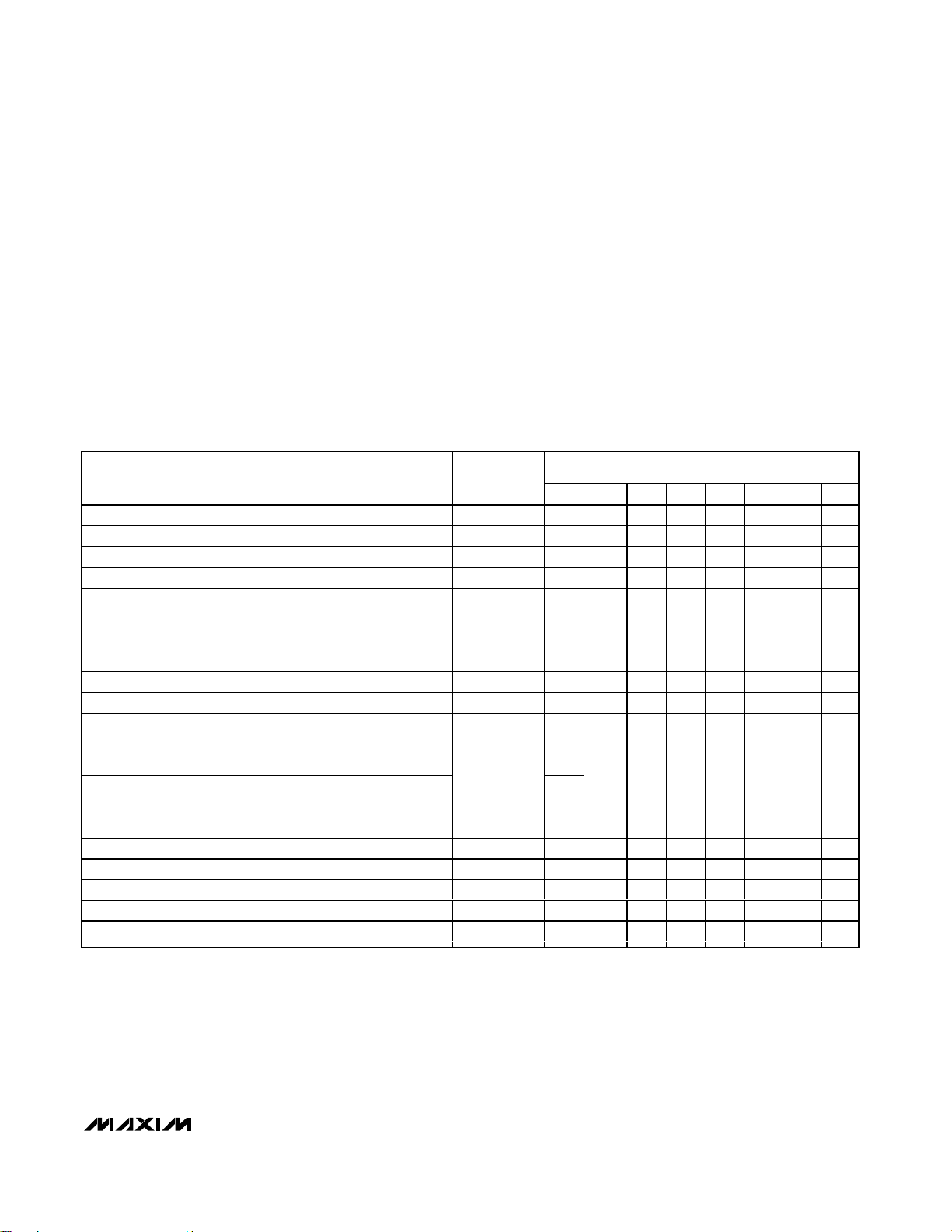
PARAMETER
SYMBOL
CONDITIONS
MIN
TYP
MAX
UNITS
Input High Voltage
(P0–P9, DIN, SCLK, CS, OSC)
V
IH
P0–P9: output register set to 0x01
0.7 x
V+
V
Input Low Voltage
(P0–P9, DIN, SCLK, CS, OSC)
V
IL
P0–P9: output register set to 0x01
0.3 x
V+
V
Input Leakage Current
(P0–P9, DIN, SCLK, CS, OSC)
I
IH
, I
IL
µA
Input Capacitance
(P0–P9, DIN, SCLK, CS, OSC)
(Note 2) 10 pF
20
TA = +25°C
9.5 10
Port Nominal Sink Constant
Current
(P0–P9) (Global Current Register
Set to 0x07)
I
OUT
Output register set to
0x02,
V+ = 3.3V, V
EXT
- V
LED
=
1V to 2.5V (Note 3)
T
A
= T
MIN
to
+85°C
9.1
mA
Port Logic Output Low Voltage
(P0–P9)
V
OLP_
Output register set to 0x00,
I
SINK
= 0.5mA
0.4 V
Port Logic Output Low ShortCircuit Current (P0–P9)
Output register set to 0x00,
V
OLP_
= 5V
20 mA
Port Slew Time From 20% current to 80% current 2 µs
TA = +25°C, V+ = 3.3V, V
EXT
- V
LED
= 1.4V,
I
OUT
= 20mA
±4
Port Sink Constant-Current
Matching
∆I
OUT
TA = +25°C, V+ = 3.3V, V
EXT
- V
LED
= 1.4V,
I
OUT
= 10mA
±2 ±5
%
Output High Voltage
(DOUT)
I
SOURCE
= 6mA
V+ -
V
Output Low Voltage
(DOUT)
I
SINK
= 6mA 0.3 V
-0.2 +0.2
19.3
18.8 21.8
10.8
±1.5
21.1
10.7
11.0
V
OHDOUT
V
OLDOUT
0.3V
Page 4
MAX6966/MAX6967
10-Port Constant-Current LED Drivers and I/O
Expanders with PWM Intensity Control
4 _______________________________________________________________________________________
TIMING CHARACTERISTICS
(Typical Operating Circuit, V+ = 2.25V to 3.6V, TA= T
MIN
to T
MAX
, unless otherwise noted. Typical values are at V+ = 3.3V, TA=
+25°C.) (Note 1)
PARAMETER
SYMBOL
CONDITIONS
MIN
TYP
MAX
UNITS
Internal PWM Clock Frequency f
INT
Hz
External PWM Clock Frequency f
OSC
kHz
SCLK Clock Period t
CP
ns
SCLK Pulse Width High t
CH
19 ns
SCLK Pulse Width Low t
CL
19 ns
CS Fall to SCLK Rise Setup Time
t
CSS
9.5 ns
SCLK Rise to CS Rise Hold Time
t
CSH
0ns
DIN Setup Time t
DS
9.5 ns
DIN Hold Time t
DH
0ns
Output Data Propagation Delay t
DO
21 ns
DOUT Output Rise and Fall
Times
t
FT
C
LOAD
= 20pF 10 ns
Minimum CS Pulse High t
CSW
ns
CS Pulse Low to Not Activate CS
Run
t
CSRUN
CS run enabled
µs
CS Pulse Width to Activate CS
Run
t
CSRUN
CS run enabled 3 ms
Note 1: All parameters tested at TA= +25°C. Specifications over temperature are guaranteed by design.
Note 2: Guaranteed by design.
Note 3: Port current is factory trimmed to meet a median sink current of 20mA and 10mA over all 10 ports. The ∆I
OUT
specification
guarantees current matching between ports.
27000 45000
100
38.4
38.4
640
Page 5
Typical Operating Characteristics
(TA = +25°C, unless otherwise noted.)
MAX6966/MAX6967
10-Port Constant-Current LED Drivers and I/O
Expanders with PWM Intensity Control
_______________________________________________________________________________________ 5
STANDBY CURRENT (I
STBY1
)
vs. TEMPERATURE
MAX6966/67 toc01
TEMPERATURE (°C)
STANDBY CURRENT (µA)
11095-25 -10 5 35 50 6520 80
0.5
0.6
0.7
0.8
0.9
1.0
1.1
1.2
0.4
-40 125
V+ = 3.6V
V+ = 3.3V
V+ = 2.7V
V+ = 2.25V
SUPPLY CURRENT (I+)
vs. TEMPERATURE
MAX6966/67 toc02
TEMPERATURE (°C)
SUPPLY CURRENT (mA)
1109580655035205-10-25
0.1
0.2
0.3
0.4
0.5
0
-40 125
V+ = 3.6V
V+ = 3.3V
V+ = 2.7V
V+ = 2.25V
OUTPUT SINKING CURRENT
vs. V
EXT
- V
LED
AT 10mA
MAX6966/67 toc03
V
EXT
- V
LED
(V)
OUTPUT SINKING CURRENT (mA)
4321
2
4
6
8
10
12
14
0
05
OUTPUT SINKING CURRENT
vs. V
EXT
- V
LED
AT 20mA
MAX6966/67 toc04
V
EXT
- V
LED
(V)
OUTPUT SINKING CURRENT (mA)
4321
4
8
12
16
20
24
0
05
INTERNAL OSCILLATOR FREQUENCY
vs. TEMPERATURE
MAX6966/67 toc05
TEMPERATURE (°C)
FREQUENCY (kHz)
1109565 80-10 5 20 35 50-25
29
31
33
35
37
39
41
43
45
27
-40 125
V+ = 3.6V
V+ = 3.3V
V+ = 2.7V
V+ = 2.25V
SAMPLE PWM WAVEFORMS
2ms
OUTPUT
REGISTER
= 0x03
OUTPUT
REGISTER
= 0x80
OUTPUT
REGISTER
= 0xFE
MAX6966/67 toc06
STAGGER PWM PORT WAVEFORMS
(OUTPUT REGISTERS SET TO 0x80)
2ms
PORT P4
PORT P0
PORT P1
MAX6966/67 toc07
Page 6
MAX6966/MAX6967
Quick-Start Guide
This section describes how to configure a MAX6966 or
MAX6967 on power-up.
Software engineers can use this section as a plain-text
guide to the device’s initialization routine. Hardware
engineers can use this section to get a quick overview
of the device’s capabilities and feature tradeoffs:
1) Before power-up, all 10 I/O ports P0 to P9 are high
impedance. They may be connected to inputs up to
+7V or loads connected to independent rails up to
+7V. The SPI bus inputs (SCLK, CS, DIN) are not
overvoltage protected, and must not be driven from
a voltage higher than V+.
2) After power-up, all 10 I/O ports P0 to P9 remain
high impedance. They may be connected to inputs
up to +7V or loads connected to V+ or independent
rails up to +7V. The ports are not configured as logic
inputs even though the ports are high impedance.
The device is in shutdown mode, and draws minimum supply current regardless of I/O ports connections.
3) Decide whether the DOUT/OSC pin will be used
as SPI data output or PWM clock input, and
choose the MAX6966 or MAX6967 accordingly. If
any ports are used as logic input, or if the application needs read-after-write validation, then
DOUT/OSC needs to be configured as DOUT. Note
that both the MAX6966 and MAX6967 can configure
DOUT/OSC as either DOUT output or OSC clock
input; the only difference is the power-up default.
4) Allocate port functionality for the 10 I/O ports. All
ports have the same features, so allocate ports for
either software convenience or board-routing reasons. Any port can be constant-current LED drivers
(static or PWM), an open-drain logic output, or a
logic input. If fewer than 10 ports are used as constant-current drivers, see the Applications
Information section for details on how to optimize the
PWM phasing to minimize load supply-current modulation.
5) Decide how to implement LED intensity control.
The MAX6966/MAX6967 provide:
• Individual 8-bit PWM control per constant-current
output
• Individual 1-bit analog control (half/full) per
constant-current output
• Global 3-bit analog control, which applies to all
constant-current outputs
10-Port Constant-Current LED Drivers and I/O
Expanders with PWM Intensity Control
6 _______________________________________________________________________________________
Pin Description
PIN
QSOP
NAME FUNCTION
1 15 SCLK
Serial-Clock Input. On SCLK’s rising edge, data shifts into the internal shift register. On SCLK’s
falling edge, data is clocked out of DOUT. SCLK is active only while CS is low.
216 CS
Chip-Select Input. Serial data is loaded into the shift register while CS is low. The most recent 16
bits of data latch on CS’s rising edge.
3–7,
9-13
7-11
P0-P9
I/O Ports. P0 to P9 can be configured as open-drain current-sink outputs rated at 20mA
maximum, or as CMOS-logic inputs, or as open-drain logic outputs. Loads should be connected
to a supply voltage no higher than 7V.
8 6 GND Ground
14 12
Serial-Data Output. The data into DIN is valid at DOUT 15.5 clock cycles later. Use this pin to
daisy-chain several devices or allow data readback. Output is push-pull.
OSC Input. Apply a square-wave CMOS clock up to 100kHz as alternate PWM clock source.
The MAX6966 powers up with DOUT/OSC defaulting as DOUT output.
The MAX6967 powers up with DOUT/OSC defaulting as OSC input.
15 13 DIN
Serial-Data Input. Data from DIN loads into the internal 16-bit shift register on SCLK’s rising
edge.
16 14 V+ Positive Supply Voltage. Bypass V+ to GND with a 0.1µF ceramic capacitor.
— PAD
Exposed
pad
Exposed Pad on Package Underside. Connect to GND.
TQFN
1–5,
DOUT/OSC
Page 7
The tradeoff for LED intensity control is between
depth of current-control resolution, noise constraints,
and software complexity:
• For high LED resolution where each LED needs
individual intensity settings, use the 8-bit PWM
control plus the 1-bit analog control to get 9 bits
of individual LED intensity control.
• For absolute maximum LED resolution where the
LED uses the same intensity settings, use the 8bit PWM control plus the 1-bit analog control,
plus the global 3-bit analog control to get 12 bits
of LED intensity control.
• For lowest noise applications where PWM cannot
be used, 1 bit of individual analog control is
available. If all LEDs use the same intensity settings, the 1-bit analog control plus the global 3bit analog control provide 4 bits of static LED
intensity control.
• If the standard half/full constant-current settings
of 10mA/20mA are not acceptable, then the
global 3-bit analog control can be used to
reduce the currents for all the constant-current
outputs.
6) Take care with PC board layout. The MAX6966/
MAX6967 are switching moderate currents in PWM
applications, so the MAX6966/MAX6967 and the
load supplies need careful decoupling to minimize
conducted noise. Also, the serial interface is fast, so
simple overshoot-damping terminations may be
required if the tracks are long.
Detailed Description
The MAX6966/MAX6967 are general-purpose input/output (GPIO) peripherals that provide 10 I/O ports, P0 to
P9, controlled through a high-speed SPI-compatible
serial interface. The 10 I/O ports can be used as logic
inputs, open-drain logic outputs, or constant-current
sinks in any combination. Ports withstand 7V independent of the MAX6966’s or MAX6967’s supply voltage
whether used as logic inputs, logic outputs, or constant-current sinks.
Ports configured as constant-current outputs can be set
to sink either a constant current of either 10mA or 20mA.
The static port current may be PWM with a duty cycle
ranging from 3/256 to 254/256 to reduce the average
current, or remain static.
Ports configured as open-drain logic outputs have a
relatively weak sink capability, which should still be
adequate for normal logic-level outputs. Open-drain
logic outputs typically require external pullup resistors
to the appropriate positive supply to provide the logichigh reference. The weak drive means that the shortcircuit current is low enough that inadvertently driving
an LED from a port configured as a logic output is
unlikely to damage the LED.
The MAX6966/MAX6967 are rated for all 10 outputs to
carry their maximum 20mA loads at the same time. The
port configuration options are shown in Table 1.
MAX6966/MAX6967
10-Port Constant-Current LED Drivers and I/O
Expanders with PWM Intensity Control
_______________________________________________________________________________________ 7
PORT TYPE
OUTPUT
REGISTER
CODE
BEHAVIOR OUT OF
SHUTDOWN (CONFIGURATION
REGISTER BIT D0 = 1)
BEHAVIOR IN SHUTDOWN
(CONFIGURATION REGISTER
BIT D0 = 0)
APPLICATION NOTES
Low-logic
output
0x00 Logic-low output, not constant current
High-logic
output
Logic-high output with external pullup resistor; otherwise, high
impedance
Logic input
0x01
CMOS logic input
Lowest supply current
unaffected by shutdown
Constantcurrent static
sink output
0x02
Static constant-current sink
output
Full constant-current drive
with no PWM noise
Constantcurrent PWM
output
High impedance
Adjustable constant current
LED off 0xFF
Logic-high output with external pullup resistor; otherwise, high
impedance
LED off
Table 1. Port Configuration Options
0x03–0xFE PWM constant-current sink output
Page 8
MAX6966/MAX6967
Figure 1 shows the I/O port structure of the MAX6966/
MAX6967. I/O ports P0 to P9 default to high impedance
on power-up, so LED or other port loads connected
draw no current, and ports used as inputs do not load
their source signals.
Standby Mode and Operating Current
When all the ports are configured as logic inputs or outputs (all output registers set to value 0x00 or 0x01) or
LED off (output register set to value 0xFF), the
MAX6966/MAX6967 operate at their lowest supply current, called standby mode.
When PWM intensity control is used (one or more output registers set to a value between 0x03 and 0xFE),
the operating current increases because the internal
PWM circuitry is running.
The operating current also increases whenever a port
that is set is active low as a constant-current output
(output register set to a value between 0x02 and 0xFE),
even if a load is not applied to the port. This current
increase is due to an internal current mirror being
enabled for that port output to provide the accurate
constant-current sink. There is a gated mirror for each
output, and each mirror is only enabled when required.
When PWM is used, a current mirror is only turned on
for the output’s on-time. This means that operating current varies as constant-current outputs are turned on
and off through the serial interface, as well as by the
PWM intensity control.
Shutdown Mode
In shutdown mode, all ports configured as constant-current outputs (output register set to a value between 0x02
and 0xFE) are switched off, and these outputs go high
impedance as if their registers were set to value 0xFF.
Ports configured as logic inputs or outputs (output registers set to value 0x00 or 0x01) are unaffected (Table 1).
This means that any ports used for GPIOs are still fully
operational in shutdown mode, and port inputs can be
read and output ports can be toggled at any time using
the serial interface. The MAX6966/MAX6967 can therefore be used for a mix of logic inputs, logic outputs, and
PWM LED drivers, and only the LED drivers are turned
off automatically in shutdown.
The MAX6966/MAX6967 are put into shutdown mode
by clearing the run bit (bit D0) in the configuration register (Table 4). Shutdown is exited by setting the run bit
through the serial interface, or by using the CS run
option discussed below. The MAX6966/MAX6967 can
be configured and controlled in the normal way through
the serial interface in shutdown mode. All registers are
accessible in shutdown mode, and no register is
changed by shutdown mode. When shutdown mode is
exited, ports configured as constant-current outputs at
that time start instantly with their current PWM values.
10-Port Constant-Current LED Drivers and I/O
Expanders with PWM Intensity Control
8 _______________________________________________________________________________________
Figure 1. Simplified Schematic of I/O Ports
I/O PORT
8-BIT LATCH
OUTPUT PORT
REGISTER
1-BIT LATCH
TO/FROM
SERIAL
INTERFACE
OUTPUT CURRENT
REGISTER
3-BIT LATCH
GLOBAL CURRENT
REGISTER
PORT COMMAND
READ I/O
POSITION A: 0x00 - 0x01
POSITION B: 0x02 - 0xFF
CLOSE SWITCH: 0x02-0xFE
MSB
AB
PWM
GENERATOR
4-BIT DAC
ENABLE
SET
CURRENT
ENABLE = 0x00
N
Page 9

If a port is changed from static logic low (0x00) or static
logic high (0x01) to a constant-current value
(0x02–0xFE) in shutdown mode, then that output is
automatically turned off (logic high, or high impedance)
like any other constant-current outputs that are disabled in shutdown. When shutdown mode is exited, the
new constant-current output starts just like any other
constant-current outputs.
If a port is changed from a constant-current value
(0x02–0xFE) to static logic low (0x00) or static logic
high (0x01) in shutdown mode, then that output is
instantly set to that value as a GPIO output. When shutdown mode is exited, the new GPIO output is unaffected just like any other GPIO outputs.
CS Run Option
The MAX6966/MAX6967 can be configured so that a
relatively long pulse on the CS input brings the driver
out of shutdown, as an alternative method to the normal
method of writing the configuration register through the
serial interface. When the CS run option is enabled, a
minimum pulse on CS sets the run bit in the configuration register, bringing the driver out of shutdown and
activating any preconfigured ramp-up. Also, the SPI
interface must be operated at a minimum data rate to
ensure that a normal active-low CS pulse during a 16bit regular data transmission is not mistaken for a CS
run command.
The CS run timing uses the PWM clock, which is either
the internal nominal 32kHz oscillator or a user-provided
clock fed into the dual-use DOUT/OSC pin (see the PWM
Clock section for details on configuring the PWM clock).
The minimum pulse on CS to trigger CS run and bring
the driver out of shutdown is 256 to 257 periods of the
PWM clock. For the internal oscillator, this time is 257 /
27000 = 9.52ms. For the external PWM clock, this time
is 257 / OSC and has a shortest possible time of
2.57ms when OSC is set to the maximum allowed
100kHz frequency.
The maximum pulse on CS to ensure that CS run is not
triggered (when enabled) is 255 periods of the PWM
clock. For the internal oscillator, this time is 255 / 45000
= 5.66ms. Since a transmission on the serial interface
comprises 16 clocks with CS low, a minimum 2.83kHz
SCLK frequency ensures that CS run is not triggered.
For the external PWM clock, this time is 255 / OSC and
has a shortest time of 2.55ms when OSC is set to the
maximum allowed frequency of 100kHz.
The SPI serial interface circuitry is independent of the
CS run circuitry. Activity on SCLK and DIN is ignored
by the CS run circuitry. A slow SPI transmission to the
MAX6966/MAX6967 can therefore be used as both a
valid data transmission (read or write), and as a means
for exiting shutdown. The CS run action (i.e., setting the
run bit in the configuration register) occurs before any
coincident data transmission is processed. This means
that a slow transmission containing a write command to
the configuration register clearing the run bit would
work, since the write command is implemented internally after the CS run action that sets the run bit.
The "slow transmission" cut-off data rate is expected to
be lower than the SPI interface speed in the majority of
applications. If this is not the case, the CS run option
can still be used. Consider the situation when the
MAX6966/MAX6967 have been put into shutdown with
the CS run option enabled. The application uses the
MAX6966/MAX6967 with some ports configured as
logic inputs or outputs, which need to be accessed in
shutdown. The SPI interface speed is slow, so any
transmission brings the MAX6966/MAX6967 out of shutdown. So, how are the I/O ports accessed in shutdown? The solution is to write the configuration register
disabling CS run (bit D1 = 0) and invoking shutdown
(bit D0 = 0) as the first command. Now any other registers can be accessed while the MAX6966/MAX6967
remain in shutdown. Finally, write the configuration register reenabling CS run (bit D1 = 1) and invoking shutdown (bit D0 = 0) to restore the original status.
MAX6966/MAX6967
10-Port Constant-Current LED Drivers and I/O
Expanders with PWM Intensity Control
_______________________________________________________________________________________ 9
Page 10
MAX6966/MAX6967
Register Structure
The MAX6966/MAX6967 contain 16 internal registers,
addressed as 0x00–0x09, and 0x10–0x15, which configure and control the peripheral (Table 2). Two
addresses, 0x0E and 0x0F, do not store data but return
the port input status when read. Four virtual addresses,
0x0A–0x0D allow more than one register to be written
with the same data to simplify software. The no-op
address, 0x20, causes no action when written or read,
and is used as a dummy register when accessing one
MAX6966/MAX6967 out of multiple cascaded devices.
10-Port Constant-Current LED Drivers and I/O
Expanders with PWM Intensity Control
10 ______________________________________________________________________________________
COMMAND ADDRESS
REGISTER
HEX
CODE
Port P0 output level or PWM
00000000x00
Port P1 output level or PWM
00000010x01
Port P2 output level or PWM
00000100x02
Port P3 output level or PWM
00000110x03
Port P4 output level or PWM
00001000x04
Port P5 output level or PWM
00001010x05
Port P6 output level or PWM
00001100x06
Port P7 output level or PWM
00001110x07
Port P8 output level or PWM
00010000x08
Port P9 output level or PWM
00010010x09
Write ports P0 through P9 with same output level or
PWM
0
Read port P0 output level or PWM 1
00010100x0A
Write ports P0 through P3 with same output level or
PWM
0
Read port P0 output level or PWM 1
00010110x0B
Write ports P4 through P7 with same output level or
PWM
0
Read port P4 output level or PWM 1
00011000x0C
Write ports P8 or P9 with same output level or PWM 0
Read port P8 output level or PWM 1
00011010x0D
Read ports P7 through P0 inputs 1 00011100x0E
Read ports P9 and P8 inputs 1 00011110x0F
Configuration
00100000x10
Ramp-down
00100010x11
Ramp-up
00100100x12
Output current ISET70
00100110x13
Output current ISET98
00101000x14
Global current
00101010x15
No-op
01000000x20
Factory reserved; do not write to this register
11111010x7D
Table 2. Register Address Map
D15 D14 D13 D12 D11 D10 D9 D8
R/W
R/W
R/W
R/W
R/W
R/W
R/W
R/W
R/W
R/W
R/W
R/W
R/W
R/W
R/W
R/W
R/W
R/W
Page 11
MAX6966/MAX6967
10-Port Constant-Current LED Drivers and I/O
Expanders with PWM Intensity Control
______________________________________________________________________________________ 11
REGISTER DATA
REGISTER POWER-UP CONDITION
ADDRESS
D0
Port P0 output level or PWM
Port 0 high impedance 0x00
1
1
Port P1 output level or PWM
Port 1 high impedance 0x01
1
1
Port P2 output level or PWM
Port 2 high impedance 0x02
1
1
Port P3 output level or PWM
Port 3 high impedance 0x03
1
1
Port P4 output level or PWM
Port 4 high impedance 0x04
1
1
Port P5 output level or PWM
Port 5 high impedance 0x05
1
1
Port P6 output level or PWM
Port 6 high impedance 0x06
1
1
Port P7 output level or PWM
Port 7 high impedance 0x07
1
1
Port P8 output level or PWM
Port 8 high impedance 0x08
1
1
Port P9 output level or PWM
Port 9 high impedance 0x09
1
1
Configuration (MAX6966
only)
Shutdown mode,
CS run disabled,
Configuration (MAX6967
only)
Shutdown mode,
CS run disabled,
DOUT/OSC is OSC input
0x10
0
0
Ramp-down Fade disabled 0x11
0
0
Ramp-up — 0x12
0
0
Output current ISET70
0x13
0
0
Output current ISET98
0x14
0
0
Global current Full current 0x15
0
1
Table 3. Initial Power-Up Register Status
Initial Power-Up
On power-up, all control registers are reset (Table 3).
Power-up status sets I/O ports P0 to P9 high impedance, and puts the device into shutdown mode. This
means that any LED (or other) loads are effectively
turned off, and the MAX6966/MAX6967 start in its lowest power condition.
PWM Clock
An internal 32kHz oscillator generates PWM timing. If
all output ports are set to static levels, the internal oscil-
lator and PWM logic are disabled automatically, and
the MAX6966/MAX6967 operating current is lowest.
The internal 32kHz oscillator can be replaced by a user
clock up to 100kHz if a precise or synchronized PWM
frequency source is desired. The clock is fed into the
dual-use DOUT/OSC pin, which is switched between a
port output and a clock input using the OSC bit in the
configuration register (Table 4).
CODE (HEX)
D7 D6 D5 D4 D3 D2 D1
1
1
1
1
1
1
1
1
1
1
11111
11111
11111
11111
11111
11111
11111
11111
11111
11111
DOUT/OSC is DOUT output
I
= 10mA for ports P7–P0
PEAK
I
= 10mA for ports P9, P8
PEAK
0
00000
1
0
0
0
0
0
00000
00000
00000
00000
00011
Page 12
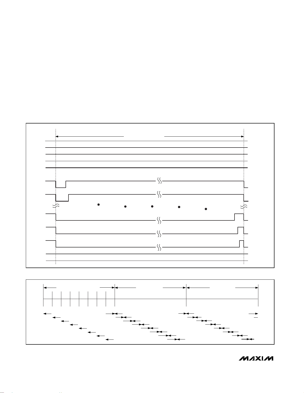
PWM Timing and Phasing
A PWM period comprises 256 cycles of the nominal
32kHz PWM clock (Figure 2). Ports can be set individually to a PWM duty between 3/256 and 254/256.
PWM timing can be configured one of two ways by the
setting of the stagger bit in the configuration register
(Table 4). When the stagger bit is clear, all outputs using
PWM switch at the same time use the timing shown in
Figure 2. All outputs therefore draw load current at exact-
ly the same time for the same PWM setting. This means
that if, for example, all outputs are set to 128/256 duty
cycle, the current draw would be zero (all loads off) for
half the time and full (all loads on) for the other half.
When the stagger bit is set, the PWM timing of the 10 port
outputs is staggered by 32 counts of the 256-count PWM
period (i.e., 1/8), distributing the port output switching
points across the PWM period (Figure 3). The staggering
reduces the di/dt output-switching transient on the supply,
and also reduces the peak/mean current requirement.
MAX6966/MAX6967
10-Port Constant-Current LED Drivers and I/O
Expanders with PWM Intensity Control
12 ______________________________________________________________________________________
HIGH-Z
LOW
HIGH-Z
LOW
HIGH-Z
LOW
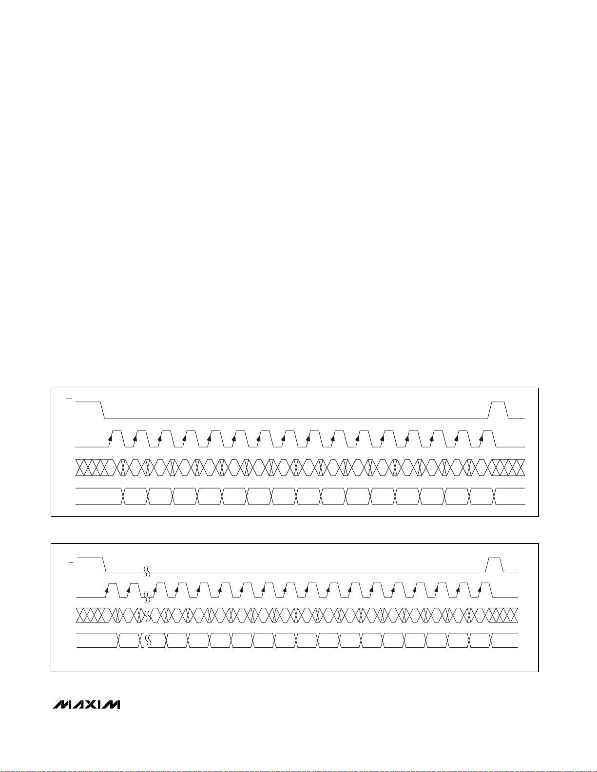
OUTPUT LOW 254/256 DUTY CONSTANT CURRENT WITH INPUT BUFFER DISABLED (PWM LED DRIVE)
HIGH-Z
LOW
0xFF
HIGH-Z
LOW
HIGH-Z
LOW
OUTPUT LOW 253/256 DUTY CONSTANT CURRENT WITH INPUT BUFFER DISABLED (PWM LED DRIVE)
OUTPUT STATIC-HIGH LOGIC DRIVE WITH INPUT BUFFER ENABLED (GPI)
OUTPUT STATIC-LOW LOGIC DRIVE WITH INPUT BUFFER ENABLED (GPI)
OUTPUT STATIC-LOW CONSTANT CURRENT WITH INPUT BUFFER DISABLED (STATIC LED DRIVE ON)
0xFD
0xFE
0x02
0x00
0x01
OUTPUT STATIC HIGH IMPEDANCE WITH INPUT BUFFER DISABLED (STATIC LED DRIVE OFF)
HIGH-Z
LOW
OUTPUT LOW 3/256 DUTY CONSTANT CURRENT WITH INPUT BUFFER DISABLED (PWM LED DRIVE)
0x03
HIGH-Z
LOW
OUTPUT LOW 252/256 DUTY CONSTANT CURRENT WITH INPUT BUFFER DISABLED (PWM LED DRIVE)
0xFC
REGISTER
VALUE
OUTPUT
7.8125ms NOMINAL PWM PERIOD
HIGH-Z
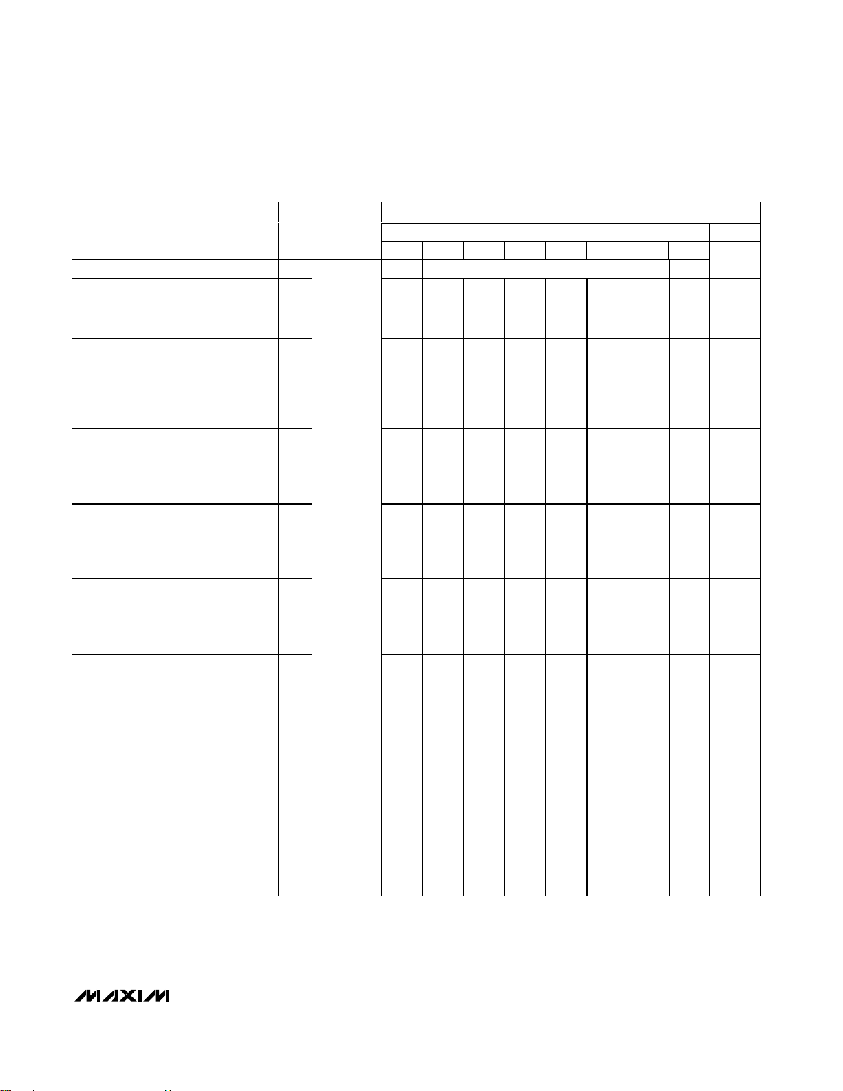
LOW
OUTPUT LOW 4/256 DUTY CONSTANT CURRENT WITH INPUT BUFFER DISABLED (PWM LED DRIVE)
0x04
Figure 2. Static and PWM Constant-Current Waveforms
7.8125ms NOMINAL PWM PERIOD NEXT PWM PERIOD NEXT PWM PERIOD
0 32 64 96 128 160 192 224 256
OUTPUTS P0, O8 IN-PHASE PWM PERIOD
OUTPUT P1, O9 STAGGERED PWM PERIOD
OUTPUT P3 STAGGERED PWM PERIOD
OUTPUT P4 STAGGERED PWM PERIOD
OUTPUT P5 STAGGERED PWM PERIOD
OUTPUT P6 STAGGERED PWM PERIOD
OUTPUT P7 STAGGERED PWM PERIOD
OUTPUTS P0, O8 IN-PHASE PWM PERIOD
OUTPUT P1, O9 STAGGERED PWM PERIOD
OUTPUT P3 STAGGERED PWM PERIOD
OUTPUT P4 STAGGERED PWM PERIOD
OUTPUT P5 STAGGERED PWM PERIOD
OUTPUT P6 STAGGERED PWM PERIOD
OUTPUT P7 STAGGERED PWM PERIOD
OUTPUTS P0, O8 IN-PHASE PWM PERIOD
OUTPUT P1, O9 STAGGERED PWM PERIOD
OUTPUT P2 STAGGERED PWM PERIOD OUTPUT P2 STAGGERED PWM PERIOD
Figure 3. Staggered PWM Waveform
Page 13
MAX6966/MAX6967
10-Port Constant-Current LED Drivers and I/O
Expanders with PWM Intensity Control
______________________________________________________________________________________ 13
REGISTER DATA
REGISTER
R/W
ADDRESS
CODE
(HEX)
D5 D4 D3 D2 D1 D0
CONFIGURATION
DOUT
PWM
Hold-
off
Fade-
off
Ramp-
up
enable/
Sh u t d o w n /
r u n
Write device configuration
Ramp-
up
Read-back device configuration
Hold-
off
Fade-
off
Ramp-
up
Run
Shutdown mode (CS run disabled)
Put or keep device in shutdown,
disable CS run
X
XXXX0 0
Shutdown mode (CS run enabled)
Put or keep device in shutdown,
enable CS run
0x10
X
XXXX1 0
Run mode
(device is currently in run mode)
X
X0*0
*
XX 1
R u n ( e x it sh u t d o w n ) wit h o u t ra m p - u p
(device is currently in shutdown);
bring device out of shutdown
instantly, ignoring fade register setting
X
X0*0
*
0X 1
Run (exit shutdown) with ramp-up
(device is currently in shutdown);
bring device out of shutdown using
fade register ramp-up setting
X
X0*0
*
1X 1
0
*
1
*
1
*
0
*
Run (abort shutdown sequence)
(device is currently in hold-off/fade-off
sequence to shutdown);
bring device out of shutdown
instantly, ignoring fade register setting
X
X
1
*
1
*
1X 1
Status: shutdown mode
X
00 0
0
Status: in fade-off sequence to
shutdown mode
X
01 0
0
Status: in hold-off sequence to
shutdown mode
X
10 0
0
Status: run mode
X
00 0
1
Status: in ramp-up sequence to run
mode
X
00 1
1
PWM outputs are in phase
X
0XXXX X
PWM outputs stagger phase
X
1XXXX X
DOUT/OSC is DOUT output,
PWM clock source is internal oscillator
0
XXXXX X
DOUT/OSC is OSC input,
PWM clock source is OSC
1
XXXXX X
Table 4. Configuration Register
*Current read status of this bit.
0
1
0
0
0
0
0
D7 D6
/OSC
OSC X Stagger
X
stagger
X
X
X
X
X
status
status
status
enable
status
CS run
CS run
0
1
1
1
1
1
X
X
X
X
X
X Stagger
X Stagger
X Stagger
X Stagger
X Stagger
X
X
X
X
CS run
CS run
CS run
CS run
CS run
Page 14

MAX6966/MAX6967
10-Port Constant-Current LED Drivers and I/O
Expanders with PWM Intensity Control
14 ______________________________________________________________________________________
REGISTER DATA
REGISTER
ADDRESS
CODE
(HEX)
D7 D6 D5 D4 D3 D2 D1 D0
Read input ports P7–P0
1 0x0E
Port P0
Read input ports P9–P8
1 0x0F 000000
Port P8
Table 5. Input Ports Register
The stagger bit is ideally set or cleared when the
MAX6966/MAX6967 are in shutdown. If not, there may be
a perceived transient flicker in any PWM-controlled LEDs
because the fundamental PWM timing is being changed.
Configuration Register
The configuration register is used to select PWM phasing between outputs, test fade status, enable hardware
startup from shutdown, and select shutdown or run
mode (Table 4).
GPIO Port Direction Configuration
The 10 I/O ports P0 through P9 can be configured to
any combination of logic inputs, logic outputs, and constant-current outputs. Configure any port as a logic
input by setting its output register to 0x01, which sets
the port output high impedance (Table 6).
Input Ports Registers
Reading an input port register returns the logic levels at
the I/O port pins for ports that have been configured as a
logic input (Table 5). A port is configured as a logic input
by writing 0x01 to the port’s output register (Table 5). An
input ports register returns logic 0 in the appropriate bit
position for a port not configured as a logic input.
The input ports registers are read only. A write to an
input ports register is ignored.
Output Registers and
PWM Intensity Control
The MAX6966/MAX6967 use one 8-bit register to control
each output port (Table 6). Each port may be configured
as a logic input, open-drain logic output, or constant-current sink with programmable current and PWM duty
cycle. Ports withstand 7V independent of the MAX6966’s
or MAX6967’s supply voltage, whether used as logic
inputs, logic outputs, or constant-current sinks.
Ports configured as constant-current outputs sink a constant current set by the output current registers (Table 7)
and the global current registers (Table 8). This current
may be PWM with a duty cycle ranging from 3/256 to
254/256 to reduce the average current, or remain static.
The 10 registers 0x00 through 0x09 control an I/O port
each (Table 6). Five pseudo-register addresses, 0x0B
through 0x0F, allow groups of outputs to be set to the
same value with a single command by writing the same
data to multiple output registers.
PWM timing for LED intensity control is generated using
either the internal 32kHz oscillator, or an external clock
on DOUT/OSC. The PWM clock source is selected by
configuration register bit D7 (Table 4). The MAX6966
powers up configured to use the internal 32kHz oscillator by default. The MAX6967 powers up configured to
use the external clock source by default.
R/W
Port P7 Port P6 Port P5 Port P4 Port P3 Port P2 Port P1
Port P9
Page 15
MAX6966/MAX6967
10-Port Constant-Current LED Drivers and I/O
Expanders with PWM Intensity Control
______________________________________________________________________________________ 15
REGISTER DATA
BINARY
HEX
REGISTER
ADDRESS
CODE
(HEX)
PORT P0 LEVEL OR PWM
OUTPUT P0 LEVEL AND PWM
Port P0 is static-low logic-level logic
port with logic input buffer enabled;
reading this port returns 0. Still active
in shutdown.
00000000
0x00
Port P0 is static-high logic-level logic
port (high impedance without external
pullup) or logic input with logic input
buffer enabled; reading this port
returns 0 or 1, depending on external
conditions. Still active in shutdown.
00000001
0x01
Port P0 is static-low constant-current
sink (PWM disabled). Logic input
buffer is disabled; reading this port
always returns 0. High impedance in
shutdown.
00000010
0x02
Port P0 duty cycle is 3/256 current
sink. GPI logic input buffer is
disabled; reading this port always
returns 0. High impedance in
shutdown.
00000011
0x03
Port P0 duty cycle is 4/256 current
sink. GPI logic input buffer is
disabled; reading this port always
returns 0. High impedance in
shutdown.
00000100
0x04
—
—
—— —
Port P0 duty cycle is 253/256 current
sink. GPI logic input buffer is
disabled; reading this port always
returns 0. High impedance in
shutdown.
11111101
0xFD
Port P0 duty cycle is 254/256 current
sink. GPI logic input buffer is
disabled; reading this port always
returns 0. High impedance in
shutdown.
11111110
0xFE
Port P0 is static high impedance
(PWM disabled). GPI logic input
buffer is disabled; reading this port
always returns 0. High impedance in
shutdown.
0x00
11111111
0xFF
Table 6. Output Registers Format
R/W
X MSB
X
X
X
X
X
X————
X
X
X
D7 D6 D5 D4 D3 D2 D1 D0
—
LSB
Page 16

MAX6966/MAX6967
10-Port Constant-Current LED Drivers and I/O
Expanders with PWM Intensity Control
16 ______________________________________________________________________________________
REGISTER DATA
BINARY
HEX
REGISTER
R/W
ADDRESS
CODE
(HEX)
OUTPUT P0 LEVEL AND PWM
Port P1 level or PWM
0x01
Port P1 level or PWM
Port P2 level or PWM
0x02
Port P2 level or PWM
Port P3 level or PWM
0x03
Port P3 level or PWM
Port P4 level or PWM
0x04
Port P4 level or PWM
Port P5 level or PWM
0x05
Port P5 level or PWM
Port P6 level or PWM
0x06
Port P6 level or PWM
Port P7 level or PWM
0x07
Port P7 level or PWM
Port P8 level or PWM
0x08
Port P8 level or PWM
Port P9 level or PWM
0x09
Port P9 level or PWM
Writes ports P0 through P9 with
same level or PWM
Ports P0 through P9 level or PWM
Reads port P0 level or PWM
0x0A
Port P0 level or PWM
Writes ports P0 through P3 with
same level or PWM
Ports P0 through P3 level or PWM
Reads port P0 level or PWM
0x0B
Port P0 level or PWM
Writes ports P4 through P7 with
same level or PWM
Ports P4 through P7 level or PWM
Reads port P4 level or PWM
0x0C
Port P4 level or PWM
Write ports P8 and P9 with same
level or PWM
Ports P8, P9 level, or PWM
Reads port P8 level or PWM
0x0D
Port P8 level or PWM
0x00
to
0xFF
Table 6. Output Registers Format (continued)
D7 D6 D5 D4 D3 D2 D1 D0
MSB
LSB
X
X
X
X
X
X
X
X
X
0 MSB
1
0 MSB
1
0 MSB
1
0 MSB
1
MSB
MSB
MSB
MSB
MSB
MSB
MSB
MSB
MSB
MSB
MSB
MSB
MSB
LSB
LSB
LSB
LSB
LSB
LSB
LSB
LSB
LSB
LSB
LSB
LSB
LSB
LSB
LSB
LSB
LSB
Page 17

MAX6966/MAX6967
10-Port Constant-Current LED Drivers and I/O
Expanders with PWM Intensity Control
______________________________________________________________________________________ 17
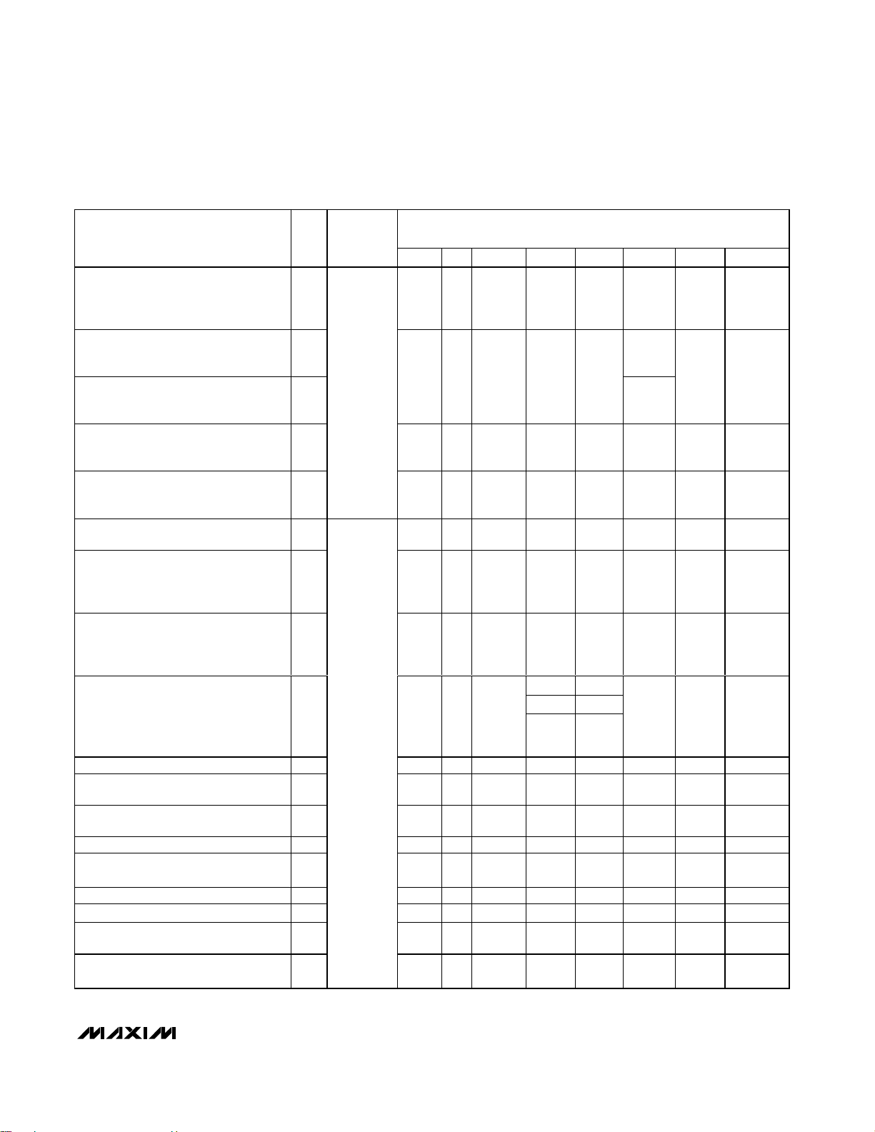
Output Current Registers
Each output port’s individual constant-current sink can
be set to be either half or full global current. The individual currents are set by the output current registers
(Table 7). The global current is set by the global current
register (Table 8).
Each output current can be set individually to best suit
the maximum operating current of an LED load, or even
adjusted on the fly to double the effective intensity control range of each output. When the global current register is set to maximum, the individual current selection
is 10mA (half) or 20mA (full).
REGISTER DATA
REGISTER
ADDRESS
D0
OUTPUT CURRENT IOUT70 X
IOUT7IOUT6IOUT5IOUT4IOUT3IOUT2IOUT
1
IOUT
0
Output P0 is set to half constant current X XXXXXXX0
Output P0 is set to full constant current X XXXXXXX1
Output P1 is set to half constant current X XXXXXX0X
Output P1 is set to full constant current X XXXXXX1X
Output P2 is set to half constant current X XXXXX0XX
Output P2 is set to full constant current X XXXXX1XX
Output P3 is set to half constant current X XXXX0XXX
Output P3 is set to full constant current X XXXX1XXX
Output P4 is set to half constant current X X X X 0 X X X X
Output P4 is set to full constant current X X X X 1 X X X X
Output P5 is set to half constant current X X X 0 X X X X X
Output P5 is set to full constant current X X X 1 X X X X X
Output P6 is set to half constant current X X 0 X X X X X X
Output P6 is set to full constant current X X 1 X X X X X X
Output P7 is set to half constant current X 0 XXXXXXX
Output P7 is set to full constant current X
0x13
1XXXXXXX
0 XXXXXX
IOUT8
OUTPUT CURRENT IOUT98
1 000000
IOUT8
Output P8 is set to half constant current X XXXXXXX0
Output P8 is set to full constant current X XXXXXXX1
Output P9 is set to half constant current X XXXXXX0X
Output P9 is set to full constant current X
0x14
XXXXXX1X
Table 7. Output Current Register Format
R/W
CODE (HEX)
D7 D6 D5 D4 D3 D2 D1
IOUT9
IOUT9
Page 18

Global Current Register
The global current register sets the full (maximum) constant current sunk into an I/O port (Table 8). Each output port’s individual constant-current sink can be set to
be either half or full global current by the output current
registers (Table 7). By default, maximum current is
20mA, so the default half current is 10mA.
Ramp-Up and Ramp-Down Controls
The MAX6966/MAX6967 provide automatic controls
that allow the currents’ outputs to be ramped down into
automatic shutdown (ramp-down), and ramped up
again out of shutdown (ramp-up) without further interaction (Figures 4 and 5). Ramp-down comprises a programmable hold-off delay, which also maintains the
outputs at full current for a time before the programmed
fade-off time, during which the currents’ outputs are
ramped down.
MAX6966/MAX6967
10-Port Constant-Current LED Drivers and I/O
Expanders with PWM Intensity Control
18 ______________________________________________________________________________________
REGISTER DATA
REGISTER
ADDRESS
D0
0 XXXXX
ISET0
GLOBAL CURRENT
1 00000
ISET0
Full current is 2.5mA; half current is
1.25mA
X XXXXX000
Full current is 5mA; half current is 2.5mA
X XXXXX001
Full current is 7.5mA; half current is
3.75mA
X XXXXX010
Full current is 10mA; half current is 5mA X XXXXX01 1
Full current is 12.5mA; half current is
6.25mA
X XXXXX100
Full current is 15mA; half current is 7.5mA
X XXXXX101
Full current is 17.5mA; half current is
8.75mA
X XXXXX110
Full current is 20mA; half current is 10mA
X
0x15
XXXXX111
Table 8. Global Current Register Format
EXIT SHUTDOWN COMMAND
1s 2s1/4s 1/2s
1/8s
1/16s
ZERO TO 4s CURRENT RAMP-UP AFTER CS RUN
4s
Figure 4. Ramp-Up Behavior
ZERO TO 4s HOLD-OFF DELAY BEFORE FADE-OFF
ZERO TO 4s CURRENT FADE-OFF AFTER HOLD-OFF DELAY
1s 2s 4s 1s 2s
1/8s
1/16s
1/8s
1/16s
ZERO TO 8s CURRENT RAMP-DOWN
4s1/4s 1/2s 1/4s 1/2s
Figure 5. Ramp-Down, Hold-Off, and Fade-Off Behavior
R/W
CODE (HEX)
D7 D6 D5 D4 D3 D2 D1
ISET2 ISET1
ISET2 ISET1
Page 19

MAX6966/MAX6967
10-Port Constant-Current LED Drivers and I/O
Expanders with PWM Intensity Control
______________________________________________________________________________________ 19
The ramp-down register sets the hold-off and fade-off
times and allows hold-off and fade-off to be disabled
(zero delay), if desired (Table 9). The ramp-up register
sets the ramp-up time and allows ramp-up to be disabled (zero delay), if desired (Table 10). The configuration register contains 3 status bits that identify whether
the MAX6966/MAX6967 are in hold-off, fade-off, or rampup condition (Table 4). The configuration register also
enables or disables ramp-up. One write to the configuration register can put the MAX6966/MAX6967 into shutdown (using hold-off and fade-off settings in the fade
register) and determine whether CS run is enabled for
restart, and whether ramp-up is to be used for restart.
REGISTER DATA
REGISTER
ADDRESS
CODE
(HEX)
D0
Write ramp-down 0
Read ramp-down 1
Hold-off Fade-off
Fade-off time (f
PWM
= 32768Hz)
Instant going into shutdown after hold-off delay X
0
1/16s ramp-down from full current before shutdown after
hold-off delay
X
1
1/8s ramp-down from full current before shutdown after
hold-off delay
X
0
1/4s ramp-down from full current before shutdown after
hold-off delay
X
1
1/2s ramp-down from full current before shutdown after
hold-off delay
X
0
1s ramp-down from full current before shutdown after
hold-off delay
X
1
2s ramp-down from full current before shutdown after
hold-off delay
X
0
4s ramp-down from full current before shutdown after
hold-off delay
X
1
Hold-off time (f
PWM
= 32768Hz)
Zero hold-off delay before fade-off going into shutdown X
X
1/16s hold-off delay before fade-off going into shutdown X
X
1/8s hold-off delay before fade-off going into shutdown X
X
1/4s hold-off delay before fade-off going into shutdown X
X
1/2s hold-off delay before fade-off going into shutdown X
X
1s hold-off delay before fade-off going into shutdown X
X
2s hold-off delay before fade-off going into shutdown X
X
4s hold-off delay before fade-off going into shutdown X
0x11
X
Table 9. Ramp-Down Register Format
R/W
D7 D6 D5 D4 D3 D2 D1
XX
00
XXXXX00
XXXXX00
XXXXX01
XXXXX01
XXXXX10
XXXXX10
XXXXX11
XXXXX11
XX000XX
XX001XX
XX010XX
XX011XX
XX100XX
XX101XX
XX110XX
XX111XX
Page 20

MAX6966/MAX6967
10-Port Constant-Current LED Drivers and I/O
Expanders with PWM Intensity Control
20 ______________________________________________________________________________________
REGISTER DATA
REGISTER
ADDRESS
CODE
(HEX)
D0
Write ramp-up 0
Read ramp-up 1
Ramp-up
Ramp-up time (f
PWM
= 32768Hz)
Instant full current coming out from shutdown X
0
1/16s ramp-up to full current coming out from shutdown X
0x12
1
1/8s ramp-up to full current coming out from shutdown X
0
1/4s ramp-up to full current coming out from shutdown X
1
1/2s ramp-up to full current coming out from shutdown X
0
1s ramp-up to full current coming out from shutdown X
1
2s ramp-up to full current coming out from shutdown X
0
4s ramp-up to full current coming out from shutdown X
1
Table 10. Ramp-Up Register Format
Ramp-up and ramp-down use the PWM clock for timing.
If the external oscillator is selected, then this clock
should be provided until the end of the sequence. If the
internal oscillator is selected, it always runs during a
fade sequence, even if none of the ports are using PWM.
The ramp-up and ramp-down circuit operates a 3-bit
DAC. The DAC adjusts the internal current reference
used to set the constant-current outputs in a similar
manner to the global current register (Table 8).
Because it is the master current reference that is
scaled, all output constant-current and PWM settings
are adjusted at the same ratio with respect to each
other. This means that LEDs are always faded at the
same rate even if their different intensity settings are
totally different. Figure 6 shows output fade DAC.
The maximum port output current set by the global current register (Table 8) also sets the point during rampdown that the current starts falling, and the point during
ramp-up that the current stops rising. Figure 7 shows
the ramp waveforms that occur with different global
current register settings.
20mA
15mA
10mA
5mA
0mA
CURRENT
FADE-UP
FULL
CURRENT
7/8
CURRENT
6/8
CURRENT
5/8
CURRENT
4/8
CURRENT
3/8
CURRENT
2/8
CURRENT
1/8
CURRENT
ZERO
CURRENT
17.5mA
12.5mA
7.5mA
2.5mA
PORT CURRENT = HALF
FADE-OFF
PORT CURRENT = FULL
Figure 6. Output Fade DAC (Global Current = 0x07)
20mA
15mA
10mA
5mA
0mA
CURRENT
FULL
CURRENT
7/8
CURRENT
6/8
CURRENT
5/8
CURRENT
4/8
CURRENT
3/8
CURRENT
2/8
CURRENT
1/8
CURRENT
ZERO
CURRENT
17.5mA
12.5mA
7.5mA
2.5mA
FADE-UP
FADE-OFF
GLOBAL CURRENT = 0x07
GLOBAL CURRENT = 0x06
GLOBAL CURRENT = 0x05
GLOBAL CURRENT = 0x04
GLOBAL CURRENT = 0x03
GLOBAL CURRENT = 0x02
GLOBAL CURRENT = 0x01
GLOBAL CURRENT = 0x00
Figure 7. Global Current Modifies Fade Behavior
R/W
D7 D6 D5 D4 D3 D2 D1
XXXXX
00000
XXXXX00
XXXXX00
XXXXX01
XXXXX01
XXXXX10
XXXXX10
XXXXX11
XXXXX11
Page 21

MAX6966/MAX6967
10-Port Constant-Current LED Drivers and I/O
Expanders with PWM Intensity Control
______________________________________________________________________________________ 21
Serial Interface
The MAX6966/MAX6967 communicate through an SPIcompatible 4-wire serial interface. The interface has
three inputs: clock (SCLK), chip select (CS), and data
in (DIN), and one output, data out (DOUT). CS must be
low to clock data into or out of the device, and DIN
must be stable when sampled on the rising edge of
SCLK. DOUT is stable on the rising edge of SCLK.
Note that the SPI protocol expects DOUT to be high
impedance when the MAX6966/MAX6967 are not being
accessed; DOUT on the MAX6966/MAX6967 is never
high impedance. Go to www.maxim-ic.com/an1879 for
ways to convert the MAX6966/MAX6967 to tri-state,
if required.
SCLK and DIN can be used to transmit data to other
peripherals. The MAX6966/MAX6967 ignore all activity
on SCLK and DIN except when CS is low.
Control and Operation Using the 4-Wire
Interface
Controlling the MAX6966/MAX6967 requires sending a
16-bit word. The first byte, D15 through D8, is the command, and the second byte, D7 through D0, is the data
byte (Table 11).
Connecting Multiple MAX6966/MAX6967s
to the 4-Wire Bus
Multiple MAX6966/MAX6967s can be interfaced to a
common SPI bus by connecting DIN inputs together,
connecting SCLK inputs together, and providing an
individual CS per MAX6966/MAX6967 device (Figure
8). This connection works regardless of the configuration of DOUT/OSC, but does not allow the MAX6966/
MAX6967s to be read.
D15
D0
R/W
ADDRESS
DATA
LSB
Table 11. Serial-Data Format
DIN
SCLK
CS3
DIN
SCLK
CS2
DIN
SCLK
MOSI
SCLK
CS1
CS3
CS2
CS1
MAX6966
MAX6967
MAX6966
MAX6967
MAX6966
MAX6967
µC
Figure 8. MAX6966/MAX6967 Multiple CS Connection
D14 D13 D12 D11 D10 D9 D8 D7 D6 D5 D4 D3 D2 D1
MSB
LSB MSB
Page 22

MAX6966/MAX6967
10-Port Constant-Current LED Drivers and I/O
Expanders with PWM Intensity Control
22 ______________________________________________________________________________________
Alternatively, the MAX6966/MAX6967s can be daisychained by connecting the DOUT of one device to the
DIN of the next, and driving SCLK and CS lines in parallel (Figure 9). This connection allows the MAX6966/
MAX6967s to be read. Data at DIN propagates through
the internal shift registers and appears at DOUT 15.5
clock cycles later, clocked out on the falling edge of
SCLK. When sending commands to daisy-chained
MAX6966/MAX6967s, all devices are accessed at the
same time. An access requires (16 x n) clock cycles,
where n is the number of MAX6966/MAX6967s connect-
ed together. For daisy-chaining to work, DOUT/OSC
must be configured as DOUT by clearing configuration
register bit D7 to zero (Table 4). Note that the MAX6966
powers up with DOUT/OSC configured as DOUT output
by default, while the MAX6967 powers up with
DOUT/OSC configured as OSC input by default. The
serial-interface speed (maximum SCLK) is limited to
17.5MHz when multiple devices are daisy-chained due
to the DOUT propagation delay and DIN setup time.
Figure 10 is the timing diagram.
SCLK
SCLK
DIN DOUT DOUT DOUT
DIN DIN
SCLK
MOSI
MISO
SCLK
CS CS CS CS
MAX6966
MAX6967
MAX6966
MAX6967
MAX6966
MAX6967
µC
Figure 9. MAX6966/MAX6967 Daisy-Chain Connection
Figure 10. Timing Diagram
CS
t
CSS
SCLK
t
DS
t
DH
DIN
DOUT
t
CL
t
CH
D1D14D15
t
CSW
t
CSH
D0
D15
t
CP
t
DO
Page 23
MAX6966/MAX6967
10-Port Constant-Current LED Drivers and I/O
Expanders with PWM Intensity Control
______________________________________________________________________________________ 23
The MAX6966/MAX6967 are written to using the following sequence (Figure 11):
1) Take SCLK low.
2) Take CS low. This enables the internal 16-bit shift reg-
ister.
3) Clock 16 bits of data into DIN, D15 first to D0 last,
observing the setup and hold times. Bit D15 is low,
indicating a write command.
4) Take CS high (either while SCLK is still high after
clocking in the last data bit, or after taking SCLK
low).
5) Take SCLK low (if not already low).
If fewer or greater than 16 bits are clocked into the
MAX6966/MAX6967 between taking CS low and taking
CS high again, the MAX6966/MAX6967 store the last 16
bits received, including the previous transmission(s).
The general case is when n bits (where n > 16) are
transmitted to the MAX6966/MAX6967. The last bits
comprising bits {n-15} to {n}, are retained, and are parallel loaded into the 16-bit latch as bits D15 to D0,
respectively (Figure 12).
Reading Device Registers
Any register data within the MAX6966/MAX6967 can be
read by sending a logic high to bit D15. The sequence is:
1) Take SCLK low.
2) Take CS low. This enables the internal 16-bit shift
register.
3) Clock 16 bits of data into DIN, D15 first to D0 last.
D15 is high, indicating a read command and bits
D14 through D8 contain the address of the register
to read. Bits D7 to D0 contain dummy data, which is
discarded.
4) Take CS high (either while SCLK is still high after
clocking in the last data bit, or after taking SCLK
low). Positions D7 through D0 in the shift register are
now loaded with the register data addressed by bits
D15 through D8.
5) Take SCLK low (if not already low).
6) Issue another read or write command, and examine
the bit stream at DOUT; the second 8 bits are the
contents of the register addressed by bits D14
through D8 in step 3).
.
D15
= 0
D14 D13 D12 D11 D10 D9 D8 D7 D6 D5 D4 D3 D2 D1 D0
D15 = 0
CS
SCLK
DIN
DOUT
Figure 11. 16-Bit Write Transmission to the MAX6966/MAX6967
.
N-15
N-31 N-30 N-29 N-28 N-27 N-26 N-25 N-24 N-23 N-22 N-21 N-20 N-19 N-18 N-17 N-16
BIT1BIT
2
N-14 N-13 N-12 N-11 N-10 N-9 N-8 N-7 N-6 N-5 N-4 N-3 N-2 N-1 N
CS
SCLK
DIN
DOUT
Figure 12. Transmission of More than 16 Bits to the MAX6966/MAX6967
Page 24

MAX6966/MAX6967
10-Port Constant-Current LED Drivers and I/O
Expanders with PWM Intensity Control
24 ______________________________________________________________________________________
Applications Information
Hot Insertion
The I/O ports P0–P9 remain high impedance with up to
8V asserted on them when the MAX6966/MAX6967 are
powered down (V+ = 0V). The MAX6966/MAX6967 can
therefore be used in hot-swap applications.
SPI Routing Considerations
The MAX6966/MAX6967s’ SPI interface is guaranteed to
operate at 26Mbps on a 2.5V supply, and on a 3.3V supply typically operate at 35Mbps. This means that transmission-line issues should be considered when the
interface connections are longer than 100mm, particularly with higher supply voltages. Avoid running long adjacent tracks for SCLK, DIN, and CS without interleaving
GND traces; otherwise, the signals may cross-couple,
giving false clock or chip-select transitions. Ringing may
manifest itself as communication issues, often intermittent, typically due to double clocking due to ringing at
the SCLK input. Fit a 1kΩ to 10kΩ parallel termination
resistor to either GND or V+ at the DIN, SCLK, and CS
inputs to damp ringing for moderately long interface
runs. Use line-impedance matching terminations when
making connections between boards.
Differences Between the MAX6966 and
MAX6967
The MAX6966 powers up with DOUT/OSC configured
as DOUT output by default. The MAX6967 powers up
with DOUT/OSC configured as OSC input by default.
Both parts allow the DOUT/OSC pin function to be
changed through the configuration register (Table 4). If
any port is used as a logic input, then configure
DOUT/OSC as DOUT to allow the MAX6966/MAX6967
to be read.
In most applications, the software can be written so that
either MAX6966 or MAX6967 can be fitted, and
DOUT/OSC is configured appropriately on power-up. If
DOUT/OSC is used as OSC, fit a series resistor
between the PWM clock source and DOUT/OSC pin. A
resistor value of 2.2kΩ is recommended as a starting
point, but other values may be more suitable depending on the serial-interface speed and clock-source
drive capability. This limits the loading on the PWM
clock source on power-up when a MAX6966 is fitted,
because DOUT/OSC initializes as an output. If
DOUT/OSC is used as DOUT, remember that a
MAX6967 cannot be read after power-up until
DOUT/OSC has been reconfigured from OSC to DOUT.
Driving LEDs into Brownout
The MAX6966/MAX6967 correctly regulate the constant-current outputs, provided there is a minimum voltage drop across the port output. This port output
voltage is the difference between the load (typically
LED) supply and the load voltage drop (LED forward
voltage). If the LED supply drops so that the minimum
port output voltage is not maintained, the driver output
stages brownout and the load current falls. The minimum port voltage is approximately 0.5V at 10mA sink
current, and approximately 1V at 20mA sink current.
In battery applications, it may be important to operate
the LEDs directly from a battery supply. For example,
the LED supply voltage could be a single rechargeable
Li+ battery with a maximum terminal voltage of 4.2V on
charge, 3.4V to 3.7V most of the time, and down to 3V
when discharged. In this scenario, the LED supply falls
significantly below the brownout point when the battery
is at end-of-life voltage.
Page 25

MAX6966/MAX6967
10-Port Constant-Current LED Drivers and I/O
Expanders with PWM Intensity Control
______________________________________________________________________________________ 25
VLED vs. VLED SUPPLY
VLED SUPPLY (V)
VLED (V)
6.56.05.0 5.53.5 4.0 4.53.0
2.55
2.60
2.65
2.70
2.75
2.80
2.85
2.90
2.95
3.00
3.05
2.50
2.5 7.0 6.56.05.0 5.53.5 4.0 4.53.02.5 7.0
ILED vs. VLED SUPPLY
VLED SUPPLY (V)
ILED (mA)
0
2
4
6
8
10
12
14
16
18
20
Figure 13. LED Brownout
Figure 13 shows the typical current sunk by a LITEON
LTST-C170TBKT 3.0V blue LED as the LED supply voltage is varied from 2.5V to 7V. The LED currents shown
are for ports programmed for 10mA and 20mA constant
current, swept over a 2.5V to 7V LED supply voltage
range. It can be seen that the LED forward voltage falls
with current, allowing the LED current to fall gracefully,
not abruptly, in brownout. In practice, the LED current
drops to 6mA to 7mA at a 3V LED supply voltage,
which is an acceptable performance at end-of-life in
many backlight applications.
Output Level Translation
The open-drain output architecture allows the ports to
level translate the outputs to higher or lower voltages
than the MAX6966/MAX6967 supply. An external pullup
resistor can be used on any output to convert the highimpedance logic-high condition to a positive voltage
level. The resistor can be connected to any voltage up
to 7V. When using a pullup on a constant-current output, select the resistor value to sink no more than a few
hundred µA in logic-low condition. This ensures that the
current sink output saturates close to GND. For interfacing CMOS inputs, a pullup resistor value of 220kΩ is
a good starting point. Use a lower resistance to
improve noise immunity in applications where power
consumption is less critical, or where a faster rise time
is needed for a given capacitive load.
Using Stagger with Fewer Ports
The stagger option, when selected, applies to all ports
configured as constant-current outputs. The 10 ports’
PWM cycles are separated to eight evenly spaced start
positions (Figure 3). This phasing can be optimized if
fewer than 10 ports are used as constant-current outputs by allocating the ports with the most appropriate
start positions. If eight constant-current outputs are
needed, choose P0–P7 because these all have different PWM start positions. If four constant-current outputs
are needed, choose P0, P2, P4, P6 or P1, P3, P5, P7
because the PWM start positions are evenly spaced. In
general, choose the ports that spread the PWM start
positions as evenly as possible. This optimally spreads
out the current demand from the ports’ load supply.
Generating a Shutdown/Run Output
An I/O port can be used to automatically generate a
shutdown/run output from the MAX6966/MAX6967. The
shutdown/run output is active low when the
MAX6966/MAX6967 are in run mode, hold-off, fade-off,
or ramp-up, and go high automatically when the
MAX6966/MAX6967 finally enter shutdown after fadeoff. Program the port’s output register to value 0x00,
which puts the output into static constant-current mode
(Table 6). Program the port’s output current register to
half current (Table 7) to minimize operating current. Fit
a 220kΩ pullup resistor to this port.
Page 26
MAX6966
V+
+3.3V
µC
MOSI
+5V
P0
P1
P2
P3
P4
P5
P6
P7
SCLK
DIN
SCLK
GND
MISO
DOUT
CS
P8
D1 D2 D3
+5V +5V
P9
LOGIC INPUT
CS
Typical Application Circuit
TOP VIEW
16
15
14
13
12
11
10
9
1
2
3
4
5
6
7
8
SCLK
V+
DIN
DOUT/OSC
P9
P8
P7
P6
P5
MAX6966ATE
MAX6967ATE
QSOP
CS
P0
P3
P1
P2
P4
GND
12 11 10 9
P9
P8
P7
5
6
7
8
P4
GND
P6
16
15
14
13
CS
SCLK
V+
1234
P0
P1
P2
P3
DIN
P5
DOUT/OSC
THIN QFN
MAX6966ATE
MAX6967ATE
Pin Configurations
MAX6966/MAX6967
In run mode, the output port goes low, approaching 0V,
as the port’s static constant current saturates trying to
sink a higher current than the 220kΩ pullup resistor
can source.
In shutdown mode, the output goes high impedance
together with any other constant-current outputs. This
output remains low during ramp-up and fade-down
sequences because the current drawn by the 220kΩ
pullup resistor is much smaller than the available output
constant current, even at the lowest fade current step.
Driving Load Currents Higher than 20mA
The MAX6966/MAX6967 can be used to drive loads
needing more than 20mA, like high-current white LEDs,
by paralleling outputs. For example, consider a white
LED that needs to be driven with 70mA. This LED can
be driven using ports P0, P1, P2, and P3 connected in
parallel (shorted together). Three of the ports should be
configured for full current (20mA), and the last port
should be configured for half current (10mA) to meet
the 70mA requirement. The four ports can be controlled
simultaneously with one write access using register
0x0B (Table 6). Note that because the output ports
have current limiting, they do not have to be switched
simultaneously to ensure safe current sharing.
Power-Supply Considerations
The MAX6966/MAX6967 operate with a power-supply
voltage of 2.25V to 3.6V. Bypass the power supply to
GND with a 0.1µF ceramic capacitor as close to the
device as possible. For the TQFN version, connect the
underside exposed pad to GND.
10-Port Constant-Current LED Drivers and I/O
Expanders with PWM Intensity Control
26 ______________________________________________________________________________________
Page 27
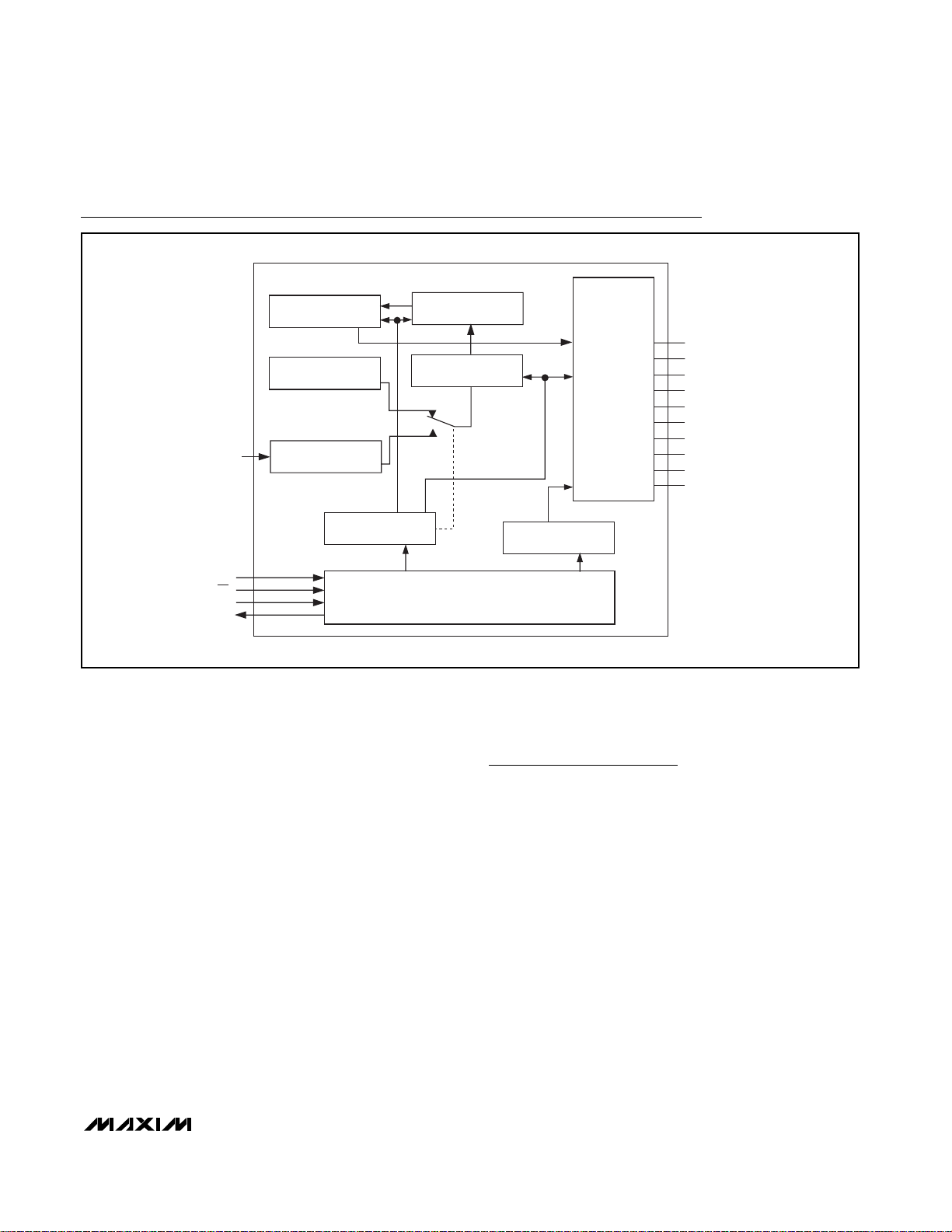
MAX6966/MAX6967
10-Port Constant-Current LED Drivers and I/O
Expanders with PWM Intensity Control
______________________________________________________________________________________ 27
Block Diagram
Chip Information
TRANSISTOR COUNT: 14,865
PROCESS: BiCMOS
CLK
CS
DIN
DOUT
OSC
CURRENT REFERENCE
INTERNAL
OSCILLATOR
EXTERNAL CLOCK INPUT
CONFIGURATION
REGISTER
RAMP-UP/RAMP-DOWN
CONTROLS
PWM CONTROLLER
4-WIRE SERIAL INTERFACE
I/O REGISTER
I/O PORTS
P0
P1
P2
P3
P4
P5
P6
P7
P8
P9
Page 28
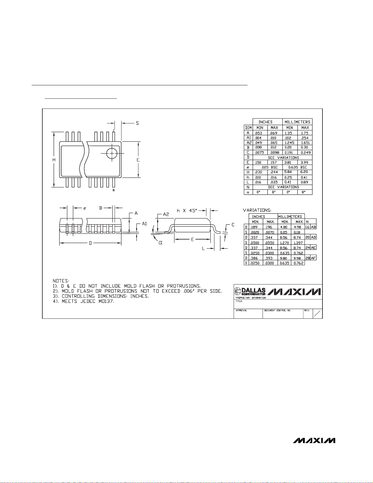
MAX6966/MAX6967
10-Port Constant-Current LED Drivers and I/O
Expanders with PWM Intensity Control
28 ______________________________________________________________________________________
Package Information
(The package drawing(s) in this data sheet may not reflect the most current specifications. For the latest package outline information,
go to www.maxim-ic.com/packages
.)
QSOP.EPS
F
1
1
21-0055
PACKAGE OUTLINE, QSOP .150", .025" LEAD PITCH
Page 29
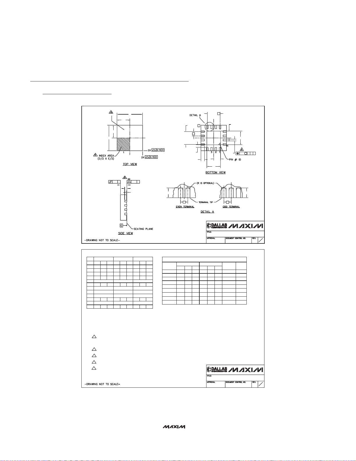
MAX6966/MAX6967
10-Port Constant-Current LED Drivers and I/O
Expanders with PWM Intensity Control
Maxim cannot assume responsibility for use of any circuitry other than circuitry entirely embodied in a Maxim product. No circuit patent licenses are
implied. Maxim reserves the right to change the circuitry and specifications without notice at any time.
Maxim Integrated Products, 120 San Gabriel Drive, Sunnyvale, CA 94086 408-737-7600 ____________________ 29
© 2005 Maxim Integrated Products Printed USA is a registered trademark of Maxim Integrated Products, Inc.
MAX6966/MAX6967MAX6966/MAX6967
Package Information (continued)
(The package drawing(s) in this data sheet may not reflect the most current specifications. For the latest package outline information,
go to www.maxim-ic.com/packages
.)
MARKING
D/2
D
0.10 C 0.08 C
8L 3x3
PKG
REF. MIN.
MIN.
NOM. M
0.70 0.75 0.80
0.25 0.30 0.35
2.90
3.00 3.10
2.90 3.00 3.10
0.65 BSC.
0.35
0.55 0.75
8
2
2
0
0.02
0.20 REF
-
0.25
AX.
0.05
-
A
b
D
E
e
L
ND
NE
A1
A2
k
E/2
AAAA
C
L
12L 3x3
NOM. MAX. NOM.
0.70
0.75
0.80
0.20
0.25
0.30
2.90
3.00
3.10
2.90
3.00
3.10
0.50 BSC.
0.45
0.55
0.65
12N
3
3
0.02
0
0.05
0.20 REF
-
0.25
E
A
A2
A1
MIN. MAX.
0.70
0.20
2.90
2.90
0.30
040.02
-
0.25
16L 3x3
0.75
0.25
3.00
3.00
0.50 BSC.
0.40
16
0.20 REF
(NE - 1) X e
(ND - 1) X e
C
L
L
PKG.
CODES
0.80
0.30
TQ833-1 1.250.25 0.70 0.35 x 45° WEEC1.250.700.25
3.10
T1233-1
3.10
0.50
4
0.05
-
-
3
T1233T1233-4
T1633-2 0.95
T1633F-3
T1633FH-3 0.65 0.80 0.95
T1633-4 0.95
T1633-5 0.95
e
k
L
C
L
e
EXPOSED PAD VARIATIONS
D2
MIN.
NOM.
MAX.
MIN.
1.25
0.95
1.10
0.95
1.25
0.95
1.10
0.95 1.10 0.35 x 45°1.25 WEED-1
1.251.10
0.95
1.25
1.10
0.65
0.95
0.95
0.80
0.65
0.65 0.80
1.10 1.25 0.95 1.10
1.25
1.10
E2
PACKAGE OUTLINE
8, 12, 16L THIN QFN, 3x3x0.8mm
E2
NOM.
1.10
1.100.95
1.10
0.80
1.10
D2/2
D2
b
E2/2
0.10 M C A B
C
L
L
e
21-0136
ID
PIN
0.35 x 45°
0.35 x 45°
0.35 x 45°
0.225 x 45°
0.225 x 45°
0.35 x 45°
0.35 x 45°
JEDEC
WEED-1
WEED-11.25
WEED-2
WEED-2
WEED-2
WEED-2
WEED-20.95
MAX.
1.25
1.25
0.95
0.95
1.25
1.25
12x16L QFN THIN.EPS
1
I
2
NOTES:
1. DIMENSIONING & TOLERANCING CONFORM TO ASME Y14.5M-1994.
2. ALL DIMENSIONS ARE IN MILLIMETERS. ANGLES ARE IN DEGREES.
3. N IS THE TOTAL NUMBER OF TERMINALS.
4. THE TERMINAL #1 IDENTIFIER AND TERMINAL NUMBERING CONVENTION SHALL CONFORM TO
JESD 95-1 SPP-012. DETAILS OF TERMINAL #1 IDENTIFIER ARE OPTIONAL, BUT MUST BE LOCATED
WITHIN THE ZONE INDICATED. THE TERMINAL #1 IDENTIFIER MAY BE EITHER A MOLD OR
MARKED FEATURE.
5. DIMENSION b APPLIES TO METALLIZED TERMINAL AND IS MEASURED BETWEEN 0.20 mm AND 0.25 mm
FROM TERMINAL TIP.
6. ND AND NE REFER TO THE NUMBER OF TERMINALS ON EACH D AND E SIDE RESPECTIVELY.
7. DEPOPULATION IS POSSIBLE IN A SYMMETRICAL FASHION.
8. COPLANARITY APPLIES TO THE EXPOSED HEAT SINK SLUG AS WELL AS THE TERMINALS.
9. DRAWING CONFORMS TO JEDEC MO220 REVISION C.
10. MARKING IS FOR PACKAGE ORIENTATION REFERENCE ONLY.
11. NUMBER OF LEADS SHOWN ARE FOR REFERENCE ONLY.
12. WARPAGE NOT TO EXCEED
0.10mm.
PACKAGE OUTLINE
8, 12, 16L THIN QFN, 3x3x0.8mm
21-0136
2
I
2
 Loading...