

General Description
The MAX6960–MAX6963 are compact cathode-row display drivers that interface microprocessors to 8 x 8 dotmatrix red, green, and yellow (R,G,Y) LED displays
through a high-speed 4-wire serial interface.
The MAX6960–MAX6963 drive two monocolor 8 x 8
matrix displays, or a single RGY 8 x 8 matrix display with
no external components. The driver can also be used
with external pass transistors to control red, green, blue
(RGB) and other displays at higher currents and voltages.
The MAX6960–MAX6963 feature open- and short-circuit
LED detection, and provide both analog and digital tile
segment current calibration to allow 8 x 8 displays from
different batches to be compensated or color matched.
A local 3-wire bus synchronizes multiple interconnected
MAX6960–MAX6963s and automatically allocates memory
map addresses to suit the user’s display-panel
architecture.
The MAX6960–MAX6963s’ 4-wire interface connects multiple drivers, with display memory mapping shared and
allocated among the drivers. A single global write operation can send a command to all MAX6960s in a panel.
The MAX6963 drives monocolor displays with two-step
intensity control. The MAX6962 drives monocolor displays
with two-step or four-step intensity control. The MAX6961
drives monocolor or RGY displays with two-step intensity
control. The MAX6960 drives monocolor or RGY displays
with two-step or four-step intensity control.
Features
♦ 2.7V to 3.6V Operation
♦ High-Speed 20MHz Serial Interface
♦ Trimmed 40mA or 20mA Peak Segment Current
♦ Directly Drives Either Two Monocolor or One RGY
Cathode-Row 8 x 8 Matrix Displays
♦ Analog Digit-by-Digit Segment Current Calibration
♦ Digital Digit-by-Digit Segment Current Calibration
♦ 256-Step Panel Intensity Control (All Drivers)
♦ Four Steps per Color Pixel-Level Intensity Control
♦ Open/Short LED Detection
♦ Burst White to Display Memory Planes
♦ Global Command Access All Devices
♦ Can Control RGB Panels or Higher
Current/Voltage Panels with External Pass
Transistors
♦ Multiple Display Data Planes Ease Animation
♦ Automatic Plane Switching from 63 Planes per
Second to One Plane Every 63s, with Interrupt
♦ Slew-Rate-Limited Segment Drivers for Lower EMI
♦ Driver Switching Timing Can Be Spread Between
Multiple Drivers to Flatten Power-Supply Peak
Demand
♦ Low-Power Shutdown with Full Data Retention
♦ -40°C to +125°C Temperature Range
MAX6960–MAX6963
4-Wire Serially Interfaced
8 x 8 Matrix Graphic LED Drivers
________________________________________________________________ Maxim Integrated Products 1
Ordering Information
19-3696; Rev 3; 6/07
For pricing, delivery, and ordering information, please contact Maxim Direct at 1-888-629-4642,
or visit Maxim’s website at www.maxim-ic.com.
Pin Configurations continued at end of data sheet.
EVALUATION KIT
AVAILABLE
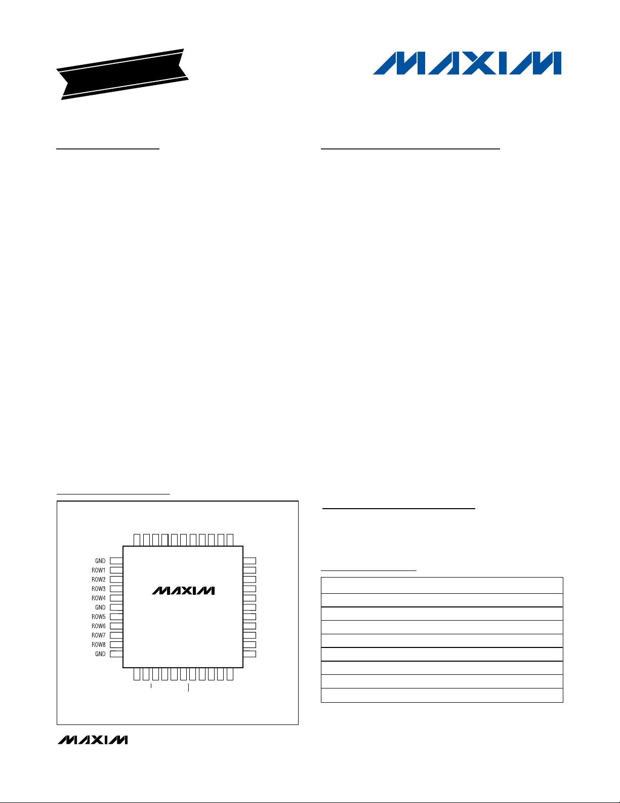
Pin Configurations
Applications
Message Boards Industrial Controls
Gaming Machines Audio/Video Equipment
*EP = Exposed paddle.
TOP VIEW
GND
RISET1
RISET0
ADDCLK
ADDIN
4443424140393837363534
1
2
3
4
5
6
7
8
9
10
11
MAX6960-MAX6963
1213141516171819202122
CS
DIN
OSC
GND
DOUT
MQFP
ADDOUTV+COL16
RST
CLK
COL1
COL15
COL2
COL14
COL3
V+
33
COL13
32
COL12
31
COL11
30
COL10
COL9
29
V+
28
COL8
27
COL7
26
COL6
25
COL5
24
COL4
23
V+
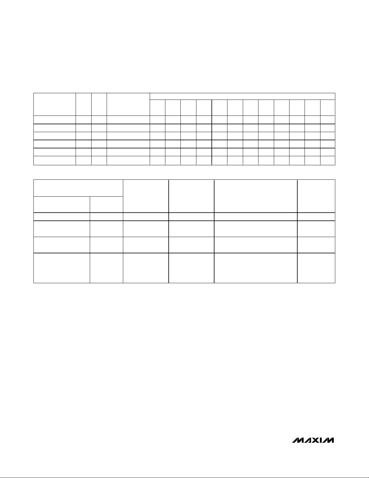
PART TEMP RANGE PIN-PACKAGE PKG CODE
M A X6 9 6 0AM H -40°C to +125°C 44 MQFP —
M AX6960ATH -40°C to +125°C 44 TQFN - E P * T4477- 3
M A X6 9 6 1AM H -40°C to +125°C 44 MQFP —
M AX6961ATH -40°C to +125°C 44 TQFN - E P * T4477-3
M A X6 9 6 2AM H -40°C to +125°C 44 MQFP —
M AX6962ATH -40°C to +125°C 44 TQFN - E P * T4477-3
M A X6 9 6 3AM H -40°C to +125°C 44 MQFP —
M AX6963ATH -40°C to +125°C 44 TQFN - E P * T4477-3
MAX6960–MAX6963
4-Wire Serially Interfaced
8 x 8 Matrix Graphic LED Drivers
2 _______________________________________________________________________________________
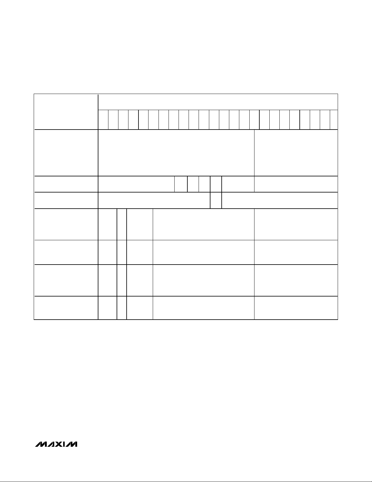
ABSOLUTE MAXIMUM RATINGS
ELECTRICAL CHARACTERISTICS
(V+ = 2.7V to 3.6V, TA= T
MIN
to T
MAX
, typical values at V+ = 3.3V, TA= +25°C, unless otherwise noted.) (Note 1)
Stresses beyond those listed under “Absolute Maximum Ratings” may cause permanent damage to the device. These are stress ratings only, and functional
operation of the device at these or any other conditions beyond those indicated in the operational sections of the specifications is not implied. Exposure to
absolute maximum rating conditions for extended periods may affect device reliability.
(Voltage with respect to GND.)
V+ .............................................................................-0.3V to +4V
All Other Pins................................................-0.3V to (V+ + 0.3V)
ROW1–ROW8 Sink Current ..............................................750mA
COL1–COL16 Source Current ...........................................48mA
Continuous Power Dissipation (T
A
= +70°C)
44-Pin MQFP
(derate 12.7 mW/°C over +70°C)...............................1012mW
44-Pin TQFN
(derate 27mW/°C over +70°C)...................................2162mW
Operating Temperature Range
(T
MIN
to T
MAX
) ..............................................-40°C to +125°C
Junction Temperature......................................................+150°C
Storage Temperature Range .............................-65°C to +150°C
Lead Temperature (soldering, 10s) .................................+300°C
PARAMETER SYMBOL CONDITIONS MIN TYP MAX UNITS
Operating Supply Voltage V+ 2.7 3.6 V
Master Clock Frequency f
Dead-Clock Protection
Frequency
OSC High Time t
OSC Low Time t
Anode Column Source Current
COL1–COL16
Anode Column Source-Current
Temperature Variation
COL1–COL16
Segment Current Slew Rate ΔI
Shutdown mode, all
SHDN
digital inputs at V+
or GND
Intensity set to full,
no display load
connected
OSC
f
OSC
CH
CL
V
= 2.3V, V+ =
LED
3.15V to 3.6V,
current = high
I
SEG
V
= 2.3V, V+ =
LED
2.7V to 3.6V, current
= low
V
= 2.3V, V+ = 3.15V to 3.6V,
LED
I
TC
current = high
V
= 2.2V, V+ = 2.7V to 3.3V,
LED
current = low
/ΔtTA = +25°C 30 mA/µs
SEG
TA = +25°C 250 375
TA = T
T
A
= T
MIN
MIN
to +85°C 500Shutdown Supply Current I
to T
MAX
600
TA = +25°C 7.5 9
TA = T
T
A
= T
MIN
MIN
to +85°C 10Operating Supply Current I+
to T
MAX
11
1.0 8.5 MHz
50 90.5 200 kHz
40 ns
40 ns
TA = +25°C 38 40 42
TA = T
T
A
to +85°C 37 43
MIN
= T
MIN
to T
MAX
37 44
TA = +25°C 19 20 21
TA = T
T
A
to +85°C 18.5 21.5
MIN
= T
MIN
to T
MAX
18.5 22.0
200
200
µA
mA
mA
ppm/°C
MAX6960–MAX6963
4-Wire Serially Interfaced
8 x 8 Matrix Graphic LED Drivers
_______________________________________________________________________________________ 3
ELECTRICAL CHARACTERISTICS (continued)
(V+ = 2.7V to 3.6V, TA= T
MIN
to T
MAX
, typical values at V+ = 3.3V, TA= +25°C, unless otherwise noted.) (Note 1)
Note 1: All parameters are tested at TA= +25°C. Specifications over temperature are guaranteed by design.
PARAMETER SYMBOL CONDITIONS MIN TYP MAX UNITS
LOGIC INPUTS AND OUTPUTS
Input Leakage Current
DIN, CLK, CS, OSC, ADDIN,
ADDCLK, RST
Logic-High Input Voltage
DIN, CLK, CS, OSC, ADDIN,
ADDCLK, RST
Logic-Low Input Voltage
DIN, CLK, CS, OSC, ADDIN,
ADDCLK, RST
DOUT Output Rise and Fall Times t
DOUT Output High Voltage V
DOUT Output Low Voltage V
ADDOUT Output High Voltage V
ADDOUT Output Low Voltage V
ADDCLK Output High Voltage V
ADDCLK Output Low Voltage V
TIMING CHARACTERISTICS
CLK Clock Period t
CLK Pulse-Width High t
CLK Pulse-Width Low t
CS Fall to CLK Rise Setup Time t
CLK Rise to CS Rise Hold Time t
DIN Setup Time t
DIN Hold Time t
Output Data Propagation Delay t
Minimum CS Pulse High t
I
, I
IH
IL
V
IHI
V
ILO
C
FTDO
OHDOISOURCE
OLDOISINK
OHADOISOURCE
OLADOISINK
OHACKISOURCE
OLACKISINK
CP
CH
CL
CSS
CSH
DS
DH
DO
CSW
= 100pF 10 ns
LOAD
= 20mA
= 20mA 0.3 V
= 500µA
= 500µA 0.3 V
= 2.5mA
= 2.5mA 0.3 V
-100 5 +100 nA
0.7 x
V+
0.3 x
V+
V+ -
0.3
V+ -
0.3
V+ -
0.3
50 ns
22 ns
22 ns
12.5 ns
0ns
12.5 ns
10 ns
22 ns
25 ns
V
V
V
V
V
MAX6960–MAX6963
4-Wire Serially Interfaced
8 x 8 Matrix Graphic LED Drivers
4 _______________________________________________________________________________________
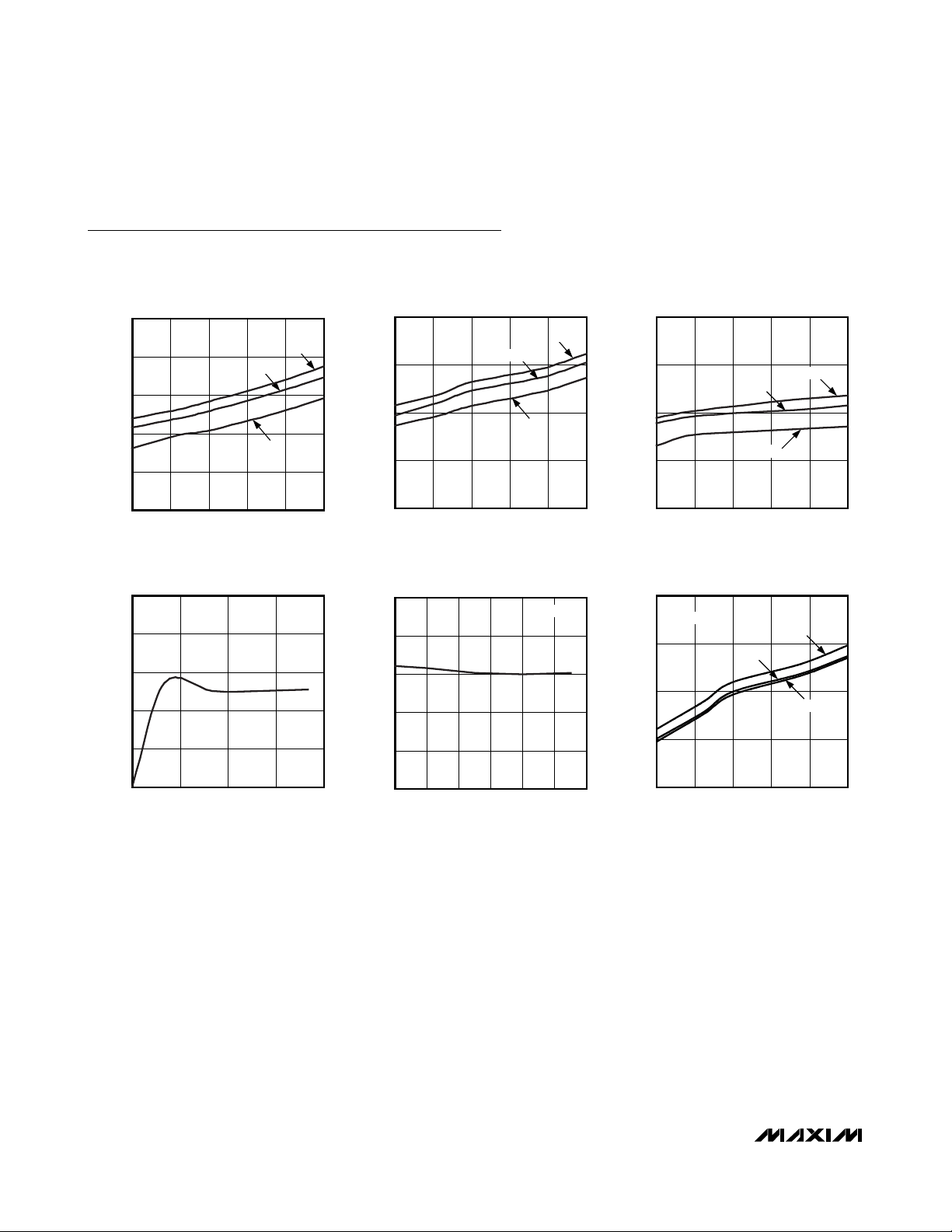
Typical Operating Characteristics
(TA = +25°C, unless otherwise noted.)
OPERATING SUPPLY CURRENT
vs. TEMPERATURE
MAX6960 toc01
TEMPERATURE (°C)
SUPPLY CURRENT (mA)
925926-7
7.2
7.4
7.6
7.8
8.0
7.0
-40 125
3.6V
3.3V
2.7V
SHUTDOWN SUPPLY CURRENT
vs. TEMPERATURE
MAX6960 toc02
TEMPERATURE (°C)
SUPPLY CURRENT (mA)
925926-7
0.1
0.2
0.3
0.4
0
-40 125
3.6V
3.3V
2.7V
DEAD-CLOCK OSCILLATOR
vs. SUPPLY VOLTAGE
MAX6960 toc03
SUPPLY VOLTAGE (V)
DEAD-CLOCK OSCILLATOR
3.383.162.942.72
85
90
95
100
80
2.50 3.60
+25°C
-40°C
+125°C
PEAK-OUTPUT SOURCE CURRENT
vs. SUPPLY VOLTAGE (HIGH-CURRENT MODE)
MAX6960 toc04
SUPPLY VOLTAGE (V)
PEAK-OUTPUT CURRENT (mA)
3.43.12.8
37
39
41
43
45
35
2.5 3.7
2.3V LED
PEAK-OUTPUT SOURCE CURRENT
vs.SUPPLY VOLTAGE (LOW-CURRENT MODE)
MAX6960 toc05
SUPPLY VOLTAGE (V)
PEAK-OUTPUT CURRENT (mA)
3.53.33.12.92.7
18
19
20
21
22
17
2.5 3.7
2.2V LED
PEAK-OUTPUT SOURCE CURRENT
vs. TEMPERATURE (HIGH-CURRENT MODE)
MAX6960 toc06
TEMPERATURE (°C)
PEAK-OUTPUT CURRENT (mA)
925926-7
39.6
40.0
40.4
40.8
39.2
-40 125
2.3V LED
3.6V
3.3V
3.15V
Typical Operating Characteristics
MAX6960–MAX6963
4-Wire Serially Interfaced
8 x 8 Matrix Graphic LED Drivers
_______________________________________________________________________________________ 5
Pin Description
PIN
MQFP TQFN
1, 6, 11,
12, 44
2–5, 7–10 2–5, 7–10 ROW1–ROW8 LE D C athod e D r i ver s. ROW 1 to RO W 8 outp uts si nk cur r ent fr om the d i sp l ay' s cathod e r ow s.
13 13 OSC Multiplex Clock Input. Drive OSC with a 1MHz to 8.5MHz CMOS clock.
14 14 CS
15 15 DIN Serial-Data Input. Data from DIN loads into the internal shift register on CLK's rising edge.
16 16 DOUT Serial-Data Output. The output is tri-state.
17 17 CLK Serial-Clock Input. On CLK's rising edge data shifts into the internal shift register.
18 18 RST
19, 20,
21,
23–27,
29–33,
35, 36,
37
22, 28,
34, 38
39 39 ADDOUT
40 40 ADDIN
41 41 ADDCLK
1, 6, 11,
12, 44
19, 20,
21,
23–27,
29–33,
35, 36,
37
22, 28,
34, 38
NAME FUNCTION
GND Ground
Chip-Select Input. Serial data is loaded into the shift register when CS is low. Data is
loaded into the data latch on CS's rising edge.
Reset Input. Hold RST low until at least 50ms after all interconnected MAX6960s are
powered up.
COL1–COL16
V+
LED Anode Drivers. COL1 to COL16 outputs source current into the display's anode
columns.
Positive Supply Voltage. Bypass V+ to GND with a single 47µF bulk capacitor per chip
plus a 0.1µF ceramic capacitor per V+.
Address-Data Output. Connect ADDOUT to ADDIN of the next MAX6960. Use ADDOUT of
the last MAX6960 as a plane change interrupt output.
Address-Data Input. For first MAX6960, connect ADDIN to V+. For other MAX6960s,
connect ADDIN to ADDOUT of the preceding MAX6960.
Address-Clock Input/Output. Connect ADDCLK of all MAX6960 drivers together, ensuring
that only one MAX6960's ADDIN input is connected to V+.
Digit 0 Current Setting. Connect RISET0 to GND to program all of digit 0's segment
42 42 RISET0
43 43 RISET1
— EP EP Exposed Pad on Package Underside. Connect to GND.
currents to 40mA. Leave RISET0 open circuit to program all of digit 0's segment currents
to 20mA. Connect RISET0 to GND through a fixed or variable resistor to adjust all of digit
0's segment currents between 20mA and 40mA.
Digit 1 Current Setting. Connect RISET1 to GND to program all of digit 1's segment
currents to 40mA. Leave RISET1 open circuit to program all of digit 1's segment currents
to 20mA. Connect RISET1 to GND through a fixed or variable resistor to adjust all of digit
1's segment currents between 20mA and 40mA.
MAX6960–MAX6963
4-Wire Serially Interfaced
8 x 8 Matrix Graphic LED Drivers
6 _______________________________________________________________________________________
Quick-Start Guide
Selecting the Appropriate Driver
The MAX6960–MAX6963 matrix LED drivers are available in four versions, with different levels of functionality
(Table 1). The two-part ID bits in the fault and device ID
register (Table 32) identify the driver type to the interface software. The ID bits may be of use if the same
panel software is used to drive more than one type of
display panel, because the software can automatically
detect the panel type.
This data sheet uses the generic name MAX6960 to refer
to the family of four parts MAX6960 through MAX6963,
unless there is a specific difference to discuss.
The purpose of this quick-start guide is to provide an
overview of the capabilities of the MAX6960 so that the
driver can be easily evaluated for a particular application, without fighting through a complex data sheet.
Terminology
• Pixel: One “point” on a display. Comprises one LED
for a monocolor display, two LEDs for an RGY display, and three LEDs for an RGB display.
• Monocolor: Display has only one color, typically red
for low-cost signs or orange for traffic signs. Varying
the current through the LED changes the intensity of
the red.
Table 1. Levels of Functionality
Table 2. Maximum Display Matrix on a Single 4-Wire Interface
Table 3. 4-Wire Interface Speed Requirements for Animation
*When operated per Figure 17.
AVAILABLE FUNCTIONS
PART
MAX6960 √√√ √ √ √None.
MAX6961 — √ — √ — √
MAX6962 √√—— √√
MAX6963 — √ —— — √
RGB 2
BITS PER
PIXEL*
RGB
1 BIT PER
PIXEL*
RGY
2 BITS PER
PIXEL
RGY
1 BIT PER
PIXEL
MONOCOLOR
2 BITS PER
PIXEL
MONOCOLOR
1 BIT PER
PIXEL
REGISTER LIMITATIONS
PI bit (bit D7) in global panel
configuration register is fixed at 0
(Table 22).
C bit (bit D6) in global panel
configuration register is fixed at 0
(Table 21).
C bit (bit D6) in global panel
configuration register is fixed at 0
(Table 21).
PI bit (bit D7) in global panel
configuration register is fixed at 0
(Table 22).
DISPLAY CONFIGURATION MAXIMUM PIXEL COUNT EXAMPLE MAXIMUM PANEL (PIXELS)
Monocolor 32,768 256 x 128
RGY 16,384 256 x 64
RGB 32,768 (3 buses required; see Figure 17) 128 x 85
256 DRIVERS ON 4-WIRE INTERFACE, 50 FRAMES PER SECOND UPDATE RATE
DISPLAY-MEMORY-ACCESS METHOD
8-bit indirect display memory addressing 1.64 3.28
24-bit direct display memory addressing 4.92 9.83
1-BIT-PER-PIXEL INTENSITY
CONTROL (Mbps)
2-BITS-PER-PIXEL INTENSITY
CONTROL (Mbps)

MAX6960–MAX6963
4-Wire Serially Interfaced
8 x 8 Matrix Graphic LED Drivers
_______________________________________________________________________________________ 7
• Bicolor: Literally means two color, and usually refers
to LEDs built with two LED dice of different colors,
typically red and green or red and orange/yellow.
• Tricolor: Literally means three color, and can refer to
LEDs built with three LED dice of different colors, typically red, green, and blue. The term is also used to
refer to a display built with bicolor LEDs, because there
are three main colors available (red, green, yellow).
• RGY: Display uses one red LED (R) and one green
LED (G) per pixel. When both red and green LEDs
are lit, the resulting color is yellow (Y). Varying the
current through the LEDs changes the intensity of the
pixel and changes the color from red through shades
of orange and yellow to green.
• RGB: Display uses one red LED (R), one green LED
(G), and one blue LED (B) per pixel. Varying the current through the LEDs changes the intensity of the
pixel and changes the color through many shades
limited by the current control resolution.
MAX6960 Applications
The MAX6960 is a multiplexed, constant-current LED
driver intended for high-efficiency indoor signage and
message boards.
The high efficiency arises because the driver operates
from a 3.3V nominal supply with minimal voltage headroom required across the driver output stages. The
problem of removing heat from even a small display is
therefore minimized.
The maximum peak LED drive current is 40mA, which
when multiplexed eight ways, provides an average current of 5mA per LED. This current drive is expected to
be adequate for indoor applications, but inadequate for
outdoor signs operating in direct sun.
The MAX6960 directly drives monocolor (typically red
or orange/yellow) or RGY (typically red/green or
red/yellow) graphic displays using LEDs with a forward
voltage drop up to 2.5V. Blue LEDs and some green
LEDs cannot be driven directly because of their high
forward voltage drop (around 3.5V to 4.5V). For these
displays, the MAX6960 can be used as a graphic controller, just as it can be used for applications requiring
higher peak segment currents, and in RGB panels
needing a higher driver voltage for the blue LEDs. In
these cases, the MAX6960 can be used with external
drive transistors to control anode-row displays, with all
driver features including pixel-level intensity control still
available (see the Applications Information section and
Figure 17).
Display Intensity Control
Five levels of intensity control are provided:
• A 256-step PWM panel intensity adjustment sets all
MAX6960s simultaneously as a global panel brightness control (Table 27). The 256-step resolution is
fine enough to allow fade-in/fade-out graphic effects,
as well as provide a means for compensating a
panel for background lighting.
• A 2-bits-per-pixel intensity control allows four brightness levels to be set independently per pixel. The
pixel-level intensity control can be set to be either
arithmetic (off, 1/3, 2/3, full) or geometric (off, 1/4,
1/2, full) for full flexibility (Table 24), and allows four
colors to be displayed on monocolor panels, or 16
colors to be displayed on RGY panels, or 64 colors
to be displayed on RGB panels.
• The LED drive current can be selected between
either a 40mA peak per segment and a lower 20mA
peak current on a digit-by-digit basis using the
R
ISET0
and R
ISET1
pins. The lower (20mA) current
may be the better choice to drive high-efficiency displays, and this setting allows the MAX6960 to operate from a supply voltage as low as 2.7V.
• The LED drive current can be adjusted between
40mA and 20mA peak current on a digit-by-digit
basis using fixed or adjustable resistors connected
from the R
ISET0
and R
ISET1
pins to GND. These controls enable analog relative adjustments in digit
intensity, typically to calibrate digits from different
batches, or to color balance RGY displays.
• The digit intensity controls allow each digit’s operating current to be scaled down in 256 steps from the
global panel intensity adjustment. The effective operating current for each digit becomes n/256th of the
panel intensity value. These controls enable digital
relative adjustments in digit intensity in addition to
the analog approach outlined above.
Display Size Limitations
The maximum display size that can be handled by a
single 4-wire serial interface is given in Table 2, which
is for the maximum 256 interconnected MAX6960s.
Larger display panels can be designed using a separate CS line for each group of (up to) 256 MAX6960s.
Each group would also have its own local 3-wire bus to
allocate the driver addresses. The 4-wire interface
speeds requirement when continuously updating display memory for high-speed animations is given in
Table 3.
MAX6960–MAX6963
4-Wire Serially Interfaced
8 x 8 Matrix Graphic LED Drivers
8 _______________________________________________________________________________________
Software Control
The hardware features are designed to simplify the
software interface and eliminate software timing dependencies:
• Two or four planes of display memory are stored,
allowing images to be preloaded into the MAX6960–
MAX6963 frame memory.
• Animation timing is built in, sequencing through the
two or four planes automatically. System software
has to update the upcoming plane(s) with new data
ahead of time, but do not be concerned about exact
timing. The frame rate is adjustable to as fast as 63
frames a second for animations, or to as slow as one
frame change every 63s for advertising sequencing.
• Multiple MAX6960s interconnect and share display
memory so that the software “sees” the display as
memory-mapped planes of contiguous RAM.
• Global commands that need to be received and
acted on by every MAX6960 in a panel do just that,
with one write.
Hardware Design
A MAX6960 normally drives an 8 x 16 LED matrix, comprising 8 cathode rows and 16 anode columns, or
8 anode rows and 16 cathode columns with external
drivers.
The MAX6960 standard wiring connection to either two
monocolor 8 x 8 digits, or to a single RGY 8 x 8 digit is
shown in Table 4. Figure 3 shows the display pin naming.
Figures 1 and 2 show example displays with the
MAX6960 drivers connecting to monocolor and RGY panels. Figure 4 shows how the display memory maps to the
physical pixels on the display panel, provided that the
MAX6960 drivers are interconnected correctly in a rasterlike manner from top left of the panel to bottom right.
Detailed Description
Overview
The MAX6960 is an LED display driver capable of driving
either two monocolor 8 x 8 cathode-row matrix digits, or a
single RGY 8 x 8 cathode-row matrix digit. The architecture of the driver is designed to allow a large graphic
Table 4. Standard Driver Connection to Monocolor and RGY 8 x 8 Displays
*Digit 0 of a monocolor display is called red, and digit 1 is called green in the data sheet.
Figure 1. Monocolor 1-Bit-per-Pixel, 96-Pixel x 32-Pixel Display Example
DRIVER PINS ROW1–ROW8 DRIVER PINS COL1–COL8 DRIVER PINS COL9–COL16
Monocolor digit 0 (red*)
Monocolor digit 1 (green*)
RGY red/green
Digit 0 (red*) rows (cathodes)
R1 to R8
Digit 1 (green*) rows
(cathodes) R1 to R8
Red/green rows (cathodes) R1
to R8
Digit 0 columns (anodes) C1 to
C8
—
Red columns (anodes) C1 toC8Green columns (anodes) C1 to
—
Digit 1 columns (anodes) C1 to
C8
C8
DRIVER0
RED
DRIVER6
RED
RED RED
RED RED
DRIVER1
DRIVER7
DRIVER2
RED RED
DRIVER8
RED RED
DRIVER12
RED
DRIVER18
RED
RED RED
RED RED
DRIVER13
DRIVER19
DRIVER14
RED RED
DRIVER20
RED RED
DRIVER3
RED RED
DRIVER9
RED RED
DRIVER15
RED RED
DRIVER21
RED RED
RED RED
RED RED
RED RED
RED RED
DRIVER4
DRIVER10
DRIVER16
DRIVER22
RED RED
RED RED
RED RED
RED RED
DRIVER5
RED
DRIVER11
RED
DRIVER17
RED
DRIVER23
RED
MAX6960–MAX6963
4-Wire Serially Interfaced
8 x 8 Matrix Graphic LED Drivers
_______________________________________________________________________________________ 9
display panel to be driven easily and intuitively by multiple MAX6960s using 8 x 8 cathode-row matrix digits. The
MAX6960s in a display-driver design not only share the
host 4-wire interface, but they also share a local 3-wire
interface that is not connected to the host. The local 3wire interface works with the user’s driver settings to configure all the MAX6960s to appear to the host interface as
one contiguous memory-mapped driver.
The pixel level-intensity control uses frame modulation.
Pixels are enabled and disabled on a frame-by-frame
basis over a 12-frame super frame (Table 5). The effective pixel frame duty cycle within a super frame sets each
pixel’s effective intensity. The 12-frame period of a super
frame allows arithmetic and geometric intensity scales to
be mixed on the same driver. This allows the user to set
up an RGY display with a different color scale for red and
Figure 2. RGY 1-Bit-per-Pixel 48-Pixel x 32-Pixel Display Example
Figure 3. 8 x 8 Matrix Pin Assignment
Figure 4. How Plane Memory Across Multiple
MAX6960–MAX6963 Maps to Display Pixels
DRIVER0
RED
GREEN GREEN GREEN GREEN GREEN GREEN
DRIVER1
RED
DRIVER2
RED
DRIVER3
RED
DRIVER4
RED
DRIVER5
RED
DRIVER6
RED
GREEN GREEN GREEN GREEN GREEN GREEN
DRIVER12
RED
GREEN GREEN GREEN GREEN GREEN GREEN
DRIVER18
RED
GREEN GREEN GREEN GREEN GREEN GREEN
DRIVER7
RED
DRIVER13
RED
DRIVER19
RED
DRIVER8
RED
DRIVER14
RED
DRIVER20
RED
COLUMN 1
COLUMN 2
COLUMN 3
COLUMN 4
COLUMN 5
COLUMN 6
COLUMN 7
ROW 1
ROW 2
ROW 3
ROW 4
ROW 5
ROW 6
ROW 7
ROW 8
MONOCOLOR
RED
RED
RED
COLUMN 8
ROW 1
ROW 2
ROW 3
ROW 4
ROW 5
ROW 6
ROW 7
ROW 8
DRIVER9
DRIVER15
DRIVER21
DRIVER10
RED
DRIVER16
RED
DRIVER22
RED
COLUMN 1 (RED)
COLUMN 9 (GREEN)
RGY
DRIVER11
RED
DRIVER17
RED
DRIVER23
RED
FIRST DISPLAY PIXEL
MAPS TO FIRST PLANE
LAST DISPLAY PIXEL
MAPS TO LAST PLANE
MEMORY LOCATION
MAX6960–MAX6963
4-Wire Serially Interfaced
8 x 8 Matrix Graphic LED Drivers
10 ______________________________________________________________________________________
green. The MAX6960 uses display memory planes to
store the display images. A memory plane is the exact
amount of memory required to store the display image.
The memory plane architecture allows one plane to be
used to refresh the display, while at least one other plane
is available to build up the next image. The global plane
counter register (Table 30) allows the plane used to
refresh the display to be selected either directly on command, or automatically under MAX6960 control.
Automatic plane switching can be set from 63 plane
changes a second to one plane change every 63s.
Display Memory Addressing
The MAX6960 contains 64 bytes of display mapping
memory. This display memory provides four memory
planes (of 16 bytes) when 1-bit-per-pixel intensity control is selected, or two memory planes (of 32 bytes)
when 2-bits-per-pixel intensity control is used (Table 6).
The 64 bytes of display memory in a MAX6960 could
be accessed with 6 bits of addressing on a driver-bydriver basis.
The MAX6960 uses a 14-bit addressing scheme. The
address map encompasses up to 256 MAX6960 drivers, all connected to the host through a common 4wire interface, and also interconnected through a local
3-wire interface. The purpose of the 3-wire interface is
to actively segment the 14-bit address space among
the (up to) 256 MAX6960s.
The total display memory is already partitioned among
these MAX6960 drivers in a register format. The
MAX6960s repartition these registers to appear as contiguous planes of display memory, organized by color
(red, then green) and then into planes (P0 to P4)
(Table 6).
Register Addressing Modes
The MAX6960 accepts 8-bit, 16-bit, and 24-bit transmissions. All MAX6960s sharing an interface receive
and decode all these transmissions, but the content of
a transmission determines which MAX6960s store and
use a particular transmission, and which discard it
(Table 7).
Table 5. Frame Modulation with Pixel Intensity
Table 6. Panel Configuration
PIXEL
GRADUATION
Both 1 1 Full 1 1 1 1 1 1 1 1 1 1 1 1
Arithmetic 1 0 2/3 1 0 1 1 0 1 1 0 1 1 0 1
Geometric 1 0 1/2 1 0 1 0 1 0 1 0 1 0 1 0
Arithmetic 0 1 1/3 0 1 0 0 1 0 0 1 0 0 1 0
Geometric 0 1 1/4 0 1 0 0 0 1 0 0 0 1 0 0
Both 0 0 Off 0 0 0 0 0 0 0 0 0 0 0 0
BIT BIT
PIXEL
INTENSITY
SETTING
GLOBAL PANEL CONFIGURATION
REGISTER
PLANES/INTENSITY
(PI BIT)
0 0 1 bit per pixel Monocolor 16 red contiguous 4
0 1 1 bit per pixel RGY
1 0 2 bits per pixel Monocolor
COLOR
(C BIT)
PIXEL-LEVEL
INTENSITY
CONTROL
PATTERN OF MULTIPLEX CYCLES FOR WHICH A PIXEL IS ENABLED
01234567891011
DISPLAY TYPE
DISPLAY MAPPING
ADDRESSES PER PLANE
8 red contiguous,
8 green contiguous
16 red contiguous,
16 red contiguous
DISPLAY
PLANES
AVAILABLE
4
2
1 1 2 bits per pixel RGY
16 red
(2 noncontiguous groups of 8),
16 green
(2 noncontiguous groups of 8)
2
MAX6960–MAX6963
4-Wire Serially Interfaced
8 x 8 Matrix Graphic LED Drivers
______________________________________________________________________________________ 11
8-Bit Transmissions
Eight-bit transmissions are write-only, data-only
accesses that write data to the display memory indirected by the global display indirect address register
(Figure 6). The global display indirect address register
autoincrements after the write access. Eight-bit transmissions provide the quickest method of updating a
plane of display memory of the MAX6960. It is the most
suitable display update method if the host system
builds an image in local memory, and then dumps the
image into a display plane of the MAX6960.
16-Bit Transmissions
Sixteen-bit transmissions are read/write, commandand-data accesses to the MAX6960’s configuration
registers (Figure 7). A write can generally be global
(updates all MAX6960s on the 4-wire bus with the same
data) or specific (updates just the MAX6960 indirected
by the global driver indirect address register). Note:
The global driver indirect address register selects a
specific MAX6960. This is not the same as the global display indirect address register, which points to
display memory that could be in any MAX6960. A
16-bit read is always indirected through the global driver indirect address register to select only one
MAX6960 to respond. When a read or write is indirected through the global driver indirect address register,
the 16-bit command can choose whether the global driver indirect address is autoincremented after the command has been executed. This allows the host to set up
one or more registers in consecutive MAX6960s with
the display indirect address, autoincrementing only
when required.
Table 7. Register Addressing Modes
8-, 16-, OR 24-BIT DATA PACKET SENT TO MAX6960
DATA FORMAT
D23
D22
D21
D20
D19
D18
D17
D16
D15
D14
8-bit indirect display
memory addressing.
Address is global display
indirect address (14 bits)
stored as {MSB, LSB} in
{register 0x0A, register
0x09}.
16-bit device addressing. — R/W AI L/G 0
Factory reserved; do not
write to this address.
24-bit direct display
memory addressing
(monocolor 1 bit per
pixel).
24-bit direct display
memory addressing
(RGY 1 bit per pixel).
R/W X
R/W X
Planes
0, 1, 2, 3
Planes
0, 1, 2, 3
—1 —
12-bit addressing across 256 drivers,
4096 x 8 red pixels
12-bit addressing across 256 drivers,
2048 x 8 red pixels, and
2048 x 8 green pixels
— 8 bits of display memory
D13
D12
D11
D10
4-bit
address
D9
D8
D7
D6
D5
8 bits of driver register data
8 bits of display memory
(1 bit per pixel)
8 bits of display memory
(1 bit per pixel)
D4
D3
D2
D1
D0
24-bit direct display
memory addressing
(monocolor 2 bits per
pixel).
24-bit direct display
memory addressing
(RGY 2 bits per pixel).
R/W X
R/W X
Planes
0, 1
Planes
0, 1
13-bit addressing across 256 drivers,
4096 x 4 red pixels
13-bit addressing across 256 drivers,
4096 x 4 red pixels, and
4096 x 4 green pixels
8 bits of display memory
(2 bits per pixel)
8 bits of display memory
(2 bits per pixel)

MAX6960–MAX6963
4-Wire Serially Interfaced
8 x 8 Matrix Graphic LED Drivers
12 ______________________________________________________________________________________
24-Bit Transmissions
Twenty-four-bit transmissions are read/write, addressand-data accesses to the MAX6960’s display memory
(Figure 8). This is direct access to display memory
because the memory address is included in the 24-bit
transmission, compared with an 8-bit transmission,
which uses the memory address stored in the global
display indirect address register. Twenty-four-bit transmissions provide the random-access method of updating a plane of display memory of the MAX6960. It is the
most suitable display update method if the host system
builds an image directly in a display memory plane,
rather than in host local memory.
Host 4-Wire Serial Interface
Serial Addressing
The MAX6960 communicates to the host through a 4wire serial interface. The interface has three inputs:
clock (CLK), chip select (CS), and data in (DIN), and
one output, data out (DOUT). CS must be low to clock
data into the device, and DIN must be stable when
sampled on the rising edge of CLK. DOUT is used for
read access, and is stable on the rising edge of CLK.
DOUT is high impedance except during MAX6960 read
accesses. Multiple MAX6960s may be connected to the
same 4-wire interface, with all devices connected to all
four interface lines in parallel. The normal limit of paralleled MAX6960s is 256, because that is the interconnection limit for the 3-wire interface and associated
device addressing. The Applications Information section discusses some practical issues raised by driving
many devices in parallel from the same interface.
The serial interface responds to only 8-bit, 16-bit, and
24-bit commands (Table 7).
The MAX6960 ignores any transmission that is not
exactly 8 bits, 16 bits, or 24 bits between the falling
and subsequent rising edge of CS.
Control and Operation Using the 4-Wire Interface
Controlling the MAX6960 requires sending an 8-bit, 16bit, or 24-bit word. The last byte, D7 through D0, is
always the data byte. Eight-bit accesses are write-only
accesses; 16-bit or 24-bit accesses are read or write
accesses, as determined by the MSB of the transmission, which is set for a read access; clear for a write. A
16-bit or 24-bit read involves transmitting 16 or 24 bits
to DIN, taking CS high, and then reading back 8 bits
from DOUT. Only one MAX6960’s DOUT is enabled
from tri-state for readback. The selected MAX6960’s
DOUT normally returns to tri-state after the 8th falling
edge of CLK. However if CS falls during the read
before the 8th falling edge of CLK, then the readback is
terminated and the selected MAX6960’s DOUT returns
to tri-state.
If a number of bits other than exactly 8 bits, 16 bits, or
24 bits are clocked into the MAX6960 between taking
CS low and taking CS high again, then that transmission is ignored.
Writing Device Registers
The MAX6960 is written to using the following
sequence (Figures 3, 4, and 5):
1) Take CLK low.
2) Take CS low.
3) For an 8-bit transmission:
Clock 8 bits of data into DIN, D7 first to D0 last,
observing the setup and hold times.
For a 16-bit transmission:
Clock 16 bits of data into DIN, D15 first to D0 last,
Figure 5. Timing Diagram
CS
CLK
DIN
DOUT
t
CSS
t
DS
Dn Dn-1
t
DH
tCLt
CH
D1 D0
t
CSH
t
CP
t
DO
D7 D6 D1 D0
t
CSW
t
DO
t
DO
.

MAX6960–MAX6963
4-Wire Serially Interfaced
8 x 8 Matrix Graphic LED Drivers
______________________________________________________________________________________ 13
CLK
Figure 6. 8-Bit Write to the MAX6960–MAX6963
Figure 7. 16-Bit Write to the MAX6960–MAX6963
Figure 8. 24-Bit Write to the MAX6960–MAX6963
CS
DIN
DOUT
D7 D6 D5 D4 D3 D2 D1 D0
TRI-STATE
CS
CLK
D15
DIN
DOUT
TRI-STATE
D14 D13 D12 D11 D10 D9 D8 D7 D6 D5 D4 D3 D2 D1 D0
= 0
.
CS
CLK
D23
DIN
DOUT
TRI-STATE
D22 D21 D20 D19 D18 D7 D6 D5 D4 D3 D2 D1 D0
= 0
D14 D13 D12 D11 D10 D9 D8D16 D15D17
.

MAX6960–MAX6963
4-Wire Serially Interfaced
8 x 8 Matrix Graphic LED Drivers
14 ______________________________________________________________________________________
observing the setup and hold times. Bit D15 is low,
indicating a write command.
For a 24-bit transmission:
Clock 24 bits of data into DIN, D23 first to D0 last,
observing the setup and hold times. Bit D23 is low,
indicating a write command.
4) Take CS high (while CLK is still high after clocking
in the last data bit).
5) Take CLK low.
Reading Device Registers
Any register data within the MAX6960 may be read by
sending a logic-high to bit D15. The sequence is:
1) Take CLK low.
2) Take CS low.
3) For a 16-bit transmission:
Clock 16 bits of data into DIN, D15 first to D0 last,
observing the setup and hold times. Bit D15 is high,
indicating a read command. Bits D7 to D0 are
dummy bits, and are discarded by the MAX6960.
For a 24-bit transmission: Clock 24 bits of data into
DIN, D23 first to D0 last, observing the setup and
hold times. Bit D23 is high, indicating a read command. Bits D7 to D0 are dummy bits, and are discarded by the MAX6960.
4) Take CS high (while CLK is still high after clocking
in the last data bit).
5) Take CLK low.
6) The selected MAX6960’s DOUT is enabled from tristate for read back.
7) Clock 8 bits of data from DOUT, D7 first to D0 last,
observing the setup and hold times.
8) Take CLK low after the final (8th) data bit.
The selected MAX6960’s DOUT returns to tri-state.
Figure 10 shows a read operation when 24 bits are
transmitted and 8 bits are read back.
Local 3-Wire Serial Interface
The MAX6960 uses a 3-wire interface to bus together
up to 256 MAX6960s. The 3-wire bus enables each
device to calculate its own unique driver address
(0 to 255), and reconfigure its display memory. The
ADDOUT output also provides an interrupt at every
page change, when the plane counter is configured to
automatic (Table 30).
Figure 9. 16-Bit Read from the MAX6960–MAX6963
Figure 10. 24-Bit Read from the MAX6960–MAX6963
CS
CLK
D15
D14 D13 D12 D11 D10 D9 D8 D0
= 1
DOUT
DIN
TRI-STATE
CS
CLK
D23
DOUT
DIN
D22 D21 D20 D19 D18 D7 D6 D5 D4 D3 D2 D1
= 1
TRI-STATE
D14 D13 D12 D11 D10 D9 D8D16 D15D17 D0
D7 D6 D5 D4 D3 D2 D1
D7 D6 D5 D4 D3 D2 D1 D0
D7 D6 D5 D4 D3 D2 D1 D0
.
.

MAX6960–MAX6963
4-Wire Serially Interfaced
8 x 8 Matrix Graphic LED Drivers
______________________________________________________________________________________ 15
3-Wire Interface Data Lines
(ADDOUT and ADDIN)
One MAX6960 is designated the master device, and this
is allocated driver address 0. The master’s ADDIN pin is
connected to V+, identifying it as the first device. This
first MAX6960 should be the driver for the top-left pix-
els of the display panel. The master’s
ADDOUT pin is connected to the second MAX6960’s
ADDIN pin, and that MAX6960’s ADDOUT pin is connected to the third MAX6960’s ADDIN, and so on up to 256
MAX6960s. The last MAX6960’s ADDOUT pin is left open
circuit. The last MAX6960 should be the driver for the
bottom-right pixels of the display panel. The ADDOUT
is initialized low at the start of a 3-wire interface configuration operation, and goes high (N + 1.5) ADDCLK periods
later, where n is the driver address of the MAX6960 (0 to
255). See Figures 1 and 2 for connection examples.
3-Wire Interface Clock (ADDCLK)
The ADDCLK pins for all MAX6960s are all connected
together. ADDCLK data rate is determined by OSC / 4,
nominally 1.048576 MHz. The ADDCLK pin for the master
MAX6960 (driver address 0) is always an output, and all
the other ADDCLKs are always inputs. ADDCLK is active
for exactly 256 clock cycles when a panel configuration is
being performed (on power-up reset, and after a write to
the global panel configuration register).
Use of ADDOUT as Plane Change Interrupt
(IRQ)
When the plane counter is configured to automatic mode
(bit 6 of the global plane counter register is set) (Table
30), ADDOUT pulses low for a time of 512/OSC (nominally
122µs) at the start of every automatic plane change. This
signal can be used as an interrupt output from the display
panel to the host to flag that the previous display plane is
now unused and can be written with a new image.
Multiplex Clock
The OSC input for all MAX6960s sharing a 3-wire interface
bus (but not necessarily a 4-wire interface bus) should be
driven by a common CMOS-level clock ranging between
1MHz and 8.5MHz. It is usually necessary to use an external clock tree to fan out multiple clock drives when larger
numbers of MAX6960s are used because of the capacitive loads. For example, each one of the eight outputs of a
standard 74HC541 octal buffer could drive 8 to 32
MAX6960 OSC inputs, depending on the layout used.
The recommended setting for OSC is 4.194303MHz. This
frequency sets the slow global plane counter resolution to
1s, and the fast global plane counter resolution to 1Hz.
Table 8. Register Address Map
*When reading from the global registers, only the master MAX6960 (whose driver address is 0x00) responds.
REGISTER
D15 D14 D13 D12 D11 D10 D9 D8
Driver Address (read only) X X 0000 0x00
Pixel Intensity Scale X 0001 0x01
Panel Intensity X 0010 0x02
Digit 0 Intensity X 0011 0x03
Digit 1 Intensity X 0100 0x04
Fault X 0101 0x05
— X0110 0x06
—
Global Driver Indirect Address* X X X 1000 0x08
Global Display Indirect Address LSB* X X X 1001 0x09
Global Display Indirect Address
Global Plane Counter* X X X 1011 0x0B
Global Clear Planes* X X X 1100 0x0C
Global Panel Configuration* X X X 1101 0x0D
Global Driver Devices*
Global Driver Rows* X X X 1111 0x0F
R/W
COMMAND ADDRESS
Autoincrement
XXX1010 0x0A
XXX1110 0x0E
Local/Global
X0111 0x07
HEX CODE

MAX6960–MAX6963
4-Wire Serially Interfaced
8 x 8 Matrix Graphic LED Drivers
16 ______________________________________________________________________________________
Global and Local Register
Addressing
The register map (Table 8) contains three local registers and eight global registers. Global registers are
always written to in all MAX6960s (on the same 4-wire
interface) at the same time, using a 16-bit transmission.
A read from a global register also always results in a
read from driver address 0. The global nature of these
registers ensures that all drivers work together, and
there is no chance of a software miss-send causing, for
example, multiple MAX6960s to try to transmit on the 4wire DOUT line at the same time.
The three local registers can be written to on an individ-
ual basis (updates just the MAX6960 indirected by the
global driver indirect address register), or on a global
basis (updates all MAX6960s), according to the status
of the local/global bit (Table 9). The local/global bit is
ignored during a 16-bit read transmission, and the
MAX6960 pointed to by the global driver indirect
address register is read.
Register Address Autoincrementing
When a read or write is indirected through the global driver indirect address register, the 16-bit command can
choose whether the global driver indirect address is
autoincremented after the command has been executed.
Table 9. Register Address Local/Global Control Bit Format
Table 10. Register Address Autoincrement Control Bit Format
Table 11. Driver Address Register Format
ADDRESS
REGISTER
LOCAL: Only the MAX6960 indirected by driver
indirect address is written.
GLOBAL: All MAX6960s are written with the same
data.
LOCAL: The MAX6960 indirected by driver indirect
address responds.
GLOBAL: The MAX6960 configured to address 0x00
responds.
GLOBAL: All MAX6960s are written with the same
data.
GLOBAL: The MAX6960 configured to address 0x00
responds.
CODE
(HEX)
0x00 to
0x07
0x08 to
0x0F
D15 D14 D13 D12 D11 D10 D9 D8
0X0XXXXX
0X1XXXXX
1X0XXXXX
1X1XXXXX
0XXXXXXX
1XXXXXXX
ADDRESS
REGISTER
Driver indirect address is not changed X 0 XXXXXX
Driver indirect address is incremented after read/write
Driver indirect address is not changed
CODE
(HEX)
0x00 to
0x07
0x08 to
D15 D14 D13 D12 D11 D10 D9 D8
X1XXXXXX
XXXXXXXX
COMMAND ADDRESS
COMMAND ADDRESS
ADDRESS
REGISTER
Driver address 0x00 MSB 8-bit driver address 0x00 to 0xFF LSB
CODE
(HEX)
D7 D6 D5 D4 D3 D2 D1 D0
REGISTER DATA

This allows the host to set up one or more registers in
consecutive MAX6960s with the display indirect address,
autoincrementing only when required (Table 10).
Driver Address Register
Reading the driver address register (Table 11) returns
the driver address that has been assigned to a particular MAX6960. The order of the driver addresses is
determined purely by the order that the 3-wire interface
is daisy-chained through multiple MAX6960s. The register is used to detect the presence of a MAX6960 at an
address, and a binary search on the 256 possible
addresses can be used to determine the size of an
array of MAX6960s.
MAX6960–MAX6963
4-Wire Serially Interfaced
8 x 8 Matrix Graphic LED Drivers
______________________________________________________________________________________ 17
Table 13. Global Driver Devices Format
Table 14. Global Driver Rows Format
Table 12. Power-Up Configuration
*When reading from the global registers, only the master MAX6960 (whose driver address is 0x00) responds.
REGISTER FUNCTION POWER-UP CONDITION
Driver address (read only) Address 0 0x00 0 0 000000
Pixel intensity scale Arithmetic for red and green 0x01 X X XXXX00
Panel intensity 128/256 intensity 0x02 1 0 000000
Digit 0 intensity Full 255/256 0x03 1 1 111111
Digit 1 intensity Full 255/256 0x04 1 1 111111
Fault No faults 0x05 0 X XXXX00
Global driver indirect address Address 0x00 0x08 0 0 000000
Global display indirect address
LSB
Global display indirect address
MSB
Global plane counter Manual selection to plane 0 0x0B 0 0 000000
Global panel configuration
Global driver devices 256 drivers interconnected 0x0E 1 1 111111
Global driver rows 256 drivers in a row 0x0F 1 1 111111
Address 0x0000
Shutdown mode,
ripple sync enabled,
mux flip enabled,
color is mono,
4 display planes/1 bit per
pixel
ADDRESS
CODE (HEX)
0x09 0 0 000000
0x0A X X 000000
0x0D 0 0 1 1 X X X 0
D7 D6 D5 D4 D3 D2 D1 D0
REGISTER DATA
REGISTER
Global driver devices 0x0E
ADDRESS
CODE (HEX)
D7 D6 D5 D4 D3 D2 D1 D0
MS
8-bit global driver devices 0x00 to 0xFF LSB
REGISTER DATA
REGISTER
Global driver rows 0x0F MSB 8-bit global driver rows 0x00 to 0xFF LSB
ADDRESS
CODE (HEX)
D7 D6 D5 D4 D3 D2 D1 D0
REGISTER DATA

MAX6960–MAX6963
Initial Power-Up
The power-up sequence consists of an internal power-on
reset (POR), assertion of the external reset input RST,
and auto-address configuration (see the Local 3-Wire
Interface section). The internal POR resets all control
registers to the default values shown in Table 12.
After RST goes high an internal timer delays execution of
the auto-address configuration for 221(2,097,152) OSC
cycles (nominally 250ms at OSC = 4.194MHz) (see the
3-Wire Interface Clock (ADDCLK) section). During this
delay time, the global driver devices register (0x0E),
global driver rows register (0x0F), and global panel configuration register (0x0D) should be written as these
values are used in the auto-address configuration
sequence (see the Device Configuration section). After
the internal delay time, the auto-addressing configuration
commences and takes a fixed interval of 256 ADDCLK
cycles to complete where the ADDCLK frequency is
OSC/4 (see the 3-Wire Interface Clock (ADDCLK) section). After completing the auto-self-addressing of all
possible 256 interconnected devices, all of the
MAX6960s enter shutdown mode.
All registers are capable of write device register operations during the internal delay interval using the 4-wire
serial interface. Read device register operations are not
allowed during auto-address configuration.
4-Wire Serially Interfaced
8 x 8 Matrix Graphic LED Drivers
18 ______________________________________________________________________________________
Table 15. Global Panel Configuration Register Format
Table 16. Global Panel Configuration—Shutdown Control (S Data Bit D0) Format
Table 17. Global Panel Configuration—Invert Pixels (IP Data Bit D1) Format
Table 18. Global Panel Configuration—Current Plane (DP0, DP1 Data Bit D2, D3) Format
REGISTER
Global panel configuration 0x0D PI C F R DP1 DP0 IP S
ADDRESS
CODE (HEX)
D7 D6 D5 D4 D3 D2 D1 D0
REGISTER DATA
REGISTER
Shutdown 0x0D PI C F R DP1 DP0 IP 0
Normal operation 0x0D PI C F R DP1 DP0 IP 1
ADDRESS
CODE (HEX)
D7 D6 D5 D4 D3 D2 D1 D0
REGISTER DATA
REGISTER
Logic 1 in display memory lights the appropriate
LED (normal logic)
Logic 0 in display memory lights the appropriate
LED (invert logic)
ADDRESS
CODE (HEX)
0x0D PI C F R DP1 DP0 0 S
0x0D PI C F R DP1 DP0 1 S
D7 D6 D5 D4 D3 D2 D1 D0
REGISTER DATA
REGISTER
Current display plane is P0 0x0D PI C F R 0 0 IP S
Current display plane is P1 0x0D PI C F R 0 1 IP S
Current display plane is P2 0x0D 0 C F R 1 0 IP S
Current display plane is P0 0x0D 1 C F R 1 0 IP S
Current display plane is P3 0x0D 0 C F R 1 1 IP S
Current display plane is P1 0x0D 1 C F R 1 1 IP S
ADDRESS
CODE (HEX)
D7 D6 D5 D4 D3 D2 D1 D0
REGISTER DATA

Device Configuration
The MAX6960s driving a display panel must be configured before the panel can be used to display images.
The configuration involves the global panel configuration register (Table 15–Table 22), the global driver
devices register (Table 13), and the global driver rows
register (Table 14). The global driver devices register
should be written with the total number of MAX6960s
interconnected on the 3-wire interface, minus 1 (Table
13). For the four panel examples shown in Figures 1
and 2, 24 MAX6960s are used, so the global driver
devices register should be written with the value 23, or
0x17.
The global driver rows register should be written with
the number of MAX6960s per panel row, minus 1
(Table 14). For the panel examples shown in Figure 1
and Figure 2, there are six MAX6960s per row, so the
global driver rows register should be written with the
value 5.
The values stored in the global driver devices register
and the global driver rows register, together with the C
and Pl bits in the global panel configuration register
(Tables 21 and 22), are used by the 3-wire interface
configuration engine to reconfigure display memory
addressing among the interconnected MAX6960s.
Global Panel Configuration Register
The global panel configuration register contains eight
device settings (Table 15 to Table 22).
Shutdown Mode (Bit D0)
Shutdown mode is exited by clearing the S bit in the
global panel configuration register (Table 16). When
the MAX6960 is in shutdown mode, LED driver outputs
ROW1–ROW8 and COL1–COL16 are tri-stated, and
multiplexing is halted. Data in the global configuration
registers remains unaltered. For minimum supply current in shutdown mode, logic inputs should be at GND
or V+ potential. Shutdown mode is exited by setting the
S bit in the global panel configuration register.
Invert Pixels (Bit D1)
The invert pixels (IP) bit in the global panel configuration register controls whether the display memory is
used directly or inverted (Table 17).
MAX6960–MAX6963
4-Wire Serially Interfaced
8 x 8 Matrix Graphic LED Drivers
______________________________________________________________________________________ 19
Table 19. Global Panel Configuration—Ripple Sync Control (R Data Bit D4) Format
Table 20. Global Panel Configuration—Mux Flip Control (F Data Bit D5) Format
REGISTER
Ripple sync is disabled; all interconnected
MAX6960s on the same 4-wire bus resynchronize
together.
Ripple sync is enabled; all interconnected
MAX6960s on the same 4-wire bus resynchronize
with a 0.9537µs delay between adjacent devices.
ADDRESS
CODE (HEX)
0x0D PI C F 0 DP1 DP0 IP S
0x0D PI C F 1 DP1 DP0 IP S
D7 D6 D5 D4 D3 D2 D1 D0
REGISTER DATA
REGISTER
Mux flip is disabled: all interconnected MAX6960s
on the same 3-wire bus resynchronize to the
multiplex timing shown in Figure 11.
Mux flip is enabled: all interconnected MAX6960s on
the same 3-wire bus resynchronize with MAX6960s
with even driver addresses (0, 2, 4 to 254) operating
to the multiplex timing shown in Figure 11, and
MAX6960s with odd driver addresses (1, 3, 5 to 255)
operating to the flipped multiplex timing shown in
Figure 12.
ADDRESS
CODE (HEX)
0x0D PI C 0 R DP1 DP0 IP S
0x0D PI C 1 R DP1 DP0 IP S
D7 D6 D5 D4 D3 D2 D1 D0
REGISTER DATA

MAX6960–MAX6963
4-Wire Serially Interfaced
8 x 8 Matrix Graphic LED Drivers
20 ______________________________________________________________________________________
Table 21. Global Panel Configuration—Color Control (C Data Bit D6) Format
Table 22. Global Panel Configuration—Planes/Intensity Control (PI Data Bit D7) Format
Table 23. Frame Modulation with Pixel Intensity
Table 24. Pixel Intensity Scale Register Format
REGISTER
Display panel is built with monocolor or RGB
digits (permanently set this way for MAX6962 and
MAX6963)
Display panel is built with RGY digits
ADDRESS
CODE (HEX)
0x0D PI 0 F R DP1 DP0 IP S
0x0D PI 1 F R DP1 DP0 IP S
D7 D6 D5 D4 D3 D2 D1 D0
REGISTER
Four display memory planes (0, 1, 2, 3) available;
pixel level-intensity control is 1 bit per pixel per
color (on/off) (permanently set this way for
MAX6961 and MAX6963)
Two display memory planes (0, 1) available;
pixel level-intensity control is 2 bits per pixel per
color (4 levels)
ADDRESS
CODE (HEX)
0x0D 0 C F R DP1 DP0 IP S
0x0D 1 C F R DP1 DP0 IP S
D7 D6 D5 D4 D3 D2 D1 D0
REGISTER DATA
REGISTER DATA
PIXEL
GRADUATION
Both 1 1 Full 1 1 1111111111
Arithmetic 1 0 2/3 1 0 1101101101
Geometric 1 0 1/2 1 0 1010101010
Arithmetic 0 1 1/3 0 1 0010010010
Geometric 0 1 1/4 0 1 0001000100
Both 0 0 Off 0 0 0000000000
PIXEL
DATA
PIXEL
INTENSITY
SETTING
01234567891011
PATTERN OF MULTIPLEX CYCLES
FOR WHICH A PIXEL IS ENABLED
PIXEL
GRADUATION
Both 1 1 Full 1 1 1111111111
Arithmetic 1 0 2/3 1 0 1101101101
Geometric 1 0 1/2 1 0 1010101010
Arithmetic 0 1 1/3 0 1 0010010010
Geometric 0 1 1/4 0 1 0001000100
Both 0 0 Off 0 0 0000000000
PIXEL
DATA
PIXEL
INTENSITY
SETTING
01234567891011
PATTERN OF MULTIPLEX CYCLES
FOR WHICH A PIXEL IS ENABLED

MAX6960–MAX6963
4-Wire Serially Interfaced
8 x 8 Matrix Graphic LED Drivers
______________________________________________________________________________________ 21
122μs TIMESLOT
Figure 11. Multiplex Timing Diagram (No Flip; OSC = 4.194304MHz)
ROW 0
122μs TIMESLOT
ROW 1
START OF
ONE COMPLETE 0.977ms MULTIPLEX CYCLE AROUND 8 ROWS
122μs TIMESLOT
ROW 2
122μs TIMESLOT
ROW 3
122μs TIMESLOT
ROW 4
122μs TIMESLOT
ROW 5
122μs TIMESLOT
ROW 6
122μs TIMESLOT
ROW 7
NEXT CYCLE
122μs TIMESLOT
ROW 0
ROW 0 ANODE
DRIVER INTENSITY
SETTINGS
2/256th
(MIN ON)
3/256th
4/256th
249/256th
250/256th
251/256th
252/256th
253/256th
254/256th
(MAX ON)
ROW/CATHODE
(LIT)
HIGH-Z
ROW/CATHODE
(UNLIT)
HIGH-Z
LOW
HIGH-Z
LOW
LOW
LOW
LOW
LOW
LOW
LOW
LOW
CURRENT SOURCE ENABLED
ROW 0's 122μs MULTIPLEX TIMESLOT
HIGH-Z
HIGH-Z
HIGH-Z
HIGH-Z
HIGH-Z
HIGH-Z
HIGH-Z
HIGH-Z
MINIMUM 1.91μs INTERDIGIT BLANKING INTERVAL
HIGH-Z
HIGH-Z

MAX6960–MAX6963
4-Wire Serially Interfaced
8 x 8 Matrix Graphic LED Drivers
22 ______________________________________________________________________________________
Figure 12. Multiplex Timing Diagram (Flipped; OSC = 4.194304MHz)
ONE COMPLETE 0.977ms MULTIPLEX CYCLE AROUND 8 ROWS
122μs TIMESLOT
ROW 0
122μs TIMESLOT
ROW 1
122μs TIMESLOT
ROW 2
122μs TIMESLOT
ROW 3
122μs TIMESLOT
ROW 4
122μs TIMESLOT
ROW 5
122μs TIMESLOT
ROW 6
122μs TIMESLOT
ROW 7
START OF
NEXT CYCLE
122μs TIMESLOT
ROW 0
ROW 0 ANODE
DRIVER INTENSITY
SETTINGS
2/256th
(MIN ON)
3/256th
4/256th
249/256th
250/256th
251/256th
252/256th
253/256th
254/256th
(MAX ON)
ROW/CATHODE
(LIT)
ROW/CATHODE
(UNLIT)
MINIMUM 1.91μs INTERDIGIT BLANKING INTERVAL
HIGH-Z
HIGH-Z
ROW 0's 122μs MULTIPLEX TIMESLOT
HIGH-Z
HIGH-Z
CURRENT SOURCE ENABLED
HIGH-Z
LOW
LOW
LOW
HIGH-Z
LOW
HIGH-Z
LOW
HIGH-Z
LOW
HIGH-Z
LOW
HIGH-Z
LOW
HIGH-Z
LOW
HIGH-Z
HIGH-Z

MAX6960–MAX6963
4-Wire Serially Interfaced
8 x 8 Matrix Graphic LED Drivers
______________________________________________________________________________________ 23
Current Plane Identification (Bits D2, D3)
The current plane bits in the global panel configuration
register identify which memory plane is currently being
used to control the display panel (Table 18). These bits
are read only; written data is ignored.
Ripple Sync (Bit D4)
The ripple sync feature, when enabled in the global panel
configuration register, desynchronizes the multiplex timing
of all the interconnected MAX6960 drivers on a display
panel by OSC/4 (Table 19). This delay spreads the drive
transitions among the drivers to spread power-supply
peak-current demand, and ease decoupling. The maximum delay from first driver to last driver is 244µs with the
maximum of 256 drivers used. This is too short a time to
cause visible artifacts.
Mux Flip (Bit D5)
The mux flip feature in the global panel configuration register reverses the panel PWM timing for alternate drivers
when enabled (Table 20). Again, this spreads power-supply peak-current demand.
Color Control (Bit D6)
The color control bit in the global panel configuration register selects whether a monocolor or RGY display panel is
built. Select monocolor when building an RGB panel as
shown in Figure 17. This bit is fixed at zero for the
MAX6962 and MAX6963, and a write to this bit is ignored
for these parts.
Table 25. Digit 0 Intensity Register Format
Table 26. Digit 1 Intensity Register Format
REGISTER
0/256 0x03 0 0 0 0000 0
1/256 0x03 0 0 0 0000 1
2/256 0x03 0 0 0 0001 0
3/256 0x03 0 0 0 0001 1
4/256 0x03 0 0 0 0010 0
— 0x03 ————————
251/256 0x03 1 1 1 1101 1
252/256 0x03 1 1 1 1110 0
253/256 0x03 1 1 1 1110 1
254/256 0x03 1 1 1 1111 0
255/256 (max on) 0x03 1 1 1 1111 1
ADDRESS
CODE (HEX)
REGISTER
0/256 0x04 0 0 00000 0
1/256 0x04 0 0 00000 1
2/256 0x04 0 0 00001 0
3/256 0x04 0 0 00001 1
4/256 0x04 0 0 00010 0
— 0x04 ————————
251/256 0x04 1 1 111011
252/256 0x04 1 1 111100
253/256 0x04 1 1 111101
254/256 0x04 1 1 111110
255/256 (max on) 0x04 1 1 11111 1
ADDRESS CODE
(HEX)
REGISTER DATA
D7 D6 D5 D4 D3 D2 D1 D0
REGISTER DATA
D7 D6 D5 D4 D3 D2 D1 D0

MAX6960–MAX6963
4-Wire Serially Interfaced
8 x 8 Matrix Graphic LED Drivers
24 ______________________________________________________________________________________
Planes/Intensity Control (Bit D7)
The planes/intensity (PI) control bit in the global panel
configuration register selects whether the display memory is configured as four planes with 1-bit-per pixel per
color-intensity control, or two planes with 2-bits-per
pixel per color-intensity control. This bit is fixed at zero
for the MAX6961 and MAX6963, and a write to this bit is
ignored for these parts.
Pixel Intensity Scale Register
The pixel intensity scale register (Table 24) sets the
graduation type used when 2-bits-per-pixel intensity
control is selected by setting the PI bit (Table 22). The
pixel level-intensity control can be set to be either
arithmetic (off, 1/3, 2/3, full) or geometric (off, 1/4, 1/2,
full). The setting is made on a digit-by-digit basis, so
each color on an RGY or RGB panel can use the most
appropriate graduation type.
Digit Intensity Control
The digit 0 and digit 1 intensity registers (Tables 25 and
26) set the fractions of the panel intensity PWM value
that are applied to the two display digits. The PWM for
each digit is calculated as n/256th of the panel intensity
value, where n is the value in the digit’s digit 0/1 intensity register. The digit 0/1 intensity registers enable configuring relative adjustments in digit intensity, while the
display panel is still controlled as a whole by the panel
intensity. These adjustments are typically used to calibrate out luminosity differences between LEDs from different batches. They can also be used to color balance
RGY displays so that, for example, full panel intensity of
a red-green panel is a consistent orange hue.
Panel Intensity Control
Digital control of panel display brightness is provided
by an internal pulse-width modulator, which is controlled by the panel intensity register (Table 27). The
modulator scales the average segment current in 253
steps from a maximum of 255/256 down to 2/256 of the
peak current. The maximum effective PWM duty cycle
for a digit is therefore 254/256, given by the maximum
255/256 digit intensity multiplied by the maximum
255/256 panel intensity. The minimum interdigit blanking time is therefore 4/256 of a cycle, or 4/256 x 122µs
digit period = 1.91µs.
Peak-Segment Current Selection
The LED drive current can be selected between either
a 40mA peak per segment and a lower 20mA peak current on a digit-by-digit basis using the R
ISET0
and
R
ISET1
pins. R
ISET0
should be open circuit to select
20mA, or connected to GND to select 40mA segment
current for digit 0. R
ISET1
selects segment current for
Table 28. Global Driver Indirect Address Format
Table 27. Panel Intensity Register Format
REGISTER
2/256 (min on)
3/256 0x02 0 0 00001 1
4/256 0x02 0 0 00010 0
5/256 0x02 0 0 00010 1
— 0x02 ——————— —
251/256 0x02 1 1 11101 1
252/256 0x02 1 1 11110 0
253/256 0x02 1 1 11110 1
254/256 0x02 1 1 11111 0
255/256 (max on) 0x02 1 1 11111 1
ADDRESS CODE
(HEX)
0x02 0000000 0
0x02 0000000 1
0x02 0000001 0
D7 D6 D5 D4 D3 D2 D1 D0
REGISTER
Global driver indirect address 0x08 MSB 8-bit driver indirect address 0x00 to 0xFF LSB
ADDRESS CODE
(HEX)
D7 D6 D5 D4 D3 D2 D1 D0
REGISTER DATA
REGISTER DATA

MAX6960–MAX6963
4-Wire Serially Interfaced
8 x 8 Matrix Graphic LED Drivers
______________________________________________________________________________________ 25
Table 29. Global Display Indirect Address Format
Table 30. Global Plane Counter Register Format
REGISTER
Global display indirect address LSB 0x09 D7 D6 D5 D4 D3 D2 D1 D0
Global display indirect address MSB 0x0A X X D13 D12 D11 D10 D9 D8
ADDRESS CODE
(HEX)
D7 D6 D5 D4 D3 D2 D1 D0
REGISTER DATA
PLANES/INTENSITY BIT
(SEE TABLE 22):
REGISTER
PLANE COUNTER — 0x0B
Manual selection to plane 0—counter
disabled
Manual selection to plane 1—counter
disabled
Manual selection to plane 2—counter
disabled
Manual selection to plane 0—counter
disabled
Manual selection to plane 3—counter
disabled
Manual selection to plane 1—counter
disabled
SLOW PLANE COUNTER 0 1 XXXXXX
Auto slow plane counter—1 frame
every second
Auto slow plane counter—1 frame
every 2s
— 0 1 ——————
Auto slow plane counter—1 frame
every 62s
Auto slow plane counter—1 frame
every 63s
FAST PLANE COUNTER 1 1 XXXXXX
Auto fast plane counter—1 frame per
second
0 FOR 1 BIT/PIXEL;
4 PLANES
1 FOR 1 BIT/PIXEL;
4 PLANES
X 0x0B X 0 X X X X 0 0
X 0x0B X 0 X X X X 0 1
0 0x0B X 0 X X X X 1 0
1 0x0B X 0 X X X X 1 1
0 0x0B X 0 X X X X 1 0
1 0x0B X 0 X X X X 1 1
— 0x0B 0 1 0 0 0 0 0 1
— 0x0B 0 1 0 0 0 0 1 0
— 0x0B 0 1 1 1 1 1 1 0
— 0x0B 0 1 1 1 1 1 1 1
— 0x0B 1 1 0 0 0 0 0 1
ADDRESS
CODE
(HEX)
D7 D6 D5 D4 D3 D2 D1 D0
Fast
slow
REGISTER DATA
Auto
manual
Counter setting

MAX6960–MAX6963
4-Wire Serially Interfaced
8 x 8 Matrix Graphic LED Drivers
26 ______________________________________________________________________________________
digit 1 in the same manner. The MAX6960 is guaranteed to drive 40mA peak segment current into a 2.4V
LED with a minimum supply voltage of 3.15V, and
20mA peak segment current into a 2.2V LED with a
minimum supply voltage of 2.7V.
Global Driver Indirect Address Register
The global driver indirect address register is used to
store the driver address identifying which of 256
MAX6960s is accessed for 16-bit transmission when a
local register is read (Table 28).
Global Display Indirect Address Register
The global display indirect address registers are used
to store the 14-bit display memory address identifying
which byte of display memory across all the interconnected MAX6960s is written by an 8-bit transmission
(Table 29). The 14-bit address stored in these two registers increments after every 8-bit transmission, and
overflows from address 0x3FFF to address 0x0000.
Global Plane Counter
The global plane counter (Table 30) allows any display
plane to be selected as the current display plane, or
configures the MAX6960 for automatic plane sequencing. The display plane is switched to the newly selected
plane on the rising edge of CS at the end of the 16-bit
transmission. When automatic plane sequencing is
selected, the current display plane is initialized to plane
P0. The current display plane is incremented through
all four planes P0–P3 (planes/intensity = 0) or both
planes P0–P1 (planes/intensity = 1) at the frame rate
selected, and then restarts at plane P0 again. The
plane sequencing continues until the global plane
counter is reconfigured. If the global plane counter is
used for the automatic sequencing of animations, the
user should ensure that the plane ahead of the current
display plane is updated before the automatic plane
switchover to achieve artifact-free animation.
Global Clear Planes Command
Writing the global clear planes counter (Table 31) allows
any or all display memory planes to be cleared with one
command. The selected plane(s) are cleared on the rising edge of CS at the end of the 16-bit transmission.
Fault Detection
LED Fault Detection
The MAX6960 detects open-circuit and short-circuit
LEDs. It can only detect an LED fault when attempting
to light that LED, so a good strategy to check a panel is
to program the panel with all LEDs on power-up to
check the displays.
The fault and device ID register (Table 32) uses 3 bits
to flag and distinguish open-circuit (open flag), short
circuit (short flag), and overtemperature (OT flag)
faults, and a fourth flag (fault flag), which is an OR of
the open flag, short flag, and OT flag.
The fault and device ID register is cleared on powerup, and can also be cleared by writing to it. The fault
flags are NOT cleared by a read. When writing the fault
and device ID register, the data written is ignored; all
fault flags are cleared, including the OT flag. It is possible to clear all MAX6960s on a bus by performing a
global write to the fault and device ID register.
Table 30. Global Plane Counter Register Format (continued)
PLANES/INTENSITY BIT
(SEE TABLE 22):
REGISTER
PLANE COUNTER 0x0B
Auto fast plane counter—2 frames per
second
— 1 1 ——————
Auto fast plane counter— 62 frames
per second
Auto fast plane counter— 63 frames
per second
0 FOR 1 BIT/PIXEL;
4 PLANES
1 FOR 1 BIT/PIXEL;
4 PLANES
ADDRESS
CODE
(HEX)
0x0B 1 1 0 0 0010
0x0B 1 1 1 1 1110
0x0B 1 1 1 1 1111
D7 D6 D5 D4 D3 D2 D1 D0
Fast
slow
REGISTER DATA
Auto
manual
Counter setting

MAX6960–MAX6963
4-Wire Serially Interfaced
8 x 8 Matrix Graphic LED Drivers
______________________________________________________________________________________ 27
Table 32. Fault and Device ID Register Format
Table 31. Global Clear Planes Register Format
*These bit settings are ignored when the global panel configuration register bit PI is clear (i.e., ignored in 2-bits-per-pixel mode).
†These bit settings are ignored when the global panel configuration register bit C is clear (i.e., ignored in monocolor mode).
ACTION
GLOBAL CLEAR PLANES 0x0C
Clear all red plane P0
display memory
Clear all red plane P1
display memory
Clear all red plane P2
display memory*
Clear all red plane P3
display memory*
Clear all green plane P0
display memory
Clear all green plane P1
display memory
Clear all green plane P2
display memory
Clear all green plane P3
display memory
†
†
†*
†*
ADDRESS
CODE (HEX)
0x0C X XXXXXX1
0x0C X XXXXX1X
0x0C X XXXX1XX
0x0C X X X X 1 X X X
0x0C X X X 1 X X X X
0x0C X X 1 XXXXX
0x0C X 1 XXXXXX
0x0C 1 XXXXXXX
D7 D6 D5 D4 D3 D2 D1 D0
GREENP3GREENP2GREENP1GREEN
REGISTER DATA
P0
RED P3 RED P2 RED P1 RED P0
ADDRESS
REGISTER
Fault (read) 0x05
Fault (write) clears fault register status 0x05 0 Part ID X X 0 0 0
Device is MAX6960 0x05 X 0 0 X X X X X
Device is MAX6961 0x05 X 0 1 X X X X X
Device is MAX6962 0x05 X 1 0 X X X X X
Device is MAX6963 0x05 X 1 1 X X X X X
No LED or OT faults 0x05 0 Part ID X X 0 0 0
At least one open-circuit LED fault 0x05 1 Part ID X X X X 1
At least one short-circuit LED fault 0x05 1 Part ID X X X 1 X
Overtemperature fault 0x05 1 Part ID X X 1 X X
CODE
(HEX)
D7 D6 D5 D4 D3 D2 D1 D0
Fault
flag
Part ID X X OT flag
REGISTER DATA
Short
flag
Open
flag

MAX6960–MAX6963
4-Wire Serially Interfaced
8 x 8 Matrix Graphic LED Drivers
28 ______________________________________________________________________________________
Overtemperature Fault Detection
The MAX6960 contains an overtemperature (OT) detection circuit, which trips at a die temperature of typically
+150°C. The OT event is latched, and is readable in the
fault and device ID register (Table 32). When the OT
trips, the MAX6960 shutdown bit in the configuration
register (Table 15) is cleared, and the driver goes into
shutdown. Data is not lost; the effect is the same as the
user setting the shutdown bit. The user can attempt to
set the shutdown bit at any time. However, if the driver
is still over temperature, then the attempt to set the
shutdown bit is ignored. The OT fault flag is NOT automatically cleared when the device cools, or when the
device is taken out of shutdown.
The fault and device ID register is cleared on powerup, and can also be cleared by writing to it. The fault
flags are NOT cleared by a read. When writing the fault
and device ID register, the data written is ignored; all
fault flags are cleared, including the LED flags. It is
possible to clear all MAX6960s on a bus by performing
a global write to the fault and device ID register.
Applications Information
Setting LED Drive Current
The MAX6960 can be configured for pretrimmed 20mA
or 40mA LED current, or a 20mA to 40mA adjustable
current, on a digit-by-digit basis by the RISET0 and
RISET1 pin connections (Figures 13 and 14). The digit
intensity registers can be used to digitally adjust the
segment current, again on a digit-by-digit basis, by
controlling the PWM. Some applications best use one
or the other technique; some applications may require
the flexibility of both.
Figure 13. RISET0 and RISET1 Internal Architecture
Figure 14. RISET0 and RISET1 Pin Connections
V
REF
LED DRIVERS
R
INT
42
RISET0
MAX6960
MAX6961
MAX6962
V
MAX6963
REF
TO GREEN
LED DRIVERS
R
INT
43
RISET1
TO RED
R
INT
SETTING LED CURRENT
TO 40mA
42
43
RISET0
MAX6960–
MAX6963
RISET1
NO CONNECTION
NO CONNECTION
R
INT
42
43
SETTING LED CURRENT
TO 20mA
RISET0
MAX6960–
MAX6963
RISET1
ADJUSTABLE LED CURRENT
20mA
42
RISET0
R0
MAX6960–
MAX6963
43
RISET1
R1

MAX6960–MAX6963
4-Wire Serially Interfaced
8 x 8 Matrix Graphic LED Drivers
______________________________________________________________________________________ 29
Power Supplies
The MAX6960 operates from a single 2.7V to 3.6V
power supply. Accuracy of the LED drive current of
20mA is guaranteed over this supply range. Accuracy
of the LED drive current of 40mA is guaranteed over a
supply range of 3.15V to 3.6V.
Bypass each of the 5 V+ power-supply pins to GND
with a 0.1µF capacitor as close to the device as possible. Add a 10µF to 100µF bulk decoupling capacitor to
the supply bus at least every several MAX6960s. Each
MAX6960 draws a peak current of either 40mA x 16
segments = 640mA (current setting = high) or 20mA x
16 segments = 320mA (current setting = low), regardless of the PWM plane and pixel intensity settings. If
ripple sync and/or mux flip are enabled, then the timing
of these peak currents is desynchronized between drivers, providing an easier load to the power supply. For
all but the smallest display panels, it is necessary to
use 2oz copper boards to minimize the voltage drops
across the supply planes with the high currents that are
required. Set the supply voltage to 3.6V at the panel
supply input to allow the most margin for on-board supply voltage drops. For the TQFN package, connect the
exposed pad to GND.
RST
Input
The external reset input, RST, is asserted low and halts
internal operations and forces control registers to their
default values shown in Table 12. In systems where the
MAX6960s are operated from different regulated supplies with different power-up delays, hold RST of every
interconnected MAX6960 low until 50ms after the last
MAX6960 has powered up. RST can be asserted low at
any time to force all devices to the default condition. RST
must be driven by a CMOS logic output supplied by V+.
A supervisor, such as the MAX6821x526, which has an
adjustable power-up reset delay, is a good choice.
When RST is deasserted, the sequence of events for
writing global registers and auto-address configuration is
the same as described in the Initial Power-Up section.
Package Dissipation
Typical full-power (all segments on) device power dissipation is 671mW (V+ = 3.3V, V
LED
= 2.3V, I
LED
=
40mA, 254/256 full intensity). Consider the effect of one
or more shorted display LEDs in planning dissipation
handling. The MAX6960 remains under the 1023mW
MQFP package dissipation limit at +70°C with V+ =
3.6V and V
LED
= 2.1V. The TQFN package is preferred
for 40mA segment current applications because the
2.16W package dissipation limit easily handles worstcase applications including multiple shorted LEDs.
Connecting Multiple MAX6960s to
the 4-Wire Bus
Up to 256 MAX6960s can be interconnected to share
the same 4-wire bus in parallel, sharing a common CS.
The maximum of 256 devices is set by the automatic
address allocation limit. Care is needed to achieve the
successful parallel interconnection of more than 16
MAX6960s due to the high-capacitive loading this presents onto the 4-wire bus. It is generally necessary to
either buffer and drive the CLK, DIN, and CS lines to
small groups of drivers, or to reduce the 4-wire data
rate from the 20Mb/s limit, if more than approximately
16 MAX6960s are used. The exact limit depends on the
application’s 4-wire data rate requirement, the capacitive drive capability of the host’s CLK, DIN, and CS drivers, and the effective capacitance of the CLK, DIN,
and CS routing on the circuit board. The circuit in
Figure 15 shows one way of fanning out the CLK, DIN,
and CS lines to 128 MAX6960s, and fanning in the
DOUT lines back into one DOUT line. The CLK, DIN,
and CS lines are buffered with standard CMOS bus
buffers, with each buffer output driving 16 CLK, DIN, or
CS inputs. The tri-state DOUT outputs are also connected together in groups of 16, and fed into octal analog
multiplexers. The analog multiplexers are used here as
data selectors, with the very low (10Ω) switch resistance providing an effective logic power driver. Note,
however, that while the MAX6960’s DOUT output is tristate, the selected DOUT from this power driver is not.
Using the MAX6960 as Controller for
Higher Voltage or Higher Current
The MAX6960 can be used as a graphic controller with
external drive transistors for applications requiring
higher peak segment currents and/or a higher drive
voltage (multiple LEDs in series for each pixel). The
panel and pixel-level intensity control is still available
because PWM techniques are used, but the peak segment current is set by external current-limiting resistors
in series with the LEDs, instead of the MAX6960’s internal precision constant-current sources. Figure 16
shows example output drivers that interface the
MAX6960 to control anode-row displays at a higher
segment current and drive voltage. Sixteen instances of
the low-current cathode column driver, and eight
instances of the high-current anode row driver are
required per MAX6960.

MAX6960–MAX6963
4-Wire Serially Interfaced
8 x 8 Matrix Graphic LED Drivers
30 ______________________________________________________________________________________
Figure 15. MAX6960–MAX6963 High-Speed 4-Wire Interface Expansion
IC1A
1
19
2
DIN
3
4
5
6
7
8
9
1
19
2
CS
CLK
3
4
5
6
7
8
9
1
19
2
3
4
5
6
7
8
9
0–15
15–31
32–47
48–63
64–79
80–95
96–111
112–127
74VHC541
G1
G2
A1
A2
A3
A4
A5
A6
A7
A8
IC2A
74VHC541
G1
G2
A1
A2
A3
A4
A5
A6
A7
A8
IC3A
74VHC541
G1
G2
A1
A2
A3
A4
A5
A6
A7
A8
18
17
16
15
14
13
12
11
74AC4078
A
B
C
D
E
F
G
H
Y1
Y2
Y3
Y4
Y5
Y6
Y7
Y8
Y1
Y2
Y3
Y4
Y5
Y6
Y7
Y8
Y1
Y2
Y3
Y4
Y5
Y6
Y7
Y8
IC8
DIN DRIVERS
18
0–15
17
16–31
16
32–47
15
48–63
14
64–79
13
80–95
12
96–111
11
112–127
CS DRIVERS
18
0–15
17
16–31
16
32–47
15
48–63
14
64–79
13
80–95
12
96–111
11
112–127
CLK DRIVERS
18
0–15
17
16–31
16
32–47
15
48–63
14
64–79
13
80–95
12
96–111
11
112–127
IC7A
74LV27
IC7B
74LV27
IC7C
74LV27
13
2
1
1kΩ 1kΩ 1kΩ
0V0V0V
5
4
3
1kΩ 1kΩ 1kΩ
0V0V0V
11
10
9
1kΩ 1kΩ
0V0V
12
0–15
16–31
32–47
DOUT DRIVERS
6
48–63
64–79
80–95
DOUT DRIVERS
8
96–111
112–127
DOUT DRIVERS
1
Y
13
W
V+
13
X0
14
X1
15
X2
X3
X4
X5
X6
X7
INH
A
B
C
X0
X1
X2
X3
X4
X5
X6
X7
INH
A
B
C
X0
X1
X2
X3
X4
X5
X6
X7
INH
A
B
C
IC5A
MAX4617
IC6A
MAX4617
MAX4617
12
1
5
2
4
0V
6
11
10
9
V+
13
14
15
12
1
5
2
4
6
0V
11
10
9
V+
13
14
15
12
1
5
2
4
0V
6
11
10
9
3
X
3
X
3
X
DOUT

MAX6960–MAX6963
4-Wire Serially Interfaced
8 x 8 Matrix Graphic LED Drivers
______________________________________________________________________________________ 31
To use these drivers, choose R1 to set the desired
peak segment current I
PEAK
according to the driver
supply voltage V
DRIVER
and the LED forward voltage
drop V
LED
:
I
PEAK
= (V
DRIVER
- V
LED
- V
CE(SAT)Q1
) /
(R1 + R
DS(ON)Q2
) A
Choose R2 to pass 5mA in order to drop 5V across R3
to provide 5V gate drive to logic-level pFET Q2:
R2 = (V
DRIVER
- V
CE(SAT)Q3
- 5) x 200Ω
Rate Q1 at segment current I
PEAK
, and rate Q2 at row
current, which is 16 times I
PEAK
.
Using the MAX6960 as Driver/Controller
for RGB Displays
A MAX6960 can drive an 8 x 16 LED matrix, and so one
MAX6960 can drive two 8 x 8 monocolor digits or one 8
x 8 RGY digit. A MAX6960 cannot directly drive an 8 x
8 RGB display digit, but MAX6960s can nevertheless
be used to build RGB panels.
The MAX6960 drivers provide 3 x 2 = 6 bits of color
control to an RGB panel, or 64 colors.
The best way to drive RGB LEDs with the MAX6960 is to
use three 3-wire buses, one for each color (Figure 17). A
single 4-wire interface must be used, with three CSs,
again one for each color. The red and green LEDs are
driven directly by their MAX6960s, and are connected
cathode row as normal. The blue LEDs cannot be driven
directly by their MAX6960s because the blue LED forward voltage is too high, so external drive transistors
must be used as discussed previously. The blue LEDs
are therefore connected anode row. The MAX6960 is
suitable to drive discrete RGB matrix displays using
either separate LEDs for the red, green, and blue or sixterminal surface-mount or through-hole RGB LEDs. The
six-terminal LEDs must be used to give individual access
to the anodes and cathodes. The MAX6960 is not suitable to drive prewired RGB 8 x 8 matrix displays
because the row/column wiring is incorrect.
Synchronization is achieved by writing the global panel
configuration registers for every driver at the same
time. The user must therefore provide a method for driving all three CSs together when writing the global
panel configuration register. This complexity aside, the
three-bus method automatically organizes the display
memory into three color planes. Also, ripple sync and
mux flip can be enabled or disabled in any manner
desired. The digit limit for one set of three 3-wire buses
is 768 RGB digits using 256 MAX6960s. The structure
can be repeated to build a very large panel.
MAX6960-MAX6963
CONNECT EXPOSED PAD (TQFN ONLY) TO GND.
TOP VIEW
TQFN
7mm x 7mm
12
13
14
15
16
17
18
19
20
21
22
GND
OSC
CS
DIN
DOUT
CLK
RST
COL1
COL2
COL3
V+
44
43
42
41
40
39
38
37
36
35
34
1
2
345678910
11
GND
RISET1
RISET0
ADDCLK
ADDIN
ADDOUT
V+
COL16
COL15
COL14
V+
GND
ROW8
ROW7
ROW6
ROW5
GND
ROW4
ROW3
ROW2
ROW1
GND
33
32
31 30 29 28 27 26 25 24
23
COL4
COL5
COL6
COL7
COL8
V+
COL9
COL10
COL11
COL12
COL13
Pin Configurations (continued)
Figure 16. Current and Voltage Boosting MAX6960–MAX6963
with External Transistors
V
DRIVER
V
DRIVER
ROW1–ROW8
COL1–COL16
R3
1kΩ
S
G
V+
R4
47kΩ
R5
820Ω
Q3
820Ω
R2
R6
CATHODE COLUMN DRIVE
0V
Q1
OV 0V
Q2
D
ANODE ROW DRIVE
(1 OF 8)
(1 OF 16)
R1

MAX6960–MAX6963
4-Wire Serially Interfaced
8 x 8 Matrix Graphic LED Drivers
32 ______________________________________________________________________________________
Figure 17. Connecting MAX6960–MAX6963s to RGB Displays
3.3V
ADDIN ADDOUT
ROW1–ROW8 COL0–COL8 COL9–COL16 ROW1–ROW8 COL0–COL8 COL9–COL16 ROW1–ROW8 COL0–COL8 COL9–COL16
MAX6960
ADDIN ADDOUT
MAX6960
ADDIN ADDOUT
MAX6960
TO NEXT MAX6960
ANODE
ROWS
(DIGITS 0, 1)
3.3V
ADDIN ADDOUT
ROW1–ROW8 COL0–COL8 COL9–COL16 ROW1–ROW8 COL0–COL8 COL9–COL16 ROW1–ROW8 COL0–COL8 COL9–COL16
ANODE
ROWS
(DIGITS 0, 1)
3.3V
ADDIN ADDOUT
ROW1–ROW8 COL0–COL8 COL9–COL16 ROW1–ROW8 COL0–COL8 COL9–COL16 ROW1–ROW8 COL0–COL8 COL9–COL16
ANODE
ROWS
(DIGITS 0, 1)
BLUE
ROW1–ROW8*
CATHODE COLUMNS
DIGIT 0
RED
MAX6960
CATHODE COLUMNS
DIGIT 0
GREEN
MAX6960
CATHODE COLUMNS
DIGIT 0
BLUE
COL1–COL8*
DIGIT 1
RED
DIGIT 1
GREEN
DIGIT 1
BLUE
COL9–COL16*
ANODE
(DIGITS 2, 3)
ADDIN ADDOUT
ANODE
(DIGITS 2, 3)
ADDIN ADDOUT
ANODE
(DIGITS 2, 3)
ROW1–ROW8*
ROWS
ROWS
ROWS
BLUE
CATHODE COLUMNS
DIGIT 2
RED
MAX6960
CATHODE COLUMNS
DIGIT 2
GREEN
MAX6960
CATHODE COLUMNS
DIGIT 2
BLUE
COL1–COL8*
DIGIT 3
RED
DIGIT 3
GREEN
DIGIT 3
BLUE
COL9–COL16*
ANODE
ROWS
(DIGITS 4, 5)
ADDIN ADDOUT
ANODE
ROWS
(DIGITS 4, 5)
ADDIN ADDOUT
ANODE
ROWS
(DIGITS 4, 5)
BLUE
ROW1–ROW8*
CATHODE COLUMNS
DIGIT 4
RED
MAX6960
CATHODE COLUMNS
DIGIT 4
GREEN
MAX6960
CATHODE COLUMNS
DIGIT 4
BLUE
COL1–COL8*
DIGIT 5
RED
DIGIT 5
GREEN
DIGIT 5
BLUE
COL9–COL16*
TO NEXT MAX6960
TO NEXT MAX6960
*SEE FIGURE 16

MAX6960–MAX6963
4-Wire Serially Interfaced
8 x 8 Matrix Graphic LED Drivers
______________________________________________________________________________________ 33
Package Information
(The package drawing(s) in this data sheet may not reflect the most current specifications. For the latest package outline information
go to www.maxim-ic.com/packages
.)
MQFP44.EPS
PACKAGE OUTLINE
44L MQFP, 1.60 LEAD FORM
21-0826
1
D
1

MAX6960–MAX6963
4-Wire Serially Interfaced
8 x 8 Matrix Graphic LED Drivers
34 ______________________________________________________________________________________
Package Information (continued)
(The package drawing(s) in this data sheet may not reflect the most current specifications. For the latest package outline information
go to www.maxim-ic.com/packages
.)
E
2
E/
D/2
D
DETAIL
(ND-1) X
A
e
(NE-1) X
e
k
32, 44, 48L QFN.EPS
D2/2
C
D2
L
b
C
L
L
e
e
L
k
C
L
L
E2/2
C
L
E2
e
A1AA2
PACKAGE OUTLINE
32, 44, 48, 56L THIN QFN, 7x7x0.8mm
21-0144
1
F
2

MAX6960–MAX6963
4-Wire Serially Interfaced
8 x 8 Matrix Graphic LED Drivers
Maxim cannot assume responsibility for use of any circuitry other than circuitry entirely embodied in a Maxim product. No circuit patent licenses are
implied. Maxim reserves the right to change the circuitry and specifications without notice at any time.
Maxim Integrated Products, 120 San Gabriel Drive, Sunnyvale, CA 94086 408-737-7600 ____________________ 35
© 2007 Maxim Integrated Products is a registered trademark of Maxim Integrated Products, Inc.
Package Information (continued)
(The package drawing(s) in this data sheet may not reflect the most current specifications. For the latest package outline information
go to www.maxim-ic.com/packages
.)
Revision History
Pages changed at Rev 2: 1, 3, 35
Pages changed at Rev 3: 1, 32, 35
Chip Information
TRANSISTOR COUNT: 120,579
PROCESS: BiCMOS
PACKAGE OUTLINE
32, 44, 48, 56L THIN QFN, 7x7x0.8mm
21-0144
2
F
2
 Loading...