

General Description
The MAX6956 compact, serial-interfaced LED display
driver/I/O expander provide microprocessors with up to
28 ports. Each port is individually user configurable to
either a logic input, logic output, or common-anode
(CA) LED constant-current segment driver. Each port
configured as an LED segment driver behaves as a
digitally controlled constant-current sink, with 16 equal
current steps from 1.5mA to 24mA. The LED drivers are
suitable for both discrete LEDs and CA numeric and
alphanumeric LED digits.
Each port configured as a general-purpose I/O (GPIO)
can be either a push-pull logic output capable of sinking 10mA and sourcing 4.5mA, or a Schmitt logic input
with optional internal pullup. Seven ports feature configurable transition detection logic, which generates an
interrupt upon change of port logic level. The MAX6956
is controlled through an I2C™-compatible 2-wire serial
interface, and uses four-level logic to allow 16 I2C
addresses from only 2 select pins.
The MAX6956AAX and MAX6956ATL have 28 ports
and are available in 36-pin SSOP and 40-pin thin QFN
packages, respectively. The MAX6956AAI and
MAX6956ANI have 20 ports and are available in 28-pin
SSOP and 28-pin DIP packages, respectively.
For an SPI-interfaced version, refer to the MAX6957
data sheet. For a lower cost pin-compatible port
expander without the constant-current LED drive capability, refer to the MAX7300 data sheet.
Applications
Set-Top Boxes Bar Graph Displays
Panel Meters Industrial Controllers
White Goods System Monitoring
Automotive
Features
♦ 400kbps I2C-Compatible Serial Interface
♦ 2.5V to 5.5V Operation
♦ -40°C to +125°C Temperature Range
♦ 20 or 28 I/O Ports, Each Configurable as
Constant-Current LED Driver
Push-Pull Logic Output
Schmitt Logic Input
Schmitt Logic Input with Internal Pullup
♦ 11µA (max) Shutdown Current
♦ 16-Step Individually Programmable Current
Control for Each LED
♦ Logic Transition Detection for Seven I/O Ports
MAX6956
2-Wire-Interfaced, 2.5V to 5.5V, 20-Port or
28-Port LED Display Driver and I/O Expander
________________________________________________________________ Maxim Integrated Products 1
Pin Configurations
19-2414; Rev 2; 11/03
For pricing, delivery, and ordering information, please contact Maxim/Dallas Direct! at
1-888-629-4642, or visit Maxim’s website at www.maxim-ic.com.
Typical Operating Circuit appears at end of data sheet.
Ordering Information
Purchase of I2C components of Maxim Integrated Products, Inc.,
or one of its sublicensed Associated Companies, conveys a
license under the Philips I2C Patent Rights to use these components in an I
2
C system, provided that the system conforms to the
I
2
C Standard Specification as defined by Philips.
Pin Configurations continued at end of data sheet.
PART TEMP RANGE PIN-PACKAGE
MAX6956ANI -40°C to +125°C 28 DIP
MAX6956AAI -40°C to +125°C 28 SSOP
MAX6956AAX -40°C to +125°C 36 SSOP
MAX6956ATL -40°C to +125°C 40 Thin QFN
TOP VIEW
ISET
1
GND
2
GND
3
AD0
4
P12
5
6
7
8
9
10
11
12
13
14
MAX6956
SSOP/DIP
P13
P14
P15
P16
P17
P18
P19
P20
P21
V+
28
AD1
27
SCL
26
SDA
25
P31
24
P30
23
P29
22
P28
21
P27
20
P26
19
P25
18
P24
17
P23
16
P22
15
MAX6956
2-Wire-Interfaced, 2.5V to 5.5V, 20-Port or
28-Port LED Display Driver and I/O Expander
2 _______________________________________________________________________________________
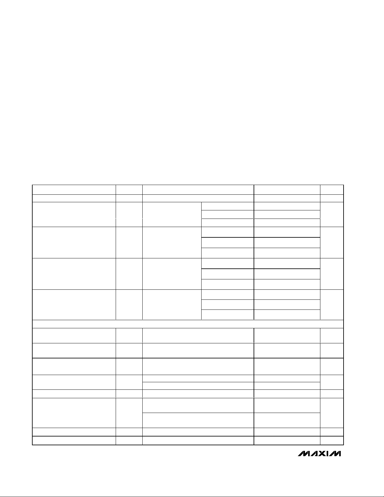
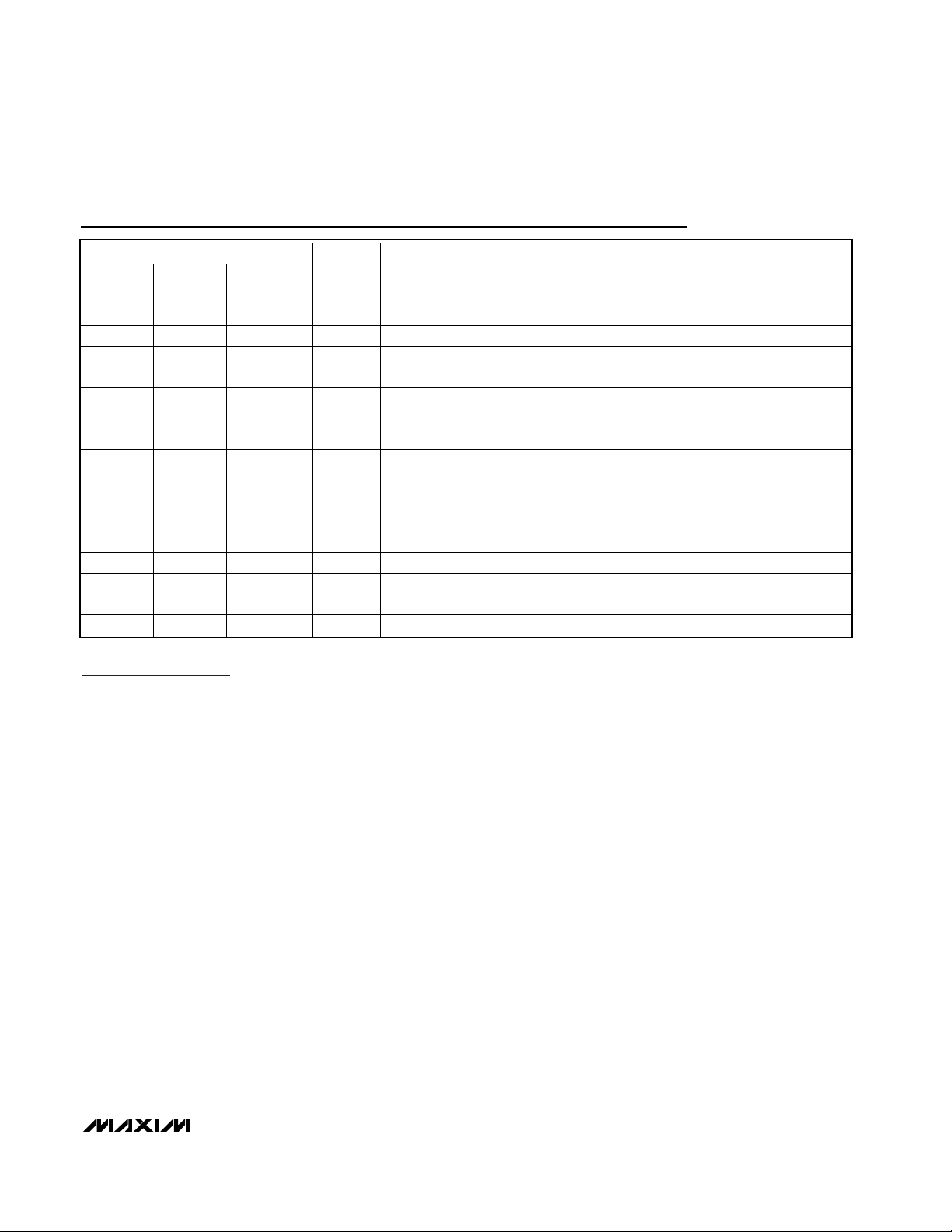
ABSOLUTE MAXIMUM RATINGS
Stresses beyond those listed under “Absolute Maximum Ratings” may cause permanent damage to the device. These are stress ratings only, and functional
operation of the device at these or any other conditions beyond those indicated in the operational sections of the specifications is not implied. Exposure to
absolute maximum rating conditions for extended periods may affect device reliability.
Voltage (with Respect to GND)
V+ .............................................................................-0.3V to +6V
SCL, SDA, AD0, AD1................................................-0.3V to +6V
All Other Pins................................................-0.3V to (V+ + 0.3V)
P4–P31 Current ................................................................±30mA
GND Current .....................................................................800mA
Continuous Power Dissipation
28-Pin PDIP (derate 20.8mW/°C above T
A
= +70°C)1667mW
28-Pin SSOP (derate 9.5mW/°C above TA= +70°C)..762mW
36-Pin SSOP (derate 11.8mW/°C above T
A
= +70°C) ..941mW
40-Pin QFN (derate 26.3mW/°C above T
A
= +70°C) ..2105mW
Operating Temperature Range
(T
MIN
to T
MAX
) ..............................................-40°C to +125°C
Junction Temperature......................................................+150°C
Storage Temperature Range .............................-65°C to +150°C
Lead Temperature (soldering, 10s) .................................+300°C
ELECTRICAL CHARACTERISTICS
(Typical Operating Circuit, V+ = 2.5V to 5.5V, TA= T
MIN
to T
MAX
, unless otherwise noted.) (Note 1)
PARAMETER SYMBOL CONDITIONS MIN TYP MAX UNITS
Operating Supply Voltage V+ 2.5 5.5 V
Shutdown Supply Current I
SHDN
All digital inputs at V+
or GND
All ports programmed
Operating Supply Current I
GPOH
as outputs high, no
load, all other inputs at
V+ or GND
All ports programmed
Operating Supply Current I
GPOL
as outputs low, no
load, all other inputs at
V+ or GND
Al l p or ts p r og r am m ed
Operating Supply Current I
LED
as LE D outp uts, al l LE D s
off, no l oad , al l other
i np uts at V + or GN D T
INPUTS AND OUTPUTS
Logic-High Input Voltage
Port Inputs
Logic-Low Input Voltage
Port Inputs
Input Leakage Current IIH, I
GPIO Input Internal Pullup to V+ I
Hysteresis Voltage GPIO Inputs ∆V
V
IH
V
IL
GPIO inputs without pullup,
IL
V
V+ = 2.5V 12 19 30
PU
V+ = 5.5V 80 120 180
I
GPIO outputs, I
Output High Voltage V
OH
+85°C
GPIO outputs, I
T
Port Sink Current I
Output Short-Circuit Current I
OLSC
V
OL
Port configured output low, shorted to V+ 2.75 11 20 mA
= V+ to GND
PORT
(Note 2)
MAX
= 0.6V 2 10 18 mA
PORT
SOURCE
SOURCE
TA = +25°C 5.5 8
TA = -40°C to +85°C10
T
= T
MIN
to T
MAX
A
11
TA = +25°C 180 230
TA = -40°C to +85°C 250
T
= T
MIN
to T
MAX
A
270
TA = +25°C 170 210
TA = -40°C to +85°C 230
T
= T
MIN
to T
MAX
A
240
TA = +25°C 110 135
TA = -40°C to +85°C 140
= T
MIN
to T
MAX
0.7
✕
A
145
V+
✕
0.3
V+
-100 ±1 +100 nA
0.3 V
= 2mA, TA = -40°C to
V+ -
0.7
= 1mA, TA = T
MIN
to
V+ -
0.7
µA
µA
µA
µA
V
V
µA
V
MAX6956
2-Wire-Interfaced, 2.5V to 5.5V, 20-Port or
28-Port LED Display Driver and I/O Expander
_______________________________________________________________________________________ 3
Note 1: All parameters tested at TA= +25°C. Specifications over temperature are guaranteed by design.
Note 2: Guaranteed by design.
Note 3: A master device must provide a hold time of at least 300ns for the SDA signal (referred to V
IL
of the SCL signal) in order to
bridge the undefined region of SCL’s falling edge.
Note 4: C
b
= total capacitance of one bus line in pF. tRand tFmeasured between 0.3V+ and 0.7V+.
Note 5: I
SINK
≤ 6mA. Cb= total capacitance of one bus line in pF. tRand tFmeasured between 0.3V+ and 0.7V+.
Note 6: Input filters on the SDA and SCL inputs suppress noise spikes less than 50ns.
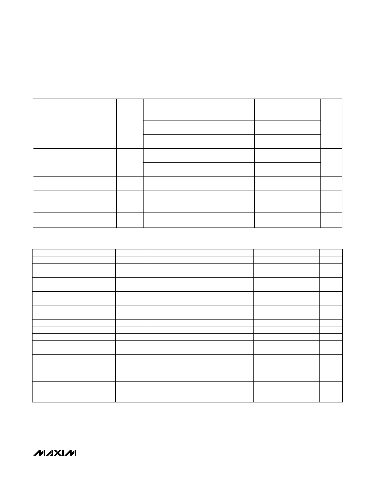
ELECTRICAL CHARACTERISTICS (continued)
(Typical Operating Circuit, V+ = 2.5V to 5.5V, TA= T
MIN
to T
MAX
, unless otherwise noted.) (Note 1)
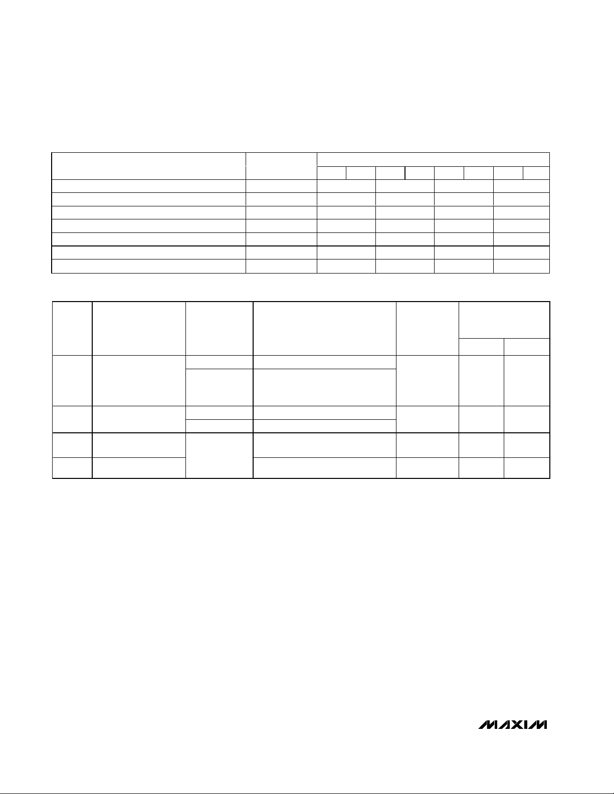
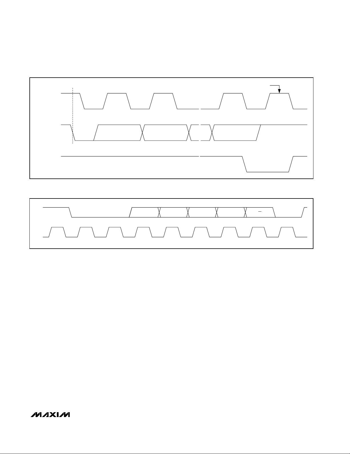
TIMING CHARACTERISTICS (Figure 2)
(V+ = 2.5V to 5.5V, TA= T
MIN
to T
MAX
, unless otherwise noted.) (Note 1)
Port Drive LED Sink Current,
Port Configured as LED Driver
Port Drive Logic Sink Current,
Port Configured as LED Driver
Input High-Voltage SDA, SCL,
AD0, AD1
Input Low-Voltage SDA, SCL,
AD0, AD1
Input Leakage Current SDA, SCL IIH, I
PARAMETER SYMBOL CONDITIONS MIN TYP MAX UNITS
I
DIGIT
I
DIGIT_SC
V
IH
V
IL
IL
Input Capacitance (Note 2) 10 pF
Output Low-Voltage SDA V
OLISINK
V+ = 2.5V, V
current
V+ = 3.3V, V
current (Note 2)
V+ = 5.5V, V
current
V+ = 2.5V, V
current
V+ = 5.5V, V
current
= 2.3V at maximum LED
LED
= 2.4V at maximum LED
LED
= 2.4V at maximum LED
LED
= 0.6V at maximum sink
OUT
= 0.6V at maximum sink
OUT
9.5 13.5 18
18.5 24 27.5
19 25 30
18.5 23 28
19 24 28
✕
0.7
V+
0.3
-50 50 nA
= 6mA 0.4 V
✕
V+
PARAMETER SYMBOL CONDITIONS MIN TYP MAX UNITS
Serial Clock Frequency f
Bus Free Time Between a STOP
and a START Condition
Hold Time (Repeated) START
Condition
Repeated START Condition
Setup Time
STOP Condition Setup Time t
Data Hold Time t
Data Setup Time t
SCL Clock Low Period t
SCL Clock High Period t
Rise Time of Both SDA and SCL
Signals, Receiving
Fall Time of Both SDA and SCL
Signals, Receiving
Fall Time of SDA Transmitting t
Pulse Width of Spike Suppressed t
Capacitive Load for Each Bus
Line
SCL
t
BUF
t
HD, STA
t
SU, STA
SU, STO
HD, DAT
SU, DAT
LOW
HIGH
t
t
,TX
F
SP
C
(Note 3) 15 900 ns
(Notes 2, 4)
R
(Notes 2, 4)
F
(Notes 2, 5)
(Notes 2, 6) 0 50 ns
(Note 2) 400 pF
b
400 kHz
1.3 µs
0.6 µs
0.6 µs
0.6 µs
100 ns
1.3 µs
0.7 µs
20 +
0.1C
20 +
0.1C
20 +
0.1C
b
b
b
300 ns
300 ns
250 ns
mA
mA
V
V
MAX6956
2-Wire-Interfaced, 2.5V to 5.5V, 20-Port or
28-Port LED Display Driver and I/O Expander
4 _______________________________________________________________________________________
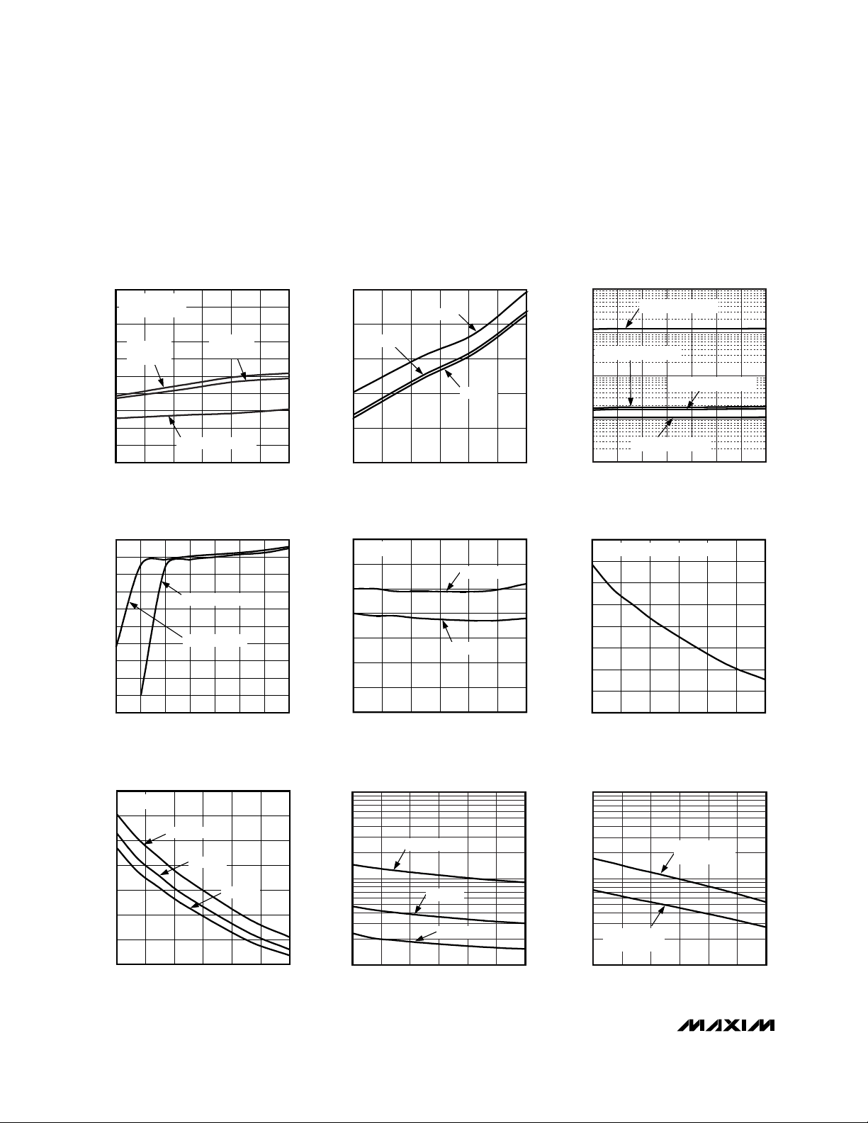
__________________________________________Typical Operating Characteristics
(R
ISET
= 39kΩ, TA = +25°C, unless otherwise noted.)
OPERATING SUPPLY CURRENT
vs. TEMPERATURE
0.40
V+ = 2.5V TO 5.5V
0.36
NO LOAD
0.32
0.28
ALL PORTS
OUTPUT (1)
0.24
0.20
0.16
0.12
SUPPLY CURRENT (mA)
0.08
0.04
0
-40.0 125.0
ALL PORTS LED (OFF)
TEMPERATURE (°C)
LED DRIVER SINK CURRENT
26
24
22
20
18
16
14
12
PORT SINK CURRENT (mA)
10
8
6
2.0 5.5
ALL PORTS
OUTPUT (0)
vs. V+
LED DROP = 2.4V
LED DROP = 1.8V
V+ (V)
SHUTDOWN SUPPLY CURRENT
vs. TEMPERATURE
8
MAX6956 toc01
97.570.042.515.0-12.5
7
V+ = 3.3V
6
5
SUPPLY CURRENT (µA)
4
3
-40.0 125.0
V+ = 5.5V
V+ = 2.5V
TEMPERATURE (°C)
MAX6956 toc02
97.570.042.515.0-12.5
LED DRIVER SINK CURRENT
vs. TEMPERATURE
27
V
= 2.4V
LED
26
MAX6956 toc04
25
24
23
22
PORT SINK CURRENT (mA)
21
20
5.04.53.5 4.03.02.5
-40.0 125.0
TEMPERATURE (°C)
V+ = 5.5V
V+ = 3.3V
MAX6956 toc05
97.570.042.515.0-12.5
OPERATING SUPPLY CURRENT vs. V+
(NO LOADS)
100
ALL PORTS LED (ON)
10
ALL PORTS OUTPUT (1)
1
SUPPLY CURRENT (mA)
0.1
0.01
2.0 5.5
ALL PORTS OUTPUT (0)
ALL PORTS LED (OFF)
V+ (V)
GPO SINK CURRENT vs. TEMPERATURE
(OUTPUT = 0)
18
V+ = 2.5V TO 5.5V, V
16
14
12
10
8
PORT SINK CURRENT (mA)
6
4
2
-40.0 125.0
= 0.6V
PORT
TEMPERATURE (°C)
MAX6956 toc03
5.04.54.03.53.02.5
MAX6956 toc06
97.570.0-12.5 15.0 42.5
GPO SOURCE CURRENT vs. TEMPERATURE
(OUTPUT = 1)
9
V
= 1.4V
PORT
8
7
6
5
4
PORT SOURCE CURRENT (mA)
3
2
-40.0 125.0
V+ = 5.5V
V+ = 3.3V
V+ = 2.5V
TEMPERATURE (°C)
1000
MAX6956 toc07
100
PULLUP CURRENT (µA)
97.570.042.515.0-12.5
10
-40.0 125.0
GPI PULLUP CURRENT
vs. TEMPERATURE
V+ = 5.5V
V+ = 3.3V
V+ = 2.5V
TEMPERATURE (°C)
GPO SHORT-CIRCUIT CURRENT
vs. TEMPERATURE
100
MAX6956 toc08
10
PORT CURRENT (mA)
GPO = 1, PORT
SHORTED TO GND
97.570.042.515.0-12.5
1
-40.0 125.0
TEMPERATURE (°C)
GPO = 0, PORT
SHORTED TO V+
MAX6956 toc09
97.570.042.515.0-12.5
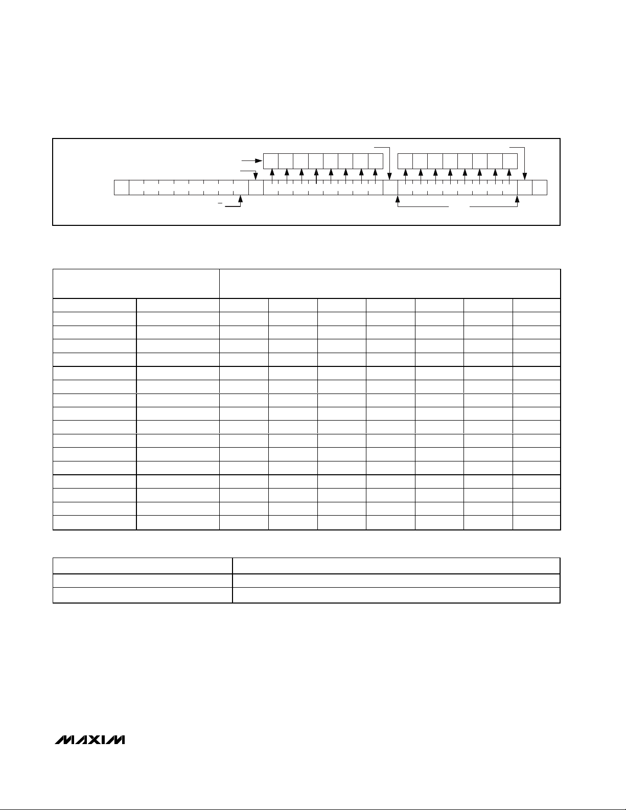
Detailed Description
The MAX6956 LED driver/GPIO peripheral provides up
to 28 I/O ports, P4 to P31, controlled through an I2C-compatible serial interface. The ports can be configured to
any combination of constant-current LED drivers, logic
inputs and logic outputs, and default to logic inputs on
power-up. When fully configured as an LED driver, the
MAX6956 controls up to 28 LED segments with individual 16-step adjustment of the constant current through
each LED segment. A single resistor sets the maximum
segment current for all segments, with a maximum of
24mA per segment. The MAX6956 drives any combination of discrete LEDs and CA digits, including sevensegment and starburst alphanumeric types.
Figure 1 is the MAX6956 functional diagram. Any I/O
port can be configured as a push-pull output (sinking
10mA, sourcing 4.5mA), or a Schmitt-trigger logic
input. Each input has an individually selectable internal
pullup resistor. Additionally, transition detection allows
seven ports (P24 through P30) to be monitored in any
maskable combination for changes in their logic status.
A detected transition is flagged through a status register bit, as well as an interrupt pin (port P31), if desired.
The Typical Operating Circuit shows two MAX6956s
working together controlling three monocolor 16-seg-
ment-plus-DP displays, with five ports left available for
GPIO (P26–P31 of U2).
The port configuration registers set the 28 ports, P4 to
P31, individually as either LED drivers or GPIO. A pair
of bits in registers 0x09 through 0x0F sets each port’s
configuration (Tables 1 and 2).
The 36-pin MAX6956AAX has 28 ports, P4 to P31. The
28-pin MAX6956ANI and MAX6956AAI make only 20
ports available, P12 to P31. The eight unused ports
should be configured as outputs on power-up by writing 0x55 to registers 0x09 and 0x0A. If this is not done,
the eight unused ports remain as floating inputs and
quiescent supply current rises, although there is no
damage to the part.
Register Control of I/O Ports and LEDs
Across Multiple Drivers
The MAX6956 offers 20 or 28 I/O ports, depending on
package choice. These can be applied to a variety of
combinations of different display types, for example:
seven, 7-segment digits (Figure 7). This example
requires two MAX6956s, with one digit being driven by
both devices, half by one MAX6956, half by the other
(digit 4 in this example). The two drivers are static, and
therefore do not need to be synchronized. The
MAX6956 sees CA digits as multiple discrete LEDs. To
MAX6956
2-Wire-Interfaced, 2.5V to 5.5V, 20-Port or
28-Port LED Display Driver and I/O Expander
_______________________________________________________________________________________ 5
Pin Description
PIN
SSOP/DI
1 1 36 ISET
2, 3 2, 3 37, 38, 39 GND Ground
4 4 40 AD0
5–24 ——P 12–P 31
— 5–32
——11, 20, 31 N.C. No Connection
25 33 32 SDA I2C-Compatible Serial Data I/O
26 34 33 SCL I2C-Compatible Serial Clock Input
27 35 34 AD1
28 36 35 V+ Positive Supply Voltage. Bypass V+ to GND with minimum 0.047µF capacitor.
SSOP T H I N Q F N
1–10, 12–19,
21–30
NAME FUNCTION
Segment Current Setting. Connect ISET to GND through a resistor (R
set the maximum segment current.
Address Input 0. Sets device slave address. Connect to either GND, V+, SCL,
SDA to give four logic combinations. See Table 3.
LED Segment Drivers and GPIO. P12 to P31 can be configured as CA LED
drivers, GPIO outputs, CMOS logic inputs, or CMOS logic inputs with weak
pullup resistor.
LED Segment Drivers and GPIO. P4 to P31 can be configured as CA LED
P4–P31
drivers, GPIO outputs, CMOS logic inputs, or CMOS logic inputs with weak
pullup resistor.
Address Input 1. Sets device slave address. Connect to either GND, V+, SCL,
SDA to give four logic combinations. See Table 3.
ISET
) to
MAX6956
simplify access to displays that overlap two MAX6956s,
the MAX6956 provides four virtual ports, P0 through P3.
To update an overlapping digit, send the same code
twice as an eight-port write, once to P28 through P35 of
the first driver, and again to P0 through P7 of the second driver. The first driver ignores the last 4 bits and
the second driver ignores the first 4 bits.
Two addressing methods are available. Any single port
(bit) can be written (set/cleared) at once; or, any
sequence of eight ports can be written (set/cleared) in
any combination at once. There are no boundaries; it is
equally acceptable to write P0 through P7, P1 through
P8, or P31 through P38 (P32 through P38 are nonexistent, so the instructions to these bits are ignored).
Using 8-bit control, a seven-segment digit with a decimal point can be updated in a single byte-write, a 14-
segment digit with DP can be updated in two bytewrites, and 16-segment digits with DP can be updated
in two byte-writes plus a bit write. Also, discrete LEDs
and GPIO port bits can be lit and controlled individually
without affecting other ports.
Shutdown
When the MAX6956 is in shutdown mode, all ports are
forced to inputs (which an be read), and the pullup current sources are turned off. Data in the port and control
registers remain unaltered, so port configuration and
output levels are restored when the MAX6956 is taken
out of shutdown. The display driver can still be programmed while in shutdown mode. For minimum supply current in shutdown mode, logic inputs should be at
GND or V+ potential. Shutdown mode is exited by setting the S bit in the configuration register (Table 8).
2-Wire-Interfaced, 2.5V to 5.5V, 20-Port or
28-Port LED Display Driver and I/O Expander
6 _______________________________________________________________________________________
Table 1. Port Configuration Map
Table 2. Port Configuration Matrix
Note: The logic is inverted between the two output modes; a high makes the output go low in LED segment driver mode (0x00) to
turn that segment on; in GPIO output mode (0x01), a high makes the output go high.
(
)
(
)
REGISTER
Port Configuration for P7, P6, P5, P4 0x09 P7 P6 P5 P4
Port Configuration for P11, P10, P9, P8 0x0A P11 P10 P9 P8
Port Configuration for P15, P14, P13, P12 0x0B P15 P14 P13 P12
Port Configuration for P19, P18, P17, P16 0x0C P19 P18 P17 P16
Port Configuration for P23, P22, P21, P20 0x0D P23 P22 P21 P20
Port Configuration for P27, P26, P25, P24 0x0E P27 P26 P25 P24
Port Configuration for P31, P30, P29, P28 0x0F P31 P30 P29 P28
ADDRESS
CODE (HEX)
D7 D6 D5 D4 D3 D2 D1 D0
REGISTER DATA
MODE FUNCTION
Output LED Segment Driver
Output GPIO Output
Input
Input GPIO Input with Pullup
GPIO Input
Without Pullup
PORT
REGISTER
0x20–0x5F
Register bit = 0 High impedance
Open-drain current sink, with sink
Register bit = 1
Register bit = 0 Active-low logic output
Register bit = 1 Active-high logic output
Register bit =
input logic level
current (up to 24mA) determined
by the appropriate current register
Schmitt logic input 0x09 to 0x0F 1 0
Schmitt logic input with pullup 0x09 to 0x0F 1 1
PIN BEHAVIOR
ADDRESS
CODE
HEX
0x09 to 0x0F 0 0
0x09 to 0x0F 0 1
CONFIGURATION
UPPER LOWER
PORT
BIT PAIR
Shutdown mode is temporarily overridden by the display test function.
Serial Interface
Serial Addressing
The MAX6956 operates as a slave that sends and
receives data through an I2C-compatible 2-wire interface. The interface uses a serial data line (SDA) and a
serial clock line (SCL) to achieve bidirectional communication between master(s) and slave(s). A master (typically a microcontroller) initiates all data transfers to and
from the MAX6956, and generates the SCL clock that
synchronizes the data transfer (Figure 2).
The MAX6956 SDA line operates as both an input and
an open-drain output. A pullup resistor, typically 4.7kΩ,
is required on SDA. The MAX6956 SCL line operates
only as an input. A pullup resistor, typically 4.7kΩ, is
required on SCL if there are multiple masters on the 2wire interface, or if the master in a single-master system
has an open-drain SCL output.
Each transmission consists of a START condition
(Figure 3) sent by a master, followed by the MAX6956
7-bit slave address plus R/W bit (Figure 6), a register
address byte, one or more data bytes, and finally a
STOP condition (Figure 3).
Start and Stop Conditions
Both SCL and SDA remain high when the interface is
not busy. A master signals the beginning of a transmission with a START (S) condition by transitioning SDA
from high to low while SCL is high. When the master
MAX6956
2-Wire-Interfaced, 2.5V to 5.5V, 20-Port or
28-Port LED Display Driver and I/O Expander
_______________________________________________________________________________________________________ 7
Figure 1. MAX6956 Functional Diagram
INTENSITY REGISTERS
TEST REGISTER
PORT REGISTERS
MASK REGISTER
CONFIGURATION
REGISTERS
R/W
CEDATA
8
MAX6956
P4 TO P31
LED DRIVERS
OR GPIO
LED DRIVERS AND GPIO
SEGMENT OR
GPIO DATA
8
INTENSITY
TEST
CONFIGURATION
R/W
PORT CHANGE
DETECTOR
AD0
AD1
SDA
SCL
ADDRESS
MATCHER
7
D0 D1 D2 D3 D4 D5 D6 D7 D8 D9 D10 D11 D12 D13 D14 D15
7
SLAVE ADDRESS BYTE
8
DATA BYTE COMMAND BYTE
R/W7-BIT DEVICE ADDRESS
COMMAND
REGISTER DECODE
8
TO/FROM DATA REGISTERS
TO COMMAND REGISTERS
COMMAND BYTEDATA BYTE
MAX6956
has finished communicating with the slave, it issues a
STOP (P) condition by transitioning SDA from low to
high while SCL is high. The bus is then free for another
transmission (Figure 3).
Bit Transfer
One data bit is transferred during each clock pulse.
The data on SDA must remain stable while SCL is high
(Figure 4).
Acknowledge
The acknowledge bit is a clocked 9th bit, which the
recipient uses to handshake receipt of each byte of
data (Figure 5). Thus, each byte transferred effectively
requires 9 bits. The master generates the 9th clock
pulse, and the recipient pulls down SDA during the
acknowledge clock pulse, such that the SDA line is stable low during the high period of the clock pulse. When
the master is transmitting to the MAX6956, the
MAX6956 generates the acknowledge bit because the
2-Wire-Interfaced, 2.5V to 5.5V, 20-Port or
28-Port LED Display Driver and I/O Expander
8 _______________________________________________________________________________________
Figure 2. 2-Wire Serial Interface Timing Details
Figure 3. Standard Stop Conditions
Figure 4. Bit Transfer
SDA
t
BUF
SCL
t
SU, DAT
t
LOW
t
HD, DAT
t
SU, STA
t
HD, STA
t
SU, STO
t
HD, STA
START CONDITION
t
HIGH
t
R
SDA
SCL
S
START
CONDITION
SDA
t
F
REPEATED START CONDITION
P
STOP
CONDITION
START CONDITIONSTOP CONDITION
SCL
DATA LINE STABLE;
DATA VALID
CHANGE OF DATA ALLOWED
MAX6956 is the recipient. When the MAX6956 is transmitting to the master, the master generates the
acknowledge bit because the master is the recipient.
Slave Address
The MAX6956 has a 7-bit-long slave address (Figure 6).
The eighth bit following the 7-bit slave address is the
R/W bit. It is low for a write command, high for a read
command.
The first 3 bits (MSBs) of the MAX6956 slave address
are always 100. Slave address bits A3, A2, A1, and A0
are selected by address inputs, AD1 and AD0. These
two input pins may be connected to GND, V+, SDA, or
SCL. The MAX6956 has 16 possible slave addresses
(Table 3) and therefore, a maximum of 16 MAX6956
devices may share the same interface.
Message Format for Writing
the MAX6956
A write to the MAX6956 comprises the transmission of
the MAX6956’s slave address with the R/ W bit set to
zero, followed by at least 1 byte of information. The first
byte of information is the command byte. The command byte determines which register of the MAX6956
is to be written by the next byte, if received. If a STOP
condition is detected after the command byte is
received, then the MAX6956 takes no further action
(Figure 8) beyond storing the command byte.
Any bytes received after the command byte are data
bytes. The first data byte goes into the internal register of
the MAX6956 selected by the command byte (Figure 9). If
multiple data bytes are transmitted before a STOP condition is detected, these bytes are generally stored in subsequent MAX6956 internal registers because the command
byte address generally autoincrements (Table 4).
Message Format for Reading
The MAX6956 is read using the MAX6956’s internally
stored command byte as address pointer, the same
way the stored command byte is used as address
pointer for a write. The pointer generally autoincrements after each data byte is read using the same rules
as for a write (Table 4). Thus, a read is initiated by first
configuring the MAX6956’s command byte by perform-
MAX6956
2-Wire-Interfaced, 2.5V to 5.5V, 20-Port or
28-Port LED Display Driver and I/O Expander
_______________________________________________________________________________________ 9
Figure 5. Acknowledge
Figure 6. Slave Address
START CONDITION
SCL
BY TRANSMITTER
SDA
SCL
SDA
S
SDA
BY RECEIVER
1 0 A3 A2 A1 A00
MSB
CLOCK PULSE FOR ACKNOWLEDGMENT
12 89
R/W
LSB
ACK

MAX6956
2-Wire-Interfaced, 2.5V to 5.5V, 20-Port or
28-Port LED Display Driver and I/O Expander
10 ______________________________________________________________________________________
Figure 7. Two MAX6956s Controlling Seven 7-Segment Displays
Figure 8. Command Byte Received
Figure 9. Command and Single Data Byte Received
7-SEGMENT DIGIT 1
7-SEGMENT DIGIT 2 7-SEGMENT DIGIT 3 7-SEGMENT DIGIT 4
VIRTUAL SEGMENTS
P0 P1 P2 P3 P4 P5 P6 P7 P8 P9 P10 P11 P12 P13 P14 P15 P16 P17 P18 P19 P20 P21 P22 P23 P24 P25 P26 P27 P28 P29 P30 P31
7-SEGMENT DIGIT 5 7-SEGMENT DIGIT 6 7-SEGMENT DIGIT 7
VIRTUAL SEGMENTS
P0 P1 P2 P3 P4 P5 P6 P7 P8 P9 P10 P11 P12 P13 P14 P15 P16 P17 P18 P19 P20 P21 P22 P23 P24 P25 P26 P27 P28 P29 P30 P31
V+
V+
COMMAND BYTE IS STORED ON RECEIPT OF STOP CONDITION
ACKNOWLEDGE FROM MAX6956
SAAP0
COMMAND BYTE RECEIVED
SLAVE ADDRESS
R/W
D15 D14 D13 D12 D11 D10 D9 D8
COMMAND BYTE
ACKNOWLEDGE FROM MAX6956
ACKNOWLEDGE FROM MAX6956 ACKNOWLEDGE FROM MAX6956
HOW COMMAND BYTE AND DATA BYTE MAP INTO MAX6956's REGISTER
SAAAP0
ACKNOWLEDGE FROM MAX6956
SLAVE ADDRESS
R/W
D15 D14 D13 D12 D11 D10 D9 D8 D1 D0D3 D2D5 D4D7 D6
COMMAND BYTE
DATA BYTE
1 BYTE
ing a write (Figure 8). The master can now read n consecutive bytes from the MAX6956, with the first data
byte being read from the register addressed by the initialized command byte. When performing read-afterwrite verification, remember to reset the command
byte’s address because the stored control byte
address generally has been autoincremented after the
write (Table 4). Table 5 is the register address map.
Operation with Multiple Masters
If the MAX6956 is operated on a 2-wire interface with
multiple masters, a master reading the MAX6956
should use a repeated start between the write, which
sets the MAX6956’s address pointer, and the read(s)
that takes the data from the location(s). This is because
it is possible for master 2 to take over the bus after
master 1 has set up the MAX6956’s address pointer but
before master 1 has read the data. If master 2 subse-
MAX6956
2-Wire-Interfaced, 2.5V to 5.5V, 20-Port or
28-Port LED Display Driver and I/O Expander
______________________________________________________________________________________ 11
Figure 10. n Data Bytes Received
Table 3. MAX6956 Address Map
Table 4. Autoincrement Rules
HOW COMMAND BYTE AND DATA BYTE MAP INTO MAX6956's REGISTER
ACKNOWLEDGE FROM MAX6956
SA AAP0
AD1 AD0 A6 A5 A4 A3 A2 A1 A0
GND GND 1 0 0 0 0 0 0
GND V+ 1000001
GND SDA 1000010
GND SCL 1000011
V+ GND 1000100
V+ V+ 1000101
V+ SDA 1000110
V+ SCL 1000111
SDA GND 1001000
SDA V+ 1001001
SDA SDA 1 0 0 1 0 1 0
SDA SCL 1 0 0 1 0 1 1
SCL GND 1001100
SCL V+ 1001101
SCL SDA 1 0 0 1 1 1 0
SCL SCL 1 0 0 1 1 1 1
PIN
CONNECTION
SLAVE ADDRESS
R/W
ACKNOWLEDGE FROM MAX6956
D15 D14 D13 D12 D11 D10 D9 D8 D1 D0D3 D2D5 D4D7 D6
COMMAND BYTE
AUTOINCREMENT MEMORY WORD ADDRESS
DEVICE ADDRESS
ACKNOWLEDGE FROM MAX6956
DATA BYTE
n BYTES
COMMAND BYTE ADDRESS RANGE AUTOINCREMENT BEHAVIOR
x0000000 to x1111110 Command address autoincrements after byte read or written
x1111111 Command address remains at x1111111 after byte written or read

MAX6956
2-Wire-Interfaced, 2.5V to 5.5V, 20-Port or
28-Port LED Display Driver and I/O Expander
12 ______________________________________________________________________________________
Table 5. Register Address Map
REGISTER
No-Op X 0 0 0 0 0 0 0 0x00
Global Current X 0 0 0 0 0 1 0 0x02
Configuration X 0 0 0 0 1 0 0 0x04
Transition Detect Mask X 0 0 0 0 1 1 0 0x06
Display Test X 0 0 0 0 1 1 1 0x07
Port Configuration P7, P6, P5, P4 X 0 0 0 1 0 0 1 0x09
Port Configuration P11, P10, P9, P8 X 0 0 0 1 0 1 0 0x0A
Port Configuration P15, P14, P13, P12 X 0 0 0 1 0 1 1 0x0B
Port Configuration P19, P18, P17, P16 X 0 0 0 1 1 0 0 0x0C
Port Configuration P23, P22, P21, P20 X 0 0 0 1 1 0 1 0x0D
Port Configuration P27, P26, P25, P24 X 0 0 0 1 1 1 0 0x0E
Port Configuration P31, P30, P29, P28 X 0 0 0 1 1 1 1 0x0F
Current054
Current076
Current098 X 0 0 1 0 1 0 0 0x14
Current0BA X 0 0 1 0 1 0 1 0x15
Current0DC X 0 0 1 0 1 1 0 0x16
Current0FE X 0 0 1 0 1 1 1 0x17
Current110 X 0 0 1 1 0 0 0 0x18
Current132 X 0 0 1 1 0 0 1 0x19
Current154 X 0 0 1 1 0 1 0 0x1A
Current176 X 0 0 1 1 0 1 1 0x1B
Current198 X 0 0 1 1 1 0 0 0x1C
Current1BA X 0 0 1 1 1 0 1 0x1D
Current1DC X 0 0 1 1 1 1 0 0x1E
Current1FE X 0 0 1 1 1 1 1 0x1F
Port 0 only (virtual port, no action) X 0 1 0 0 0 0 0 0x20
Port 1 only (virtual port, no action) X 0 1 0 0 0 0 1 0x21
Port 2 only (virtual port, no action) X 0 1 0 0 0 1 0 0x22
Port 3 only (virtual port, no action) X 0 1 0 0 0 1 1 0x23
Port 4 only (data bit D0; D7–D1 read as 0) X 0 1 0 0 1 0 0 0x24
Port 5 only (data bit D0; D7–D1 read as 0) X 0 1 0 0 1 0 1 0x25
Port 6 only (data bit D0; D7–D1 read as 0) X 0 1 0 0 1 1 0 0x26
Port 7 only (data bit D0; D7–D1 read as 0) X 0 1 0 0 1 1 1 0x27
Port 8 only (data bit D0; D7–D1 read as 0) X 0 1 0 1 0 0 0 0x28
Port 9 only (data bit D0; D7–D1 read as 0) X 0 1 0 1 0 0 1 0x29
Port 10 only (data bit D0; D7–D1 read as 0) X 0 1 0 1 0 1 0 0x2A
D15 D14 D13 D12 D11 D10 D9 D8
X 0 0 1 0 0 1 0 0x12
X 0 0 1 0 0 1 1 0x13
COMMAND ADDRESS
HEX
CODE

MAX6956
2-Wire-Interfaced, 2.5V to 5.5V, 20-Port or
28-Port LED Display Driver and I/O Expander
______________________________________________________________________________________ 13
Table 5. Register Address Map (continued)
REGISTER
Port 11 only (data bit D0; D7–D1 read as 0) X 0 1 0 1 0 1 1 0x2B
Port 12 only (data bit D0; D7–D1 read as 0) X 0 1 0 1 1 0 0 0x2C
Port 13 only (data bit D0; D7–D1 read as 0) X 0 1 0 1 1 0 1 0x2D
Port 14 only (data bit D0; D7–D1 read as 0) X 0 1 0 1 1 1 0 0x2E
Port 15 only (data bit D0; D7–D1 read as 0) X 0 1 0 1 1 1 1 0x2F
Port 16 only (data bit D0; D7–D1 read as 0) X 0 1 1 0 0 0 0 0x30
Port 17 only (data bit D0; D7–D1 read as 0) X 0 1 1 0 0 0 1 0x31
Port 18 only (data bit D0; D7–D1 read as 0) X 0 1 1 0 0 1 0 0x32
Port 19 only (data bit D0; D7–D1 read as 0) X 0 1 1 0 0 1 1 0x33
Port 20 only (data bit D0; D7–D1 read as 0) X 0 1 1 0 1 0 0 0x34
Port 21 only (data bit D0; D7–D1 read as 0) X 0 1 1 0 1 0 1 0x35
Port 22 only (data bit D0; D7–D1 read as 0) X 0 1 1 0 1 1 0 0x36
Port 23 only (data bit D0; D7–D1 read as 0) X 0 1 1 0 1 1 1 0x37
Port 24 only (data bit D0; D7–D1 read as 0) X 0 1 1 1 0 0 0 0x38
Port 25 only (data bit D0; D7–D1 read as 0) X 0 1 1 1 0 0 1 0x39
Port 26 only (data bit D0; D7–D1 read as 0) X 0 1 1 1 0 1 0 0x3A
Port 27 only (data bit D0; D7–D1 read as 0) X 0 1 1 1 0 1 1 0x3B
Port 28 only (data bit D0; D7–D1 read as 0) X 0 1 1 1 1 0 0 0x3C
Port 29 only (data bit D0; D7–D1 read as 0) X 0 1 1 1 1 0 1 0x3D
Port 30 only (data bit D0; D7–D1 read as 0) X 0 1 1 1 1 1 0 0x3E
Port 31 only (data bit D0; D7–D1 read as 0) X 0 1 1 1 1 1 1 0x3F
4 ports 4–7 (data bits D0–D3; D4–D7 read as 0) X 1 0 0 0 0 0 0 0x40
5 ports 4–8 (data bits D0–D4; D5–D7 read as 0) X 1 0 0 0 0 0 1 0x41
6 ports 4–9 (data bits D0–D5; D6–D7 read as 0) X 1 0 0 0 0 1 0 0x42
7 ports 4–10 (data bits D0–D6; D7 reads as 0) X 1 0 0 0 0 1 1 0x43
8 ports 4–11 (data bits D0–D7) X 1 0 0 0 1 0 0 0x44
8 ports 5–12 (data bits D0–D7) X 1 0 0 0 1 0 1 0x45
8 ports 6–13 (data bits D0–D7) X 1 0 0 0 1 1 0 0x46
8 ports 7–14 (data bits D0–D7) X 1 0 0 0 1 1 1 0x47
8 ports 8–15 (data bits D0–D7) X 1 0 0 1 0 0 0 0x48
8 ports 9–16 (data bits D0–D7) X 1 0 0 1 0 0 1 0x49
8 ports 10–17 (data bits D0–D7) X 1 0 0 1 0 1 0 0x4A
8 ports 11–18 (data bits D0–D7) X 1 0 0 1 0 1 1 0x4B
8 ports 12–19 (data bits D0–D7) X 1 0 0 1 1 0 0 0x4C
8 ports 13–20 (data bits D0–D7) X 1 0 0 1 1 0 1 0x4D
8 ports 14–21 (data bits D0–D7) X 1 0 0 1 1 1 0 0x4E
8 ports 15–22 (data bits D0–D7) X 1 0 0 1 1 1 1 0x4F
D15 D14 D13 D12 D11 D10 D9 D8
COMMAND ADDRESS
HEX
CODE

MAX6956
quently changes, the MAX6956’s address pointer, then
master 1’s delayed read may be from an unexpected
location.
Command Address Autoincrementing
Address autoincrementing allows the MAX6956 to be
configured with the shortest number of transmissions
by minimizing the number of times the command
address needs to be sent. The command address
stored in the MAX6956 generally increments after each
data byte is written or read (Table 4).
Initial Power-Up
On initial power-up, all control registers are reset, the
current registers are set to minimum value, and the
MAX6956 enters shutdown mode (Table 6).
LED Current Control
LED segment drive current can be set either globally or
individually. Global control simplifies the operation
when all LEDs are set to the same current level,
because writing just the global current register sets the
current for all ports configured as LED segment drivers.
It is also possible to individually control the current
drive of each LED segment driver. Individual/global
brightness control is selected by setting the configuration register I bit (Table 9). The global current register
(0x02) data are then ignored, and segment currents are
set using register addresses 0x12 through 0x1F (Tables
12, 13, and 14). Each segment is controlled by a nibble
of one of the 16 current registers.
Transition (Port Data Change) Detection
Port transition detection allows any combination of the
seven ports P24–P30 to be continuously monitored for
changes in their logic status (Figure 11). A detected
change is flagged on the transition detection mask register INT status bit, D7 (Table 15). If port P31 is configured as an output (Tables 1 and 2), then P31 also
automatically becomes an active-high interrupt output
(INT), which follows the condition of the INT status bit.
Port P31 is set as output by writing bit D7 = 0 and bit
D6 = 1 to the port configuration register (Table 1). Note
that the MAX6956 does not identify which specific
port(s) caused the interrupt, but provides an alert that
one or more port levels have changed.
2-Wire-Interfaced, 2.5V to 5.5V, 20-Port or
28-Port LED Display Driver and I/O Expander
14 ______________________________________________________________________________________
Table 5. Register Address Map (continued)
Note: Unused bits read as 0.
REGISTER
8 ports 16–23 (data bits D0–D7) X 1 0 1 0 0 0 0 0x50
8 ports 17–24 (data bits D0–D7) X 1 0 1 0 0 0 1 0x51
8 ports 18–25 (data bits D0–D7) X 1 0 1 0 0 1 0 0x52
8 ports 19–26 (data bits D0–D7) X 1 0 1 0 0 1 1 0x53
8 ports 20–27 (data bits D0–D7) X 1 0 1 0 1 0 0 0x54
8 ports 21–28 (data bits D0–D7) X 1 0 1 0 1 0 1 0x55
8 ports 22–29 (data bits D0–D7) X 1 0 1 0 1 1 0 0x56
8 ports 23–30 (data bits D0–D7) X 1 0 1 0 1 1 1 0x57
8 ports 24–31 (data bits D0–D7) X 1 0 1 1 0 0 0 0x58
7 ports 25–31 (data bits D0–D6; D7 reads as 0) X 1 0 1 1 0 0 1 0x59
6 ports 26–31 (data bits D0–D5; D6–D7 read as 0) X 1 0 1 1 0 1 0 0x5A
5 ports 27–31 (data bits D0–D4; D5–D7 read as 0) X 1 0 1 1 0 1 1 0x5B
4 ports 28–31 (data bits D0–D3; D4–D7 read as 0) X 1 0 1 1 1 0 0 0x5C
3 ports 29–31 (data bits D0–D2; D3–D7 read as 0) X 1 0 1 1 1 0 1 0x5D
2 ports 30–31 (data bits D0–D1; D2–D7 read as 0) X 1 0 1 1 1 1 0 0x5E
1 port 31 only (data bit D0; D1–D7 read as 0) X 1 0 1 1 1 1 1 0x5F
D15 D14 D13 D12 D11 D10 D9 D8
COMMAND ADDRESS
HEX
CODE
MAX6956
2-Wire-Interfaced, 2.5V to 5.5V, 20-Port or
28-Port LED Display Driver and I/O Expander
Table 6. Power-Up Configuration
X = unused bits; if read, zero results.
______________________________________________________________________________________ 15
REGISTER
FUNCTION
Port Register
Bits 4 to 31
Global
Current
Configuration
Register
Input Mask
Register
Display Test Normal Operation 0x07 X X X X X X X 0
Port
Configuration
Port
Configuration
Port
Configuration
Port
Configuration
Port
Configuration
Port
Configuration
Port
Configuration
Current054 1/16 (minimum on) 0x12 0 0 0 0 0 0 0 0
Current076 1/16 (minimum on) 0x13 0 0 0 0 0 0 0 0
Current098 1/16 (minimum on) 0x14 0 0 0 0 0 0 0 0
Current0BA 1/16 (minimum on) 0x15 0 0 0 0 0 0 0 0
Current0DC 1/16 (minimum on) 0x16 0 0 0 0 0 0 0 0
Current0FE 1/16 (minimum on) 0x17 0 0 0 0 0 0 0 0
Current110 1/16 (minimum on) 0x18 0 0 0 0 0 0 0 0
Current132 1/16 (minimum on) 0x19 0 0 0 0 0 0 0 0
Current154 1/16 (minimum on) 0x1A 0 0 0 0 0 0 0 0
Current176 1/16 (minimum on) 0x1B 0 0 0 0 0 0 0 0
Current198 1/16 (minimum on) 0x1C 0 0 0 0 0 0 0 0
Current1BA 1/16 (minimum on) 0x1D 0 0 0 0 0 0 0 0
Current1DC 1/16 (minimum on) 0x1E 0 0 0 0 0 0 0 0
Current1FE 1/16 (minimum on) 0x1F 0 0 0 0 0 0 0 0
P7, P6, P5, P4: GPIO Inputs Without Pullup 0x09 1 0 1 0 1 0 1 0
P11, P10, P9, P8: GPIO Inputs Without Pullup 0x0A 1 0 1 0 1 0 1 0
P15, P14, P13, P12: GPIO Inputs Without Pullup 0x0B 1 0 1 0 1 0 1 0
P19, P18, P17, P16: GPIO Inputs Without Pullup 0x0C 1 0 1 0 1 0 1 0
P23, P22, P21, P20: GPIO Inputs Without Pullup 0x0D 1 0 1 0 1 0 1 0
P27, P26, P25, P24: GPIO Inputs Without Pullup 0x0E 1 0 1 0 1 0 1 0
P31, P30, P29, P28: GPIO Inputs Without Pullup 0x0F 1 0 1 0 1 0 1 0
POWER-UP CONDITION
LED Off; GPIO Output Low
1/16 (minimum on) 0x02 X X X X 0 0 0 0
Shutdown Enabled
Current Control = Global
Transition Detection Disabled
All Clear (Masked Off) 0x06 X 0 0 0 0 0 0 0
ADDRESS
CODE
(HEX)
0x24 to
0x3F
0x04 0 0 X X X X X 0
D7 D6 D5 D4 D3 D2 D1 D0
XXXXXXX0
REGISTER DATA

MAX6956
The mask register contains 7 mask bits, which select
which of the seven ports P24–P30 are to be monitored
(Table 15). Set the appropriate mask bit to enable that
port for transition detect. Clear the mask bit if transitions
on that port are to be ignored. Transition detection
works regardless of whether the port being monitored is
set to input or output, but generally, it is not particularly
useful to enable transition detection for outputs.
To use transition detection, first set up the mask register
and configure port P31 as an output, as described
above. Then enable transition detection by setting the
M bit in the configuration register (Table 10). Whenever
the configuration register is written with the M bit set,
the MAX6956 updates an internal 7-bit snapshot register, which holds the comparison copy of the logic states
of ports P24 through P30. The update action occurs
regardless of the previous state of the M bit, so that it is
not necessary to clear the M bit and then set it again to
update the snapshot register.
When the configuration register is written with the M bit
set, transition detection is enabled and remains
enabled until either the configuration register is written
2-Wire-Interfaced, 2.5V to 5.5V, 20-Port or
28-Port LED Display Driver and I/O Expander
16 ______________________________________________________________________________________
Table 7. Configuration Register Format
Table 8. Shutdown Control (S Data Bit D0) Format
Table 10. Transition Detection Control (M-Data Bit D7) Format
Table 9. Global Current Control (I Data Bit D6) Format
FUNCTION
Configuration Register 0x04 M I XXXXXS
FUNCTION
Shutdown 0x04 M I XXXXX0
Normal Operation 0x04 M I XXXXX1
FUNCTION
Global
Constant-current limits for all digits are
controlled by one setting in the Global Current
register, 0x02
Individual Segment
Constant-current limit for each digit is
individually controlled by the settings in the
Current054 through Current1FE registers
ADDRESS CODE
(HEX)
ADDRESS CODE
(HEX)
D7 D6 D5 D4 D3 D2 D1 D0
D7 D6 D5 D4 D3 D2 D1 D0
ADDRESS
CODE (HEX)
D7 D6 D5 D4 D3 D2 D1 D0
0x04 M 0 XXXXXS
0x04 M 1 XXXXXS
REGISTER DATA
REGISTER DATA
REGISTER DATA
FUNCTION
Disabled 0x04 0 I XXXXXS
Enabled 0x04 1 I XXXXXS
ADDRESS CODE
(HEX)
D7 D6 D5 D4 D3 D2 D1 D0
REGISTER DATA

with the M bit clear, or a transition is detected. The INT
status bit (transition detection mask register bit D7)
goes low. Port P31 (if enabled as INT output) also goes
low, if it was not already low.
Once transition detection is enabled, the MAX6956
continuously compares the snapshot register against
the changing states of P24 through P31. If a change on
any of the monitored ports is detected, even for a short
time (like a pulse), the INT status bit (transition detection mask register bit D7) is set. Port P31 (if enabled as
INT output) also goes high. The INT output and INT status bit are not cleared if more changes occur or if the
data pattern returns to its original snapshot condition.
The only way to clear INT is to access (read or write)
the transition detection mask register (Table 15). So if
the transition detection mask register is read twice in
succession after a transition event, the first time reads
with bit D7 set (identifying the event), and the second
time reads with bit D7 clear.
Transition detection is a one-shot event. When INT has
been cleared after responding to a transition event,
transition detection is automatically disabled, even
though the M bit in the configuration register remains
set (unless cleared by the user). Reenable transition
detection by writing the configuration register with the
M bit set, to take a new snapshot of the seven ports
P24 to P30.
Display Test Register
Display test mode turns on all ports configured as LED
drivers by overriding, but not altering, all controls and
port registers, except the port configuration register
(Table 16). Only ports configured as LED drivers are
affected. Ports configured as GPIO push-pull outputs
do not change state. In display test mode, each port’s
current is temporarily set to 1/2 the maximum current
limit as controlled by R
ISET
.
Selecting External Component R
ISET
to Set Maximum Segment Current
The MAX6956 uses an external resistor R
ISET
to set the
maximum segment current. The recommended value,
39kΩ, sets the maximum current to 24mA, which makes
the segment current adjustable from 1.5mA to 24mA in
1.5mA steps.
To set a different segment current, use the formula:
R
ISET
= 936kΩ / I
SEG
where I
SEG
is the desired maximum segment current.
MAX6956
2-Wire-Interfaced, 2.5V to 5.5V, 20-Port or
28-Port LED Display Driver and I/O Expander
______________________________________________________________________________________ 17
Table 11. Global Segment Current Register Format
X = Don’t care bit.
LED DRIVE
FRACTION
1/16 1.5 0x02 X X X X 0 0 0 0 0xX0
2/16 3 0x02 X X X X 0 0 0 1 0xX1
3/16 4.5 0x02 X X X X 0 0 1 0 0xX2
4/16 6 0x02 X X X X 0 0 1 1 0xX3
5/16 7.5 0x02 X X X X 0 1 0 0 0xX4
6/16 9 0x02 X X X X 0 1 0 1 0xX5
7/16 10.5 0x02 X X X X 0 1 1 0 0xX6
8/16 12 0x02 X X X X 0 1 1 1 0xX7
9/16 13.5 0x02 X X X X 1 0 0 0 0xX8
10/16 15 0x02 X X X X 1 0 0 1 0xX9
11/16 16.5 0x02 X X X X 1 0 1 0 0xXA
12/16 18 0x02 X X X X 1 0 1 1 0xXB
13/16 19.5 0x02 X X X X 1 1 0 0 0xXC
14/16 21 0x02 X X X X 1 1 0 1 0xXD
15/16 22.5 0x02 X X X X 1 1 1 0 0xXE
16/16 24 0x02 X X X X 1 1 1 1 0xXF
TYPICAL SEGMENT
CURRENT (mA)
ADDRESS
CODE (HEX)
D7 D6 D5 D4 D3 D2 D1 D0 HEX CODE
MAX6956
2-Wire-Interfaced, 2.5V to 5.5V, 20-Port or
28-Port LED Display Driver and I/O Expander
18 ______________________________________________________________________________________
Table 12. Individual Segment Current Registers
Table 13. Even Individual Segment Current Format
REGISTER
FUNCTION
Current054 register 0x12 Segment 5 Segment 4
Current076 register 0x13 Segment 7 Segment 6
Current098 register 0x14 Segment 9 Segment 8
Current0BA register 0x15 Segment 11 Segment 10
Current0DC register 0x16 Segment 13 Segment 12
Current0FE register 0x17 Segment 15 Segment 14
Current110 register 0x18 Segment 17 Segment 16
Current132 register 0x19 Segment 19 Segment 18
Current154 register 0x1A Segment 21 Segment 20
Current176 register 0x1B Segment 23 Segment 22
Current198 register 0x1C Segment 25 Segment 24
Current1BA register 0x1D Segment 27 Segment 26
Current1DC register 0x1E Segment 29 Segment 28
Current1FE register 0x1F Segment 31 Segment 30
ADDRESS
CODE (HEX)
D7 D6 D5 D4 D3 D2 D1 D0
LED DRIVE
FRACTION
1/16 1.5 0x12 to 0x1F 0000 0xX0
2/16 3 0x12 to 0x1F 0001 0xX1
3/16 4.5 0x12 to 0x1F 0010 0xX2
4/16 6 0x12 to 0x1F 0011 0xX3
5/16 7.5 0x12 to 0x1F 0100 0xX4
6/16 9 0x12 to 0x1F 0101 0xX5
7/16 10.5 0x12 to 0x1F See Table 14. 0110 0xX6
8/16 12 0x12 to 0x1F 0111 0xX7
9/16 13.5 0x12 to 0x1F 1000 0xX8
10/16 15 0x12 to 0x1F 1001 0xX9
11/16 16.5 0x12 to 0x1F 1010 0xXA
12/16 18 0x12 to 0x1F 1011 0xXB
13/16 19.5 0x12 to 0x1F 1100 0xXC
14/16 21 0x12 to 0x1F 1101 0xXD
15/16 22.5 0x12 to 0x1F 1110 0xXE
16/16 24 0x12 to 0x1F 1111 0xXF
SEGMENT
CONSTANT
CURRENT WITH
R
= 39kΩ (mA)
ISET
ADDRESS
CODE (HEX)
D7 D6 D5 D4 D3 D2 D1 D0 HEX CODE

MAX6956
2-Wire-Interfaced, 2.5V to 5.5V, 20-Port or
28-Port LED Display Driver and I/O Expander
______________________________________________________________________________________ 19
The recommended value of R
ISET
is 39kΩ.
The recommended value of R
ISET
is the minimum
allowed value, since it sets the display driver to the
maximum allowed segment current. R
ISET
can be a
higher value to set the segment current to a lower maximum value where desired. The user must also ensure
that the maximum current specifications of the LEDs
connected to the driver are not exceeded.
The drive current for each segment can be controlled
through programming either the Global Current register
(Table 11) or Individual Segment Current registers
(Tables 12, 13, and 14), according to the setting of the
Current Control bit of the Configuration register (Table 9).
These registers select the LED’s constant-current drive
from 16 equal fractions of the maximum segment current. The current difference between successive current
steps, I
STEP
, is therefore determined by the formula:
I
STEP
= I
SEG
/ 16
If I
SEG
= 24mA, then I
STEP
= 24mA / 16 = 1.5mA.
Applications Information
Driving Bicolor and Tricolor LEDs
Bicolor digits group a red and a green die together for
each display element, so that the element can be lit
red, green (or orange), depending on which die (or
both) is lit. The MAX6956 allows each segment’s current to be set individually from 1/16th (minimum current
and LED intensity) to 16/16th (maximum current and
LED intensity), as well as off (zero current). Thus, a
bicolor (red-green) segment pair can be set to 289
color/intensity combinations. A discrete or CA tricolor
(red-green-yellow or red-green-blue) segment triad can
be set to 4913 color/intensity combinations.
Power Dissipation Issues
Each MAX6956 port can sink a current of 24mA into an
LED with a 2.4V forward-voltage drop when operated
from a supply voltage of at least 3.0V. The minimum
voltage drop across the internal LED drivers is therefore (3.0V - 2.4V) = 0.6V. The MAX6956 can sink 28 x
24mA = 672mA when all outputs are operating as LED
Table 14. Odd Individual Segment Current Format
LED
DRIVE
FRACTION
1/16 1.5 0x12 to 0x1F 0 0 0 0 0x0X
2/16 3 0x12 to 0x1F 0 0 0 1 0x1X
3/16 4.5 0x12 to 0x1F 0 0 1 0 0x2X
4/16 6 0x12 to 0x1F 0 0 1 1 0x3X
5/16 7.5 0x12 to 0x1F 0 1 0 0 0x4X
6/16 9 0x12 to 0x1F 0 1 0 1 0x5X
7/16 10.5 0x12 to 0x1F 0 1 1 0 See Table 13. 0x6X
8/16 12 0x12 to 0x1F 0 1 1 1 0x7X
9/16 13.5 0x12 to 0x1F 1 0 0 0 0x8X
10/16 15 0x12 to 0x1F 1 0 0 1 0x9X
11/16 16.5 0x12 to 0x1F 1 0 1 0 0xAX
12/16 18 0x12 to 0x1F 1 0 1 1 0xBX
13/16 19.5 0x12 to 0x1F 1 1 0 0 0xCX
14/16 21 0x12 to 0x1F 1 1 0 1 0xDX
15/16 22.5 0x12 to 0x1F 1 1 1 0 0xEX
16/16 24 0x12 to 0x1F 1 1 1 1 0xFX
SEGMENT
CONSTANT
CURRENT WITH
= 39kΩ (mA)
R
ISET
ADDRESS
CODE (HEX)
D7 D6 D5 D4 D3 D2 D1 D0 HEX CODE

MAX6956
2-Wire-Interfaced, 2.5V to 5.5V, 20-Port or
28-Port LED Display Driver and I/O Expander
20 ______________________________________________________________________________________
Figure 11. Maskable GPIO Ports P24 Through P31
P31
P30
P29
P28
P27
GPIO INPUT
CONDITIONING
OUTPUT LATCH
OUTPUT LATCH
CONFIGURATION REGISTER M BIT = 1
GPIO INPUT
CONDITIONING
GPIO/PORT OUTPUT LATCH
GPIO INPUT
CONDITIONING
GPIO/PORT OUTPUT LATCH
GPIO INPUT
CONDITIONING
GPIO/PORT OUTPUT LATCH
GPIO INPUT
CONDITIONING
GPIO/PORT OUTPUT LATCH
GPIO/PORT
INT
GPIO/PORT OUT
GPIO/PORT OUT
GPIO/PORT OUT
GPIO/PORT OUT
GPIO IN
GPIO IN
GPIO IN
GPIO IN
GPIO IN
GPIO/PORT OUT
INT STATUS STORED AS MSB OF MASK REGISTER
R
S
CLOCK PULSE AFTER EACH READ ACCESS TO MASK REGISTER
D Q
MASK REGISTER BIT 6
D Q
MASK REGISTER BIT 5
D Q
MASK REGISTER BIT 4
D Q
MASK REGISTER BIT 3
OR
GPIO IN
GPIO/PORT OUT
GPIO IN
GPIO/PORT OUT
GPIO IN
GPIO/PORT OUT
D Q
MASK REGISTER BIT 2
D Q
MASK REGISTER BIT 1
D Q
MASK REGISTER LSB
CLOCK PULSE WHEN WRITING CONFIGURATION REGISTER WITH M BIT SET
P26
P25
P24
GPIO INPUT
CONDITIONING
GPIO/PORT OUTPUT LATCH
GPIO INPUT
CONDITIONING
GPIO/PORT OUTPUT LATCH
GPIO INPUT
CONDITIONING
GPIO/PORT OUTPUT LATCH

segment drivers at full current. On a 3.3V supply, a
MAX6956 dissipates (3.3V - 2.4V) ✕672mA = 0.6W
when driving 28 of these 2.4V forward-voltage drop
LEDs at full current. This dissipation is within the ratings
of the 36-pin SSOP package with an ambient temperature up to +98°C. If a higher supply voltage is used or
the LEDs used have a lower forward-voltage drop than
2.4V, the MAX6956 absorbs a higher voltage, and the
MAX6956’s power dissipation increases.
If the application requires high drive current and high
supply voltage, consider adding a series resistor to
each LED to drop excessive drive voltage off-chip. For
example, consider the requirement that the MAX6956
must drive LEDs with a 2.0V to 2.4V specified forwardvoltage drop, from an input supply range is 5V ±5%
with a maximum LED current of 20mA. Minimum input
supply voltage is 4.75V. Maximum LED series resistor
value is (4.75V - 2.4V - 0.6V)/0.020A = 87.5Ω. We
choose 82Ω ±2%. Worst-case resistor dissipation is at
maximum toleranced resistance, i.e., (0.020A)
2
✕
(82Ω
✕
1.02) = 34mW. The maximum MAX6956 dissipation
per LED is at maximum input supply voltage, minimum
toleranced resistance, minimum toleranced LED forward-voltage drop, i.e., 0.020 x (5.25V - 2.0V - (0.020A
✕
82Ω x 0.98)) = 32.86mW. Worst-case MAX6956 dissipation is 920mW driving all 28 LEDs at 20mA full current at once, which meets the 941mW dissipation
ratings of the 36-pin SSOP package.
Low-Voltage Operation
The MAX6956 operates down to 2V supply voltage
(although the sourcing and sinking currents are not guaranteed), providing that the MAX6956 is powered up initially to at least 2.5V to trigger the device’s internal reset.
Serial Interface Latency
When a MAX6956 register is written through the I2C interface, the register is updated on the rising edge of SCL
during the data byte’s acknowledge bit (Figure 5). The
delay from the rising edge of SCL to the internal register
being updated can range from 50ns to 350ns.
PC Board Layout Considerations
Ensure that all of the MAX6956 GND connections are
used. A ground plane is not necessary, but may be useful
to reduce supply impedance if the MAX6956 outputs are
to be heavily loaded. Keep the track length from the ISET
pin to the R
ISET
resistor as short as possible, and take the
GND end of the resistor either to the ground plane or
directly to the GND pins.
Power-Supply Considerations
The MAX6956 operates with power-supply voltages of
2.5V to 5.5V. Bypass the power supply to GND with a
0.047µF capacitor as close to the device as possible.
Add a 1µF capacitor if the MAX6956 is far away from
the board’s input bulk decoupling capacitor.
MAX6956
2-Wire-Interfaced, 2.5V to 5.5V, 20-Port or
28-Port LED Display Driver and I/O Expander
______________________________________________________________________________________ 21
Table 15. Transition Detection Mask Register
*INT is automatically cleared after it is read.
Table 16. Display Test Register
X = Don’t care bit
FUNCTION
Mask
Register
MODE
Normal Operation 0x07 XXXXXXX0
Display Test Mode 0x07 XXXXXXX1
REGISTER
ADDRESS
(HEX)
0x06
READ/
WRITE
Read INT Status*
Write Unchanged
ADDRESS CODE
(HEX)
REGISTER DATA
D7 D6 D5 D4 D3 D2 D1 D0
Port
30
mask
D7 D6 D5 D4 D3 D2 D1 D0
Port
29
mask
Port
28
mask
REGISTER DATA
Port
27
mask
Port
26
mask
Port
25
mask
Port
mask
24

MAX6956
2-Wire-Interfaced, 2.5V to 5.5V, 20-Port or
28-Port LED Display Driver and I/O Expander
22 ______________________________________________________________________________________
Typical Operating Circuit
3V
a1
a2
b
c
d1
d2
e
f
g1
g2
h
i
j
k
l
m
dp
ca
a1
a2
b
c
d1
d2
e
f
g1
g2
h
i
j
k
l
m
dp
ca
a1
a2
b
c
d1
d2
e
f
g1
g2
h
i
j
k
l
m
dp
ca
LED1
LED2
LED3
DATA
CLOCK
IRQ OUT
SW2SW1
47nF
47nF
SW3
3V
3V
212
39kΩ
39kΩ
36
V+
3
GND
2
GND
1
ISET
35
AD1
4
AD0
33
SDA
34
SCL
31
P31
29
P30
27
P29
25
P28
24
P27
23
P26
22
P25
21
P24
36
V+
3
GND
2
GND
1
ISET
35
AD1
4
AD0
33
SDA
34
SCL
31
P31
29
P30
27
P29
25
P28
24
P27
23
P26
22
P25
21
P24
U1
MAX6956AAX
U2
MAX6956AAX
P10
P11
P12
P13
P14
P15
P16
P17
P18
P19
P20
P21
P22
P23
P10
P11
P12
P13
P14
P15
P16
P17
P18
P19
P20
P21
P22
P23
32
P4
30
P5
28
P6
26
P7
5
P8
7
P9
9
11
6
8
10
12
13
14
15
16
17
18
19
20
32
P4
30
P5
28
P6
26
P7
5
P8
7
P9
9
11
6
8
10
12
13
14
15
16
17
18
19
20

MAX6956
2-Wire-Interfaced, 2.5V to 5.5V, 20-Port or
28-Port LED Display Driver and I/O Expander
______________________________________________________________________________________ 23
Pin Configurations (continued)
Chip Information
TRANSISTOR COUNT: 33,559
PROCESS: CMOS
TOP VIEW
1
ISET
2
GND
3
GND
4
AD0
5
P8
6
P12
7
P9
8
P13
9
P10
10
P14
11
P11
12
P15
13
P16
P17
14
15
P18
16
P19
17
P20
18 P22
P21
MAX6956
36
V+
35
AD1
34
SCL
33
SDA
32
P4
31
P31
30
P5
P30
29
28
P6
27
P29
26
P7
25
P28
24
P27
23
P26
22
P25
21
P24
20
P23
19
P12
P13
P10
P14
P11
P15
P16
P17
1
P8
2
3
P9
4
5
6
7
8
9
10
GND
GND
GND
AD0
403938373635343332
ISETV+AD1
SCL
MAX6956
111213141516171819
P21
P22
N.C.
P18
P19
P20
P23
P24
QFN
SDA
P25
N.C.
31
20
N.C.
30
P4
29
P31
28
P5
27
P30
P6
26
P29
25
P7
24
P28
23
P27
22
P26
21
SSOP

MAX6956
2-Wire-Interfaced, 2.5V to 5.5V, 20-Port or
28-Port LED Display Driver and I/O Expander
24 ______________________________________________________________________________________
Package Information
(The package drawing(s) in this data sheet may not reflect the most current specifications. For the latest package outline information
go to www.maxim-ic.com/packages
.)
12
INCHES
DIM
MIN
A
0.068
A1
0.002
B
0.010
C
HE
N
D
E
e
H
L
0.004
SEE VARIATIONS
0.205
0.0256 BSC
0.301
0.025
0∞
MAX
0.078
0.008
0.015
0.008
0.212
0.311
0.037
8∞
MILLIMETERS
MAX
MIN
1.73 1.99
0.21
0.05
0.38
0.25
0.20
0.09
5.20
5.38
0.65 BSC
7.65
7.90
0.63
0.95
0∞
8∞
INCHES
MIN
D
0.239
D
0.239
D
0.278
D
0.317
0.397
D
MAX
0.249
0.249
0.289
0.328
0.407
MILLIMETERS
MAX
MIN
6.07
6.33
6.07
6.33
7.07
7.33
8.07
8.33
10.07
10.33
N
14L
16L
20L
24L
28L
SSOP.EPS
A
e
D
B
A1
L
NOTES:
1. D&E DO NOT INCLUDE MOLD FLASH.
2. MOLD FLASH OR PROTRUSIONS NOT TO EXCEED .15 MM (.006").
3. CONTROLLING DIMENSION: MILLIMETERS.
4. MEETS JEDEC MO150.
5. LEADS TO BE COPLANAR WITHIN 0.10 MM.
PROPRIETARY INFORMATION
TITLE:
PACKAGE OUTLINE, SSOP, 5.3 MM
21-0056
C
REV.DOCUMENT CONTROL NO.APPROVAL
1
C
1

MAX6956
2-Wire-Interfaced, 2.5V to 5.5V, 20-Port or
28-Port LED Display Driver and I/O Expander
______________________________________________________________________________________ 25
Package Information (continued)
(The package drawing(s) in this data sheet may not reflect the most current specifications. For the latest package outline information
go to www.maxim-ic.com/packages
.)
36
1
TOP VIEW
e
INCHES
DIM
MIN
0.096A
0.004
A1
0.012
B
0.009
C
HE
D
A1
A
B
C
e 0.0315 BSC 0.80 BSC
0.291
E
H 0.4140.398 10.11 10.51
0.020L
D 0.6120.598
L
MAX
0.104
0.011
0.017
0.013
0.299
0.040
MILLIMETERS
MAX
MIN
2.65
2.44
0.29
0.10
0.44
0.30
0.23
0.32
7.40 7.60
0.51 1.02
15.20 15.55
0∞-8∞
SSOP.EPS
FRONT VIEW
SIDE VIEW
PROPRIETARY INFORMATION
TITLE:
PACKAGE OUTLINE, 36L SSOP, 0.80 MM PITCH
REV.DOCUMENT CONTROL NO.APPROVAL
21-0040 E
1
1

MAX6956
2-Wire-Interfaced, 2.5V to 5.5V, 20-Port or
28-Port LED Display Driver and I/O Expander
26 ______________________________________________________________________________________
Package Information (continued)
(The package drawing(s) in this data sheet may not reflect the most current specifications. For the latest package outline information
go to www.maxim-ic.com/packages
.)
D
D/2
E/2
(NE-1) X e
A1 A2
E
A
k
D2
C
L
D2/2
e
(ND-1) X e
C
L
e e
PACKAGE OUTLINE
36,40L THIN QFN, 6x6x0.8 mm
21-0141
b
E2/2
C
E2
L
k
L
C
L
D
QFN THIN 6x6x0.8.EPS
LL
1
2
MAX6956
2-Wire-Interfaced, 2.5V to 5.5V, 20-Port or
28-Port LED Display Driver and I/O Expander
Maxim cannot assume responsibility for use of any circuitry other than circuitry entirely embodied in a Maxim product. No circuit patent licenses are
implied. Maxim reserves the right to change the circuitry and specifications without notice at any time.
Maxim Integrated Products, 120 San Gabriel Drive, Sunnyvale, CA 94086 408-737-7600 ____________________ 27
© 2003 Maxim Integrated Products Printed USA is a registered trademark of Maxim Integrated Products.
Package Information (continued)
(The package drawing(s) in this data sheet may not reflect the most current specifications. For the latest package outline information
go to www.maxim-ic.com/packages
.)
NOTES:
1. DIMENSIONING & TOLERANCING CONFORM TO ASME Y14.5M-1994.
2. ALL DIMENSIONS ARE IN MILLIMETERS. ANGLES ARE IN DEGREES.
3. N IS THE TOTAL NUMBER OF TERMINALS.
4. THE TERMINAL #1 IDENTIFIER AND TERMINAL NUMBERING CONVENTION SHALL CONFORM TO JESD 95-1
SPP-012. DETAILS OF TERMINAL #1 IDENTIFIER ARE OPTIONAL, BUT MUST BE LOCATED WITHIN THE
ZONE INDICATED. THE TERMINAL #1 IDENTIFIER MAY BE EITHER A MOLD OR MARKED FEATURE.
5. DIMENSION b APPLIES TO METALLIZED TERMINAL AND IS MEASURED BETWEEN 0.25 mm AND 0.30 mm
FROM TERMINAL TIP.
6. ND AND NE REFER TO THE NUMBER OF TERMINALS ON EACH D AND E SIDE RESPECTIVELY.
7. DEPOPULATION IS POSSIBLE IN A SYMMETRICAL FASHION.
8. COPLANARITY APPLIES TO THE EXPOSED HEAT SINK SLUG AS WELL AS THE TERMINALS.
9. DRAWING CONFORMS TO JEDEC MO220.
10. WARPAGE SHALL NOT EXCEED 0.10 mm.
PACKAGE OUTLINE
36, 40L THIN QFN, 6x6x0.8 mm
21-0141
2
D
2
 Loading...