

Page 1
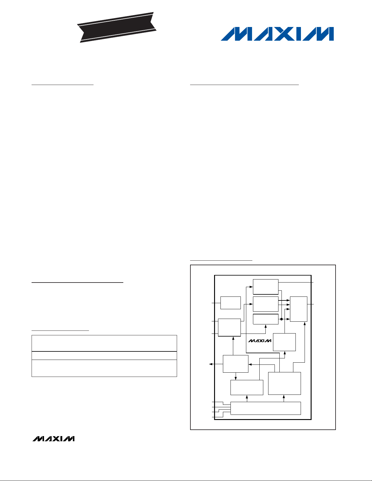
General Description
The MAX6955 is a compact display driver that interfaces
microprocessors to a mix of 7-segment, 14-segment,
and 16-segment LED displays through an I2C-compatible 2-wire serial interface. The MAX6955 drives up to 16
digits 7-segment, 8 digits 14-segment, 8 digits 16-segment, or 128 discrete LEDs, while functioning from a
supply voltage as low as 2.7V. The driver includes five
I/O expander or general-purpose I/O (GPIO) lines, some
or all of which can be configured as a key-switch reader.
The key-switch reader automatically scans and
debounces a matrix of up to 32 switches.
Included on chip are full 14- and 16-segment ASCII
104-character fonts, a hexadecimal font for 7-segment
displays, multiplex scan circuitry, anode and cathode
drivers, and static RAM that stores each digit. The maximum segment current for the display digits is set using
a single external resistor. Digit intensity can be independently adjusted using the 16-step internal digital
brightness control. The MAX6955 includes a low-power
shutdown mode, a scan-limit register that allows the
user to display from 1 to 16 digits, segment blinking
(synchronized across multiple drivers, if desired), and a
test mode, which forces all LEDs on. The LED drivers
are slew-rate limited to reduce EMI.
For an SPI™-compatible version, refer to the MAX6954
data sheet. An evaluation kit (EV kit) for the MAX6955 is
available.
Applications
Set-Top Boxes Automotive
Panel Meters Bar Graph Displays
White Goods Audio/Video Equipment
Features
♦ 400kbps 2-Wire I2C-Compatible Interface
♦ 2.7V to 5.5V Operation
♦ Drives Up to 16 Digits 7-Segment, 8 Digits
14-Segment, 8 Digits 16-Segment, 128 Discrete
LEDs, or a Combination of Digit Types
♦ Drives Common-Cathode Monocolor and Bicolor
LED Displays
♦ Built-In ASCII 104-Character Font for 14-Segment
and 16-Segment Digits and Hexadecimal Font for
7-Segment Digits
♦ Automatic Blinking Control for Each Segment
♦ 10µA (typ) Low-Power Shutdown (Data Retained)
♦ 16-Step Digit-by-Digit Digital Brightness Control
♦ Display Blanked on Power-Up
♦ Slew-Rate-Limited Segment Drivers for Lower EMI
♦ Five GPIO Port Pins Can Be Configured as Key-
Switch Reader to Scan and Debounce Up to 32
Switches with n-Key Rollover
♦ IRQ Output when a Key Input is Debounced
♦ 36-Pin SSOP and 40-Pin TQFN Packages
♦ Automotive Temperature Range Standard
MAX6955
2-Wire Interfaced, 2.7V to 5.5V LED Display
Driver with I/O Expander and Key Scan
________________________________________________________________ Maxim Integrated Products 1
Ordering Information
19-2548; Rev 2; 12/06
For pricing, delivery, and ordering information, please contact Maxim/Dallas Direct! at
1-888-629-4642, or visit Maxim’s website at www.maxim-ic.com.
PART
TEMP RANGE
PINPACKAGE
PKG
CODE
MAX6955AAX
36 SSOP A36-2
MAX6955ATL+
T4066- 5
Pin Configurations and Typical Operating Circuits appear
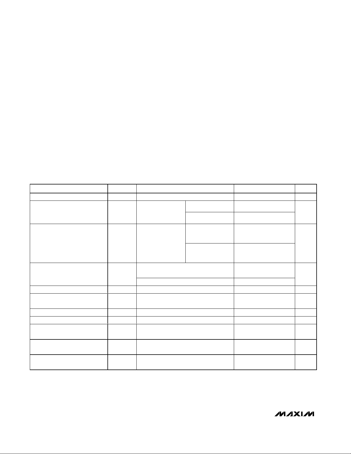
at end of data sheet.
ISET
OSC
OSC_OUT
BLINK
SCL
AD0
AD1
SDA
2-WIRE SERIAL INTERFACE
RAM
BLINK
CONTROL
CONFIGURATION
REGISTER
CHARACTER
GENERATOR
ROM
CURRENT
SOURCE
DIVIDER/
COUNTER
NETWORK
DIGIT
MULTIPLEXER
PWM
BRIGHTNESS
CONTROL
GPIO
AND KEY-SCAN
CONTROL
LED
DRIVERS
O0 TO O18
P0 TO P4
MAX6955
Functional Diagram
EVALUATION KIT
AVAILABLE
SPI is a trademark of Motorola, Inc.
*EP = Exposed paddle.
+Denotes lead-free package.
-40°C to +125°C
-40°C to +125°C
40 TQFN-EP*
(6mm x 6mm)
Page 2
MAX6955
2-Wire Interfaced, 2.7V to 5.5V LED Display
Driver with I/O Expander and Key Scan
2 _______________________________________________________________________________________
ABSOLUTE MAXIMUM RATINGS
Stresses beyond those listed under “Absolute Maximum Ratings” may cause permanent damage to the device. These are stress ratings only, and functional
operation of the device at these or any other conditions beyond those indicated in the operational sections of the specifications is not implied. Exposure to
absolute maximum rating conditions for extended periods may affect device reliability.
Voltage (with Respect to GND)
V+ .........................................................................-0.3V to +6V
SCL, SDA, AD0, AD1 ...........................................-0.3V to +6V
All Other Pins............................................-0.3V to (V+ + 0.3V)
Current
O0–O7 Sink Current ......................................................935mA
O0–O18 Source Current .................................................55mA
SCL, SDA, AD0, AD1, BLINK, OSC, OSC_OUT, ISET ....20mA
P0, P1, P2, P3, P4 ...........................................................40mA
GND .....................................................................................1A
Continuous Power Dissipation (T
A
= +70°C)
36-Pin SSOP (derate at 11.8mW/°C above +70°C) .....941mW
40-Pin TQFN (derate at 25.6mW/°C above +70°C)....2051.3mW
Operating Temperature Range
(T
MIN
to T
MAX
) ...............................................-40°C to +125°C
Junction Temperature......................................................+150°C
Storage Temperature Range .............................-65°C to +150°C
Lead Temperature (soldering, 10s) .................................+300°C
DC ELECTRICAL CHARACTERISTICS
(Typical Operating Circuit, V+ = 2.7V to 5.5V, TA= T
MIN
to T
MAX
, unless otherwise noted.) (Note 1)
PARAMETER
CONDITIONS
UNITS
Operating Supply Voltage V+ 2.7 5.5 V
TA = +25°C 10 35
Shutdown Supply Current I
SHDN
Shutdown mode, all
digital inputs at V+
or GND
T
A
= T
MIN
to T
MAX
40
µA
TA = +25°C 22 30
Operating Supply Current I+
All segments on, all
digits scanned,
intensity set to full,
internal oscillator, no
display or OSC_OUT
load connected
T
A
= T
MIN
to T
MAX
35
mA
OSC = RC oscillator, R
SET
= 56kΩ,
C
SET
= 22pF, V+ = 3.3V
4
Master Clock Frequency f
OSC
OSC driven externally 1 8
MHz
Dead Clock Protection Frequency
f
OSC
95 kHz
OSC Internal/External Detection
Threshold
V
OSC
1.7 V
OSC High Time t
CH
50 ns
OSC Low Time t
CL
50 ns
Slow Segment Blink Period
OSC = RC oscillator, R
SET
= 56kΩ,
C
SET
= 22pF, V+ = 3.3V
1s
Fast Segment Blink Period
OSC = RC oscillator, R
SET
= 56kΩ,
C
SET
= 22pF, V+ = 3.3V
0.5 s
Fast or Slow Segment Blink Duty
Cycle
%
SYMBOL
MIN TYP MAX
f
SLOWBLINK
f
FASTBLINK
49.5 50.5
Page 3
MAX6955
2-Wire Interfaced, 2.7V to 5.5V LED Display
Driver with I/O Expander and Key Scan
_______________________________________________________________________________________ 3
DC ELECTRICAL CHARACTERISTICS (continued)
(Typical Operating Circuit, V+ = 2.7V to 5.5V, TA= T
MIN
to T
MAX
, unless otherwise noted.) (Note 1)
PARAMETER
CONDITIONS
UNITS
V
LED
= 2.2V,
V+
= 3.3V
Segment Drive Source Current I
SEG
V
LED
= 2.2V,
V+
= 2.7V
T
A
= +25°C -32 -40 -48 mA
Segment Current Slew Rate
TA = +25°C, V+ = 3.3V 11
mA/µs
Segment Drive Current Matching
∆I
SEG
TA = +25°C, V+ = 3.3V 5 %
LOGIC INPUTS AND OUTPUTS
Input High Voltage
SDA, SCL, AD0, AD1
V
IH
0.7 x
V+
V
Input Low Voltage
SDA, SCL, AD0, AD1
V
IL
0.3 x
V+
V
Input Leakage Current
SDA, SCL, AD0, AD1, OSC, P0,
P1, P2, P3, P4
I
IH
, I
IL
-1 +1 µA
SDA Output Low Voltage V
OLSDAISINK
= 6mA 0.4 V
Port Logic-High Input Voltage
P0, P1, P2, P3, P4
V
IHP
0.7 x
V+
V
Port Logic-Low Input Voltage
P0, P1, P2, P3, P4
V
ILP
0.3 x
V+
V
Port Hysteresis Voltage
P0, P1, P2, P3, P4
∆V
IP
0.03 x
V+
V
Port Input Pullup Current from V+
I
IPU
P0 to P3 configured as key-scan inputs,
V+ = 3.3V
75 µA
Port Output Low Voltage V
OLP
I
SINK
= 8mA 0.3 0.5 V
Blink Output Low Voltage V
OLBKISINK
= 0.6mA 0.1 0.3 V
OSC_OUT Output High Voltage
I
SOURCE
= 1.6mA
V+ -
0.4
V
OSC_OUT Output Low Voltage
I
SINK
= 1.6mA 0.4 V
SYMBOL
∆I
SEG
/∆t
MIN TYP MAX
V
OHOSC
V
OLOSC
Page 4
MAX6955
2-Wire Interfaced, 2.7V to 5.5V LED Display
Driver with I/O Expander and Key Scan
4 _______________________________________________________________________________________
TIMING CHARACTERISTICS
(Typical Operating Circuit, V+ = 2.7V to 5.5V, TA= T
MIN
to T
MAX
, unless otherwise noted.) (Note 1)
PARAMETER
CONDITIONS
UNITS
TIMING CHARACTERISTICS
Serial Clock Frequency f
SCL
kHz
Bus Free Time Between a STOP
and a START Condition
t
BUF
1.3 µs
Hold Time (Repeated) START
Condition
,
0.6 µs
Repeated START Condition Setup
Time
0.6 µs
STOP Condition Setup Time
0.6 µs
Data Hold Time
(Note 3) 0.9 µs
Data Setup Time
ns
SCL Clock Low Period t
LOW
1.3 µs
SCL Clock High Period t
HIGH
0.6 µs
Rise Time of Both SDA and SCL
Signals, Receiving
t
R
(Notes 2, 4)
20 +
ns
Fall Time of Both SDA and SCL
Signals, Receiving
t
F
(Notes 2, 4)
20 +
ns
Fall Time of SDA Transmitting tF, t
X
(Notes 2, 5)
20 +
ns
Pulse Width of Spike Suppressed t
SP
(Notes 2, 6) 0 50 ns
Capacitive Load for Each
Bus Line
C
B
(Note 2)
pF
Note 1: All parameters tested at TA= +25°C. Specifications over temperature are guaranteed by design.
Note 2: Guaranteed by design.
Note 3: A master device must provide a hold time of at least 300ns for the SDA signal (referred to V
IL
- of the SCL signal) in order to
bridge the undefined region of SCL’s falling edge.
Note 4: C
B
= total capacitance of one bus line in pF. tRand tFmeasured between 0.3V+ and 0.7V+.
Note 5: I
SINK
≤ 6mA. CB= total capacitance of one bus line in pF. tRand tFmeasured between 0.3V+ and 0.7V+.
Note 6: Input filters on the SDA and SCL inputs suppress noise spikes less than 50ns.
SYMBOL
MIN TYP MAX
400
t
t
HD
STA
tSU, t
STA
t
SU:STO
tHD, t
DAT
tSU, t
DAT
100
B
B
B
300
300
300
0.1C
0.1C
0.1C
400
Page 5
MAX6955
2-Wire Interfaced, 2.7V to 5.5V LED Display
Driver with I/O Expander and Key Scan
_______________________________________________________________________________________ 5
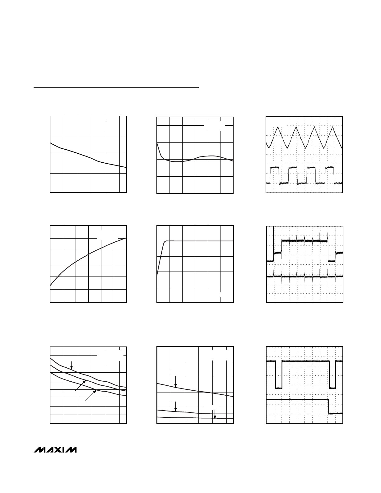
Typical Operating Characteristics
(V+ = 3.3V, LED forward voltage = 2.4V, Typical Application Circuit, TA= +25°C, unless otherwise noted.)
INTERNAL OSCILLATOR FREQUENCY
vs. TEMPERATURE
MAX6955 toc01
TEMPERATURE (°C)
OSCILLATOR FREQUENCY (MHz)
110805020-10
3.8
4.0
4.2
4.4
3.6
-40
R
SET
= 56kΩ
C
SET
= 22pF
SUPPLY VOLTAGE (V)
5.04.54.03.53.02.5 5.5
INTERNAL OSCILLATOR FREQUENCY
vs. SUPPLY VOLTAGE
MAX6955 toc02
OSCILLATOR FREQUENCY (MHz)
3.8
4.0
4.2
4.4
3.6
R
SET
= 56kΩ
C
SET
= 22pF
100ns/div
OSC: 500mV/div
OSC_OUT: 2V/div
MAX6954 toc03
OSC
0V
0V
OSC_OUT
INTERNAL OSCILLATOR WAVEFORM
AT OSC AND OSC_OUT PINS
R
SET
= 56kΩ
C
SET
= 22pF
DEAD CLOCK OSCILLATOR FREQUENCY
vs. SUPPLY VOLTAGE
85
90
95
100
105
110
80
SUPPLY VOLTAGE (V)
5.04.54.03.53.02.5 5.5
MAX6955 toc04
OSCILLATOR FREQUENCY (MHz)
R
SET
= 56kΩ
C
SET
= GND
CURRENT NORMALIZED TO 40mA
0.94
0.96
0.98
1.00
1.02
0.92
SEGMENT SOURCE CURRENT
vs. SUPPLY VOLTAGE
SUPPLY VOLTAGE (V)
5.04.54.03.53.02.5 5.5
MAX6955 toc05
V
LED
= 1.8V
1V/div
200µs/div
MAX6954 toc06
O0
O18
WAVEFORM AT PINS O0 AND O18,
MAXIMUM INTENSITY
0V
0V
GPIO SINK CURRENT
vs. TEMPERATURE
MAX 6955 toc07
TEMPERATURE (°C)
GPIO SINK CURRENT (mA)
110805020-10
5
10
15
20
25
30
35
40
45
0
-40
VCC = 5.5V
VCC = 3.3V
VCC = 2.5V
OUTPUT = LOW
V
PORT
= 0.6V
PORT INPUT PULLUP CURRENT
vs. TEMPERATURE
MAX6955 toc08
TEMPERATURE (°C)
KEY-SCAN SOURCE CURRENT (mA)
110805020-10
0.1
0.2
0.3
0.4
0.5
0
-40
VCC = 5.5V
VCC = 3.3V
VCC = 2.5V
OUTPUT = HIGH
V
PORT
= 1.4V
400µs/div
KEY_A: 1V/div
IRQ: 2V/div
MAX6954 toc09
KEY_A
0V
0V
IRQ
KEY-SCAN OPERATION
(KEY_A AND IRQ)
Page 6
MAX6955
Detailed Description
The MAX6955 is a serially interfaced display driver that
can drive up to 16 digits 7-segment, 8 digits 14-segment, 8 digits 16-segment, 128 discrete LEDs, or a
combination of these display types. Table 1 shows the
drive capability of the MAX6955 for monocolor and
bicolor displays.
The MAX6955 includes 104-character ASCII font maps
for 14-segment and 16-segment displays, as well as
the hexadecimal font map for 7-segment displays. The
characters follow the standard ASCII font, with the addition of the following common symbols: £, A€ , ¥, °, µ, ±,
↑, and ↓. Seven bits represent the 104-character font
map; an 8th bit is used to select whether the decimal
point (DP) is lit. Seven-segment LED digits can be controlled directly or use the hexadecimal font. Direct segment control allows the MAX6955 to be used to drive
bar graphs and discrete LED indicators.
Tables 2, 3, and 4 list the connection schemes for 16-,
14-, and 7-segment digits, respectively. The letters in
Tables 2, 3, and 4 correspond to the segment labels
shown in Figure 1. (For applications that require mixed
display types, see Tables 38–41.)
Serial Interface
Serial Addressing
The MAX6955 operates as a slave that sends and
receives data through an I2C-compatible 2-wire interface. The interface uses a serial data line (SDA) and a
2-Wire Interfaced, 2.7V to 5.5V LED Display
Driver with I/O Expander and Key Scan
6 _______________________________________________________________________________________
Pin Description
PIN
SSOP
NAME FUNCTION
1, 2,
34, 35, 36
36, 37,
P0–P4
General-Purpose I/O Ports (GPIOs). GPIO can be configured as logic inputs or open-drain
outputs. Enabling key scanning configures some or all ports P0–P3 as key-switch matrix inputs
with internal pullup and port P4 as IRQ output.
3 38 AD0
Address Input 0. Sets device slave address. Connect to GND, V+, SCL, or SDA to give four
logic combinations. See Table 5.
4 39 SDA I2C-Compatible Serial Data I/O
5 40 SCL I2C-Compatible Serial Clock Input
6 1 AD1
Address Input 1. Sets device slave address. Connect to GND, V+, SCL, or SDA to give four
logic combinations. See Table 5.
7–15,
22–31
2–10,
21–30
Digit/Segment Drivers. When acting as digit drivers, outputs O0 to O7 sink current from the
display common cathodes. When acting as segment drivers, O0 to O18 source current to the
display anodes. O0 to O18 are high impedance when not being used as digit or segment
drivers.
16, 18
GND Ground
17 14 ISET
Segment Current Setting. Connect ISET to GND through series resistor R
SET
to set the peak
current.
19, 21
V+
Positive Supply Voltage. Bypass V+ to GND with a 47µF bulk capacitor and a 0.1µF ceramic
capacitor.
20 17 OSC
Multiplex Clock Input. To use internal oscillator, connect capacitor C
SET
from OSC to GND.
To use external clock, drive OSC with a 1MHz to 8MHz CMOS clock.
32 31 BLINK Blink Clock Output. Output is open drain.
33 32
Clock Output. OSC_OUT is a buffered clock output to allow easy blink synchronization of
multiple MAX6955s. Output is push-pull.
—
N.C. Not Internally Connected
—EP EP
Exposed Paddle. Internally connected to GND. Connect to a large ground plane to improve
thermal performance.
TQFN
33, 34, 35
O0–O18
12, 13, 15
16, 18, 19
11, 20
OSC_OUT
Page 7
MAX6955
2-Wire Interfaced, 2.7V to 5.5V LED Display
Driver with I/O Expander and Key Scan
_______________________________________________________________________________________ 7
serial clock line (SCL) to achieve bidirectional communication between master(s) and slave(s). A master (typically a microcontroller) initiates all data transfers to and
from the MAX6955, and generates the SCL clock that
synchronizes the data transfer (Figure 2).
The MAX6955 SDA line operates as both an input and
an open-drain output. A pullup resistor, typically 4.7kΩ,
is required on the SDA. The MAX6955 SCL line operates only as an input. A pullup resistor, typically 4.7kΩ,
is required on SCL if there are multiple masters on the
2-wire interface, or if the master in a single-master system has an open-drain SCL output.
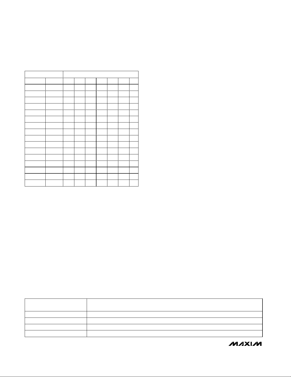
Each transmission consists of a START condition
(Figure 3) sent by a master, followed by the MAX6955
7-bit slave address plus R/W bit (Figure 4), a register
address byte, 1 or more data bytes, and finally a STOP
condition (Figure 3).
Start and Stop Conditions
Both SCL and SDA remain high when the interface is
not busy. A master signals the beginning of a transmission with a START (S) condition by transitioning SDA
from high to low while SCL is high. When the master
has finished communicating with the slave, it issues a
STOP (P) condition by transitioning the SDA from low to
high while SCL is high. The bus is then free for another
transmission (Figure 3).
Bit Transfer
One data bit is transferred during each clock pulse.
The data on the SDA line must remain stable while SCL
is high (Figure 5).
Acknowledge
The acknowledge bit is a clocked 9th bit that the recipient
uses to handshake receipt of each byte of data (Figure 6).
Thus, each byte transferred effectively requires 9 bits. The
master generates the 9th clock pulse, and the recipient
pulls down SDA during the acknowledge clock pulse, such
that the SDA line is stable low during the high period of the
clock pulse. When the master is transmitting to the
MAX6955, the MAX6955 generates the acknowledge bit
because the MAX6955 is the recipient. When the MAX6955
is transmitting to the master, the master generates the
acknowledge bit because the master is the recipient.
Slave Address
The MAX6955 has a 7-bit-long slave address (Figure
4). The eighth bit following the 7-bit slave address is the
R/W bit. It is low for a write command, high for a read
command.
The first 3 bits (MSBs) of the MAX6955 slave address
are always 110. Slave address bits A3, A2, A1, and A0
are selected by the address input pins AD1 and AD0.
These two input pins can be connected to GND, V+,
SDA, or SCL. The MAX6955 has 16 possible slave
addresses (Table 5) and therefore a maximum of 16
MAX6955 devices can share the same interface.
DISPLAY TYPE
7 SEGMENT
(16-CHARACTER
HEXADECIMAL FONT)
14 SEGMENT/
16 SEGMENT
(104-CHARACTER ASCII FONT MAP)
DISCRETE LEDs
(DIRECT CONTROL)
Monocolor 16 8 128
Bicolor 8 4 64
Table 1. MAX6955 Drive Capability
1dp
2dp
fb
ec
d2
a1
i
l
g1 g2
hj
mk
a2
d1
dp dp
1a
1g
1f
1b
1e 1c
1d
2a
2g
2f 2b
2e 2c
2d
fb
ec
d
a
i
l
g1 g2
hj
mk
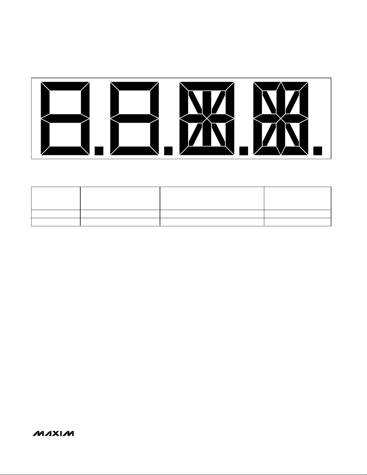
Figure 1. Segment Labeling for 7-Segment Display, 14-Segment Display, and 16-Segment Display
Page 8
MAX6955
2-Wire Interfaced, 2.7V to 5.5V LED Display
Driver with I/O Expander and Key Scan
8 _______________________________________________________________________________________
Message Format for Writing
A write to the MAX6955 comprises the transmission of
the MAX6955’s slave address with the R/W bit set to
zero, followed by at least 1 byte of information. The first
byte of information is the command byte, which determines which register of the MAX6955 is to be written by
the next byte, if received. If a STOP condition is detected after the command byte is received, then the
MAX6955 takes no further action (Figure 7) beyond
storing the command byte.
Any bytes received after the command byte are data
bytes. The first data byte goes into the internal register of
the MAX6955 selected by the command byte (Figure 8).
If multiple data bytes are transmitted before a STOP
condition is detected, these bytes are generally stored
in subsequent MAX6955 internal registers because the
command byte address generally autoincrements
(Table 6) (Figure 9).
DIGIT
O18
0
f
ij
l
dp
1
f
ij
l
dp
2
f
ij
l
dp
3
f
ij
l
dp
4
f
ij
l
dp
5
f
ij
l
dp
6
f
ij
l
dp
7
f
ij
l
dp
Table 2. Connection Scheme for Eight 16-Segment Digits
Table 3. Connection Scheme for Eight 14-Segment Digits
DIGIT
O18
0, 0a
2dp
1, 1a
2dp
2, 2a
2dp
3, 3a
2dp
4, 4a
2dp
5, 5a
2dp
6, 6a
2dp
7, 7a
2dp
Table 4. Connection Scheme for Sixteen 7-Segment Digits
O0 O1 O2 O3 O4 O5 O6 O7 O8 O9 O10 O11 O12 O13 O14 O15 O16 O17
CCO — a1 a2 b c d1 d2 e
— CC1 a1 a2 b c d1 d2 e
a1 a2 CC2 — b c d1 d2 e
a1 a2 — CC3 b c d1 d2 e
a1 a2 b c CC4 — d1 d2 e
a1 a2 b c — CC5 d1 d2 e
a1 a2 b c d1 d2 CC6 — e
a1 a2 b c d1 d2 — CC7 e
DIGIT O0 O1 O2 O3 O4 O5 O6 O7 O8 O9 O10 O11 O12 O13 O14 O15 O16 O17 O18
0 CCO — a — b c d — e f g1 g2 h i j k l m dp
1 — CC1 a — b c d — e f g1 g2 h i j k l m dp
2 a — CC2 — b c d — e f g1 g2 h i j k l m dp
3 a — — CC3 b c d — e f g1 g2 h i j k l m dp
4 a—b cCC4—d—e fg1g2h i j k l mdp
5 a — b c — CC5 d — e f g1 g2 h i j k l m dp
6 a—b c d—CC6—e fg1g2h i j k l mdp
7 a — b c d — — CC7 e f g1 g2 h i j k l m dp
g1 g2 h
g1 g2 h
g1 g2 h
g1 g2 h
g1 g2 h
g1 g2 h
g1 g2 h
g1 g2 h
k
k
k
k
k
k
k
k
m
m
m
m
m
m
m
m
O0 O1 O2 O3 O4 O5 O6 O7 O8 O9 O10 O11 O12 O13 O14 O15 O16 O17
CC0 — 1a — 1b 1c 1d 1dp 1e 1f 1g 2a 2b 2c 2d 2e 2f 2g
— CC1 1a — 1b 1c 1d 1dp 1e 1f 1g 2a 2b 2c 2d 2e 2f 2g
1a — CC2 — 1b 1c 1d 1dp 1e 1f 1g 2a 2b 2c 2d 2e 2f 2g
1a — — CC3 1b 1c 1d 1dp 1e 1f 1g 2a 2b 2c 2d 2e 2f 2g
1a — 1b 1c CC4 — 1d 1dp 1e 1f 1g 2a 2b 2c 2d 2e 2f 2g
1a — 1b 1c — CC5 1d 1dp 1e 1f 1g 2a 2b 2c 2d 2e 2f 2g
1a—1b1c1d1dpCC6— 1e 1f 1g2a2b2c2d2e2f 2g
1a — 1b 1c 1d 1dp — CC7 1e 1f 1g 2a 2b 2c 2d 2e 2f 2g
Page 9
MAX6955
2-Wire Interfaced, 2.7V to 5.5V LED Display
Driver with I/O Expander and Key Scan
_______________________________________________________________________________________ 9
SDA
START CONDITION STOP CONDITION
SCL
S
P
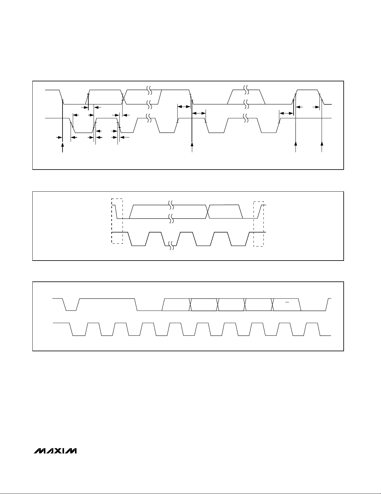
Figure 3. Start and Stop Conditions
Figure 4. Slave Address
SDA
t
LOW
t
BUF
t
SU, DAT
t
SU, STA
t
HD, STA
t
SU, STO
t
HD, DAT
t
HIGH
t
R
t
F
SCL
START
CONDITION
START
CONDITION
STOP
CONDITION
REPEATED START
CONDITION
t
HD, STA
Figure 2. 2-Wire Serial Interface Timing Details
SDA
SCL
1
MSBSTART
1
0
A3
A2
A1 A0
LSB
R/W
ACK
Page 10
MAX6955
2-Wire Interfaced, 2.7V to 5.5V LED Display
Driver with I/O Expander and Key Scan
10 ______________________________________________________________________________________
Message Format for Reading
The MAX6955 is read using the MAX6955’s internally
stored command byte as address pointer, the same
way the stored command byte is used as address
pointer for a write. The pointer generally autoincrements after each data byte is read using the same rules
as for a write (Table 6). Thus, a read is initiated by first
configuring the MAX6955’s command byte by performing a write (Figure 7). The master can now read n consecutive bytes from the MAX6955, with the first data
byte being read from the register addressed by the initialized command byte (Figure 9). When performing
read-after-write verification, reset the command byte’s
address because the stored byte address generally is
autoincremented after the write (Table 6).
Operation with Multiple Masters
If the MAX6955 is operated on a 2-wire interface with
multiple masters, a master reading the MAX6955
should use a repeated start between the write, which
sets the MAX6955’s address pointer, and the read(s)
that takes the data from the location(s). This is because
it is possible for master 2 to take over the bus after
master 1 has set up the MAX6955’s address pointer but
before master 1 has read the data. If master 2 subsequently changes the MAX6955’s address pointer, then
master 1’s delayed read may be from an unexpected
location.
Command Address Autoincrementing
Address autoincrementing allows the MAX6955 to be
configured with the shortest number of transmissions by
minimizing the number of times the command byte
needs to be sent. The command address or the font
pointer address stored in the MAX6955 generally increments after each data byte is written or read (Table 6).
To utilize the autoincrement read cycle feature, the master clocks SCL after the first data byte is read, and the
MAX6955 continues sending data, incrementing the
pointer after each byte is sent. A not-acknowledge or
stop condition halts autoincrement.
Digit Type Registers
The MAX6955 uses 32 digit registers to store the characters that the user wishes to display. These digit registers are implemented with two planes, P0 and P1. Each
digit is represented by 2 bytes of memory, 1 byte in
plane P0 and the other in plane P1. The digit registers
are mapped so that a digit’s data can be updated in
plane P0, plane P1, or both planes at the same time
(Table 7).
If the blink function is disabled through the Blink Enable
Bit E (Table 20) in the configuration register, then the
digit register data in plane P0 is used to multiplex the
display. The digit register data in P1 is not used. If the
blink function is enabled, then the digit register data in
both plane P0 and plane P1 are alternately used to multiplex the display. Blinking is achieved by multiplexing
the LED display using data plane P0 and plane P1 on
alternate phases of the blink clock (Table 21).
COMMAND BYTE
ADDRESS RANGE
AUTOINCREMENT BEHAVIOR
x0000000 to x0001100 Command byte address autoincrements after byte read or written.
x0001101 Factory reserved; do not write this register.
x0001111 to x1111110 Command byte address autoincrements after byte read or written.
x1111111 Command byte address remains at x1111111 after byte read or written.
Table 5. MAX6955 Address Map
Table 6. Command Address Autoincrement Rules
PIN CONNECTION
DEVICE ADDRESS
AD1
A0
GND
0
GND V+
1
GND
0
GND
1
V+
0
V+ V+
1
V+
0
V+
1
SDA
0
SDA V+
1
SDA
0
SDA
1
SCL
0
SCL V+
1
SCL
0
SCL
1
AD0 A6A5A4A3A2A1
GND110000
110000
SDA110001
SCL 110001
GND110010
110010
SDA110011
SCL 110011
GND110100
110100
SDA110101
SCL 110101
GND110110
110110
SDA110111
SCL 110111
Page 11

MAX6955
2-Wire Interfaced, 2.7V to 5.5V LED Display
Driver with I/O Expander and Key Scan
______________________________________________________________________________________ 11
The data in the digit registers does not control the digit
segments directly for 14- and 16-segment displays.
Instead, the register data is used to address a character generator that stores the data for the 14- and 16segment fonts (Tables 8 and 9). The lower 7 bits of the
digit data (D6 to D0) select the character from the font.
The most significant bit of the register data (D7) controls the DP segment of the digits; it is set to 1 to light
DP, and to zero to leave DP unlit (Table 10).
For 7-segment displays, the digit plane data register
can be used to address a character generator, which
contains the data of a 16-character font containing the
hexadecimal font. The decode mode register can be
used to disable the character generator and allow the
segments to be controlled directly. Table 11 shows the
one-to-one pairing of each data bit to the appropriate
segment line in the digit plane data registers. The hexadecimal font is decoded according to Table 12.
The digit-type register configures the display driver for
various combinations of 14-segment digits, 16-segment
digits, and/or pairs, or 7-segment digits. The function of
this register is to select the appropriate font for each
digit and route the output of the font to the appropriate
MAX6955 driver output pins. The MAX6955 has four
digit drive slots. A slot can be filled with various combinations of monocolor and bicolor 16-segment displays,
14-segment displays, or two 7-segment displays. Each
pair of bits in the register corresponds to one of the four
digit drive slots, as shown in Table 13. Each bit also corresponds to one of the eight common-cathode digit
drive outputs, CC0 to CC7. When using bicolor digits,
the anode connections for the two digits within a slot are
always the same. This means that a slot correctly drives
two monocolor or one bicolor 14- or 16-segment digit.
The digit type register can be written, but cannot be
read. Examples of configuration settings required for
some display digit combinations are shown in Table 14.
7-Segment Decode-Mode Register
In 7-segment mode, the hexadecimal font can be disabled (Table 15). The decode-mode register selects
between hexadecimal code or direct control for each of
eight possible pairs of 7-segment digits. Each bit in the
register corresponds to one pair of digits. The digit
pairs are {digit 0, digit 0a} through {digit 7, digit 7a}.
Disabling decode mode allows direct control of the 16
LEDs of a dual 7-segment display. Direct control mode
can also be used to drive a matrix of 128 discrete LEDs.
A logic high selects hexadecimal decoding, while a
logic low bypasses the decoder. When direct control is
selected, the data bits D7 to D0 correspond to the segment lines of the MAX6955. Write x0010000 to blank all
segments in hexadecimal decode mode.
Display Blink Mode
The display blinking facility, when enabled, makes the
driver flip automatically between displaying the digit
register data in planes P0 and P1. If the digit register
data for any digit is different in the two planes, then that
digit appears to flip between two characters. To make a
character appear to blink on or off, write the character
to one plane, and use the blank character (0x20) for the
other plane. Once blinking has been configured, it continues automatically without further intervention.
Blink Speed
The blink speed is determined by the frequency of the
multiplex clock, OSC, and by the setting of the Blink
Rate Selection Bit B (Table 19) in the configuration register. The Blink Rate Selection Bit B sets either fast or
slow blink speed for the whole display.
Initial Power-Up
On initial power-up, all control registers are reset, the
display is blanked, intensities are set to minimum, and
shutdown is enabled (Table 16).
Configuration Register
The configuration register is used to enter and exit shutdown, select the blink rate, globally enable and disable
the blink function, globally clear the digit data, select
between global or digit-by-digit control of intensity, and
reset the blink timing (Tables 17–20 and 22–25).
The configuration register contains 7 bits:
• S bit selects shutdown or normal operation
(read/write).
• B bit selects the blink rate (read/write).
• E bit globally enables or disables the blink function
(read/write).
• T bit resets the blink timing (data is not stored—transient bit).
• R bit globally clears the digit data for both planes P0
and P1 for ALL digits (data is not stored—transient bit).
• I bit selects between global or digit-by-digit control
of intensity (read/write).
• P bit returns the current phase of the blink timing
(read only—a write to this bit is ignored).
Character Generator Font Mapping
The font is composed of 104 characters in ROM. The
lower 7 bits of the 8-bit digit register represent the character selection. The most significant bit, shown as x in
the ROM map of Tables 8 and 9, is 1 to light the DP
segment and zero to leave the DP segment unlit.
The character map follows the standard ASCII font for
96 characters in the x0101000 through x1111111
Page 12

MAX6955
2-Wire Interfaced, 2.7V to 5.5V LED Display
Driver with I/O Expander and Key Scan
12 ______________________________________________________________________________________
range. The first 16 characters of the 16-segment ROM
map cover 7-segment displays. These 16 characters
are numeric 0 to 9 and characters A to F (i.e., the hexadecimal set).
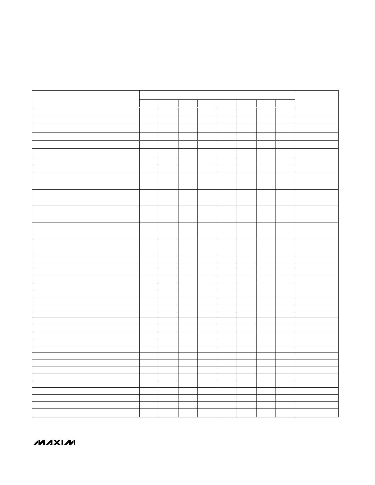
Multiplex Clock and Blink Timing
The OSC pin can be fitted with capacitor C
SET
to GND to
use the internal RC multiplex oscillator, or driven by an
external clock to set the multiplex clock frequency and
blink rate. The multiplex clock frequency determines the
frequency that the complete display is updated. With
OSC at 4MHz, each display digit is enabled for 200µs.
The internal RC oscillator uses an external resistor,
R
SET
, and an external capacitor, C
SET
, to set the oscil-
lator frequency. The suggested values of R
SET
(56kΩ)
and C
SET
(22pF) set the oscillator at 4MHz, which
makes the blink frequency 0.5Hz or 1Hz.
The external clock is not required to have a 50:50 duty
cycle, but the minimum time between transitions must
be 50ns or greater and the maximum time between
transitions must be 750ns.
The on-chip oscillator may be accurate enough for
applications using a single device. If an exact blink rate
is required, use an external clock ranging between
1MHz and 8MHz to drive OSC. The OSC inputs of multiple MAX6955s can be connected to a common external
clock to make the devices blink at the same rate. The
relative blink phasing of multiple MAX6955s can be synchronized by setting the T bit in the control register for
all the devices in quick succession. If the serial interfaces of multiple MAX6955s are daisy-chained by connecting the DOUT of one device to the DIN of the next,
then synchronization is achieved automatically by
updating the configuration register for all devices simultaneously. Figure 10 is the multiplex timing diagram.
OSC_OUT Output
The OSC_OUT output is a buffered copy of either the
internal oscillator clock or the clock driven into the OSC
pin if the external clock has been selected. The feature
is useful if the internal oscillator is used, and the user
wishes to synchronize other MAX6955s to the same
blink frequency. The oscillator is disabled while the
MAX6955 is in shutdown.
Scan-Limit Register
The scan-limit register sets how many 14-segment digits or 16-segment digits or pairs of 7-segment digits are
displayed, from 1 to 8. A bicolor digit is connected as
two monocolor digits. The scan register also limits the
number of keys that can be scanned.
Since the number of scanned digits affects the display
brightness, the scan-limit register should not be used to
blank portions of the display (such as leading-zero suppression). Table 26 shows the scan-limit register format.
Intensity Registers
Digital control of display brightness is provided and
can be managed in one of two ways: globally or individually. Global control adjusts all digits together.
Individual control adjusts the digits separately.
The default method is global brightness control, which
is selected by clearing the global intensity bit (I data bit
D6) in the configuration register. This brightness setting
applies to all display digits. The pulse-width modulator
is then set by the lower nibble of the global intensity
register, address 0x02. The modulator scales the average segment current in 16 steps from a maximum of
15/16 down to 1/16 of the peak current. The minimum
interdigit blanking time is set to 1/16 of a cycle. When
using bicolor digits, 256 color/brightness combinations
are available.
Individual brightness control is selected by setting the
global intensity bit (I data bit D6) in the configuration
register. The pulse-width modulator is now no longer
set by the lower nibble of the global intensity register,
address 0x02, and the data is ignored. Individual digital control of display brightness is now provided by a
separate pulse-width modulator setting for each digit.
Each digit is controlled by a nibble of one of the four
intensity registers: intensity10, intensity32, intensity54,
and intensity76 for all display types, plus intensity10a,
intensity32a, intensity54a, and intensity76a for the extra
eight digits possible when 7-segment displays are
used. The data from the relevant register is used for
each digit as it is multiplexed. The modulator scales the
average segment current in 16 steps in exactly the
same way as global intensity adjustment.
Table 27 shows the global intensity register format. Table
28 shows individual segment intensity registers. Table 29
shows the even individual segment intensity format. Table
30 shows the odd individual segment intensity format.
GPIO and Key Scanning
The MAX6955 features five general-purpose input/output (GPIO) ports: P0 to P4. These ports can be individually enabled as logic inputs or open-drain logic
outputs. The GPIO ports are not debounced when configured as inputs. The ports can be read and the outputs set using the 2-wire interface.
Some or all of the five ports can be configured to perform key scanning of up to 32 keys. Ports P0 to P4 are
renamed Key_A, Key_B, Key_C, Key_D, and IRQ,
respectively, when used for key scanning. The full keyscanning configuration is shown in Figure 11. Table 31
is the GPIO data register.
Page 13
MAX6955
2-Wire Interfaced, 2.7V to 5.5V LED Display
Driver with I/O Expander and Key Scan
______________________________________________________________________________________ 13
ADDRESS (COMMAND BYTE)
REGISTER
HEX CODE
No-Op X 0 0 0 0 0 0 0 0x00
Decode Mode X 0 0 0 0 0 0 1 0x01
Global Intensity X 0 0 0 0 0 1 0 0x02
Scan Limit X 0 0 0 0 0 1 1 0x03
Configuration X 0 0 0 0 1 0 0 0x04
GPIO Data X 0 0 0 0 1 0 1 0x05
Port Configuration X 0 0 0 0 1 1 0 0x06
Display Test X 0 0 0 0 1 1 1 0x07
Write KEY_A Mask
Read KEY_A Debounce
X 0 0 0 1 0 0 0 0x08
Write KEY_B Mask
Read KEY_B Debounce
X 0 0 0 1 0 0 1 0x09
Write KEY_C Mask
Read KEY_C Debounce
X 0 0 0 1 0 1 0 0x0A
Write KEY_D Mask
Read KEY_D Debounce
X 0 0 0 1 0 1 1 0x0B
Write Digit Type
Read KEY_A Pressed
X 0 0 0 1 1 0 0 0x0C
Read KEY_B Pressed* X 0 0 0 1 1 0 1 0x0D
Read KEY_C Pressed* X 0 0 0 1 1 1 0 0x0E
Read KEY_D Pressed* X 0 0 0 1 1 1 1 0x0F
Intensity 10 X 0 0 1 0 0 0 0 0x10
Intensity 32 X 0 0 1 0 0 0 1 0x11
Intensity 54 X 0 0 1 0 0 1 0 0x12
Intensity 76 X 0 0 1 0 0 1 1 0x13
Intensity 10a (7 Segment Only) X 0 0 1 0 1 0 0 0x14
Intensity 32a (7 Segment Only) X 0 0 1 0 1 0 1 0x15
Intensity 54a (7 Segment Only) X 0 0 1 0 1 1 0 0x16
Intensity 76a (7 Segment Only) X 0 0 1 0 1 1 1 0x17
Digit 0 Plane P0 X 0 1 0 0 0 0 0 0x20
Digit 1 Plane P0 X 0 1 0 0 0 0 1 0x21
Digit 2 Plane P0 X 0 1 0 0 0 1 0 0x22
Digit 3 Plane P0 X 0 1 0 0 0 1 1 0x23
Digit 4 Plane P0 X 0 1 0 0 1 0 0 0x24
Digit 5 Plane P0 X 0 1 0 0 1 0 1 0x25
Digit 6 Plane P0 X 0 1 0 0 1 1 0 0x26
Digit 7 Plane P0 X 0 1 0 0 1 1 1 0x27
Digit 0a Plane P0 (7 Segment Only) X 0 1 0 1 0 0 0 0x28
Digit 1a Plane P0 (7 Segment Only) X 0 1 0 1 0 0 1 0x29
Digit 2a Plane P0 (7 Segment Only) X 0 1 0 1 0 1 0 0x2A
Digit 3a Plane P0 (7 Segment Only) X 0 1 0 1 0 1 1 0x2B
Table 7. Register Address Map
*Do NOT write to register.
D15 D14 D13 D12 D11 D10 D9 D8
Page 14

MAX6955
2-Wire Interfaced, 2.7V to 5.5V LED Display
Driver with I/O Expander and Key Scan
14 ______________________________________________________________________________________
ADDRESS (COMMAND BYTE)
REGISTER
HEX CODE
Digit 4a Plane P0 (7 Segment Only) X 0 1 0 1 1 0 0 0x2C
Digit 5a Plane P0 (7 Segment Only) X 0 1 0 1 1 0 1 0x2D
Digit 6a Plane P0 (7 Segment Only) X 0 1 0 1 1 1 0 0x2E
Digit 7a Plane P0 (7 Segment Only) X 0 1 0 1 1 1 1 0x2F
Digit 0 Plane P1 X 1 0 0 0 0 0 0 0x40
Digit 1 Plane P1 X 1 0 0 0 0 0 1 0x41
Digit 2 Plane P1 X 1 0 0 0 0 1 0 0x42
Digit 3 Plane P1 X 1 0 0 0 0 1 1 0x43
Digit 4 Plane P1 X 1 0 0 0 1 0 0 0x44
Digit 5 Plane P1 X 1 0 0 0 1 0 1 0x45
Digit 6 Plane P1 X 1 0 0 0 1 1 0 0x46
Digit 7 Plane P1 X 1 0 0 0 1 1 1 0x47
Digit 0a Plane P1 (7 Segment Only) X 1 0 0 1 0 0 0 0x48
Digit 1a Plane P1 (7 Segment Only) X 1 0 0 1 0 0 1 0x49
Digit 2a Plane P1 (7 Segment Only) X 1 0 0 1 0 1 0 0x4A
Digit 3a Plane P1 (7 Segment Only) X 1 0 0 1 0 1 1 0x4B
Digit 4a Plane P1 (7 Segment Only) X 1 0 0 1 1 0 0 0x4C
Digit 5a Plane P1 (7 Segment Only) X 1 0 0 1 1 0 1 0x4D
Digit 6a Plane P1 (7 Segment Only) X 1 0 0 1 1 1 0 0x4E
Digit 7a Plane P1 (7 Segment Only) X 1 0 0 1 1 1 1 0x4F
Write Digit 0 Planes P0 and P1 with Same
Data, Reads as 0x00
X 1 1 0 0 0 0 0 0x60
Write Digit 1 Planes P0 and P1 with Same
Data, Reads as 0x00
X 1 1 0 0 0 0 1 0x61
Write Digit 2 Planes P0 and P1 with Same
Data, Reads as 0x00
X 1 1 0 0 0 1 0 0x62
Write Digit 3 Planes P0 and P1 with Same
Data, Reads as 0x00
X 1 1 0 0 0 1 1 0x63
Write Digit 4 Planes P0 and P1 with Same
Data, Reads as 0x00
X 1 1 0 0 1 0 0 0x64
Write Digit 5 Planes P0 and P1 with Same
Data, Reads as 0x00
X 1 1 0 0 1 0 1 0x65
Write Digit 6 Planes P0 and P1 with Same
Data, Reads as 0x00
X 1 1 0 0 1 1 0 0x66
Write Digit 7 Planes P0 and P1 with Same
Data, Reads as 0x00
X 1 1 0 0 1 1 1 0x67
Write Digit 0a Planes P0 and P1 with Same
Data (7 Segment Only), Reads as 0x00
X 1 1 0 1 0 0 0 0x68
Write Digit 1a Planes P0 and P1 with Same
Data (7 Segment Only), Reads as 0x00
X 1 1 0 1 0 0 1 0x69
Table 7. Register Address Map (continued)
D15 D14 D13 D12 D11 D10 D9 D8
Page 15

One diode is required per key switch. These diodes
can be common-anode dual diodes in SOT23 packages, such as the BAW56. Sixteen diodes would be
required for the maximum 32-key configuration.
The MAX6955 can only scan the maximum 32 keys if
the scan-limit register is set to scan the maximum eight
digits. If the MAX6955 is driving fewer digits, then a
maximum of (4 x n) switches can be scanned, where n
is the number of digits set in the scan-limit register. For
example, if the MAX6955 is driving four 14-segment
digits, cathode drivers O0 to O3 are used. Only 16 keys
can be scanned in this configuration; the switches
shown connected to O4 through O7 are not read.
If the user wishes to scan fewer than 32 keys, then
fewer scan lines can be configured for key scanning.
The unused Key_x ports are released back to their original GPIO functionality. If key scanning is enabled,
regardless of the number of keys being scanned, P4 is
always configured as IRQ (Table 32).
The key-scanning circuit utilizes the LEDs’ commoncathode driver outputs as the key-scan drivers. O0 to
O7 go low for nominally 200µs (with OSC = 4MHz) in
turn as the displays are multiplexed. By varying the
oscillator frequency, the debounce time changes,
though key scanning still functions. Key_x inputs have
internal pullup resistors that allow the key condition to
be tested. The Key_x input is low during the appropriate digit multiplex period when the key is pressed. The
timing diagram of Figure 12 shows the normal situation
where all eight LED cathode drivers are used.
MAX6955
2-Wire Interfaced, 2.7V to 5.5V LED Display
Driver with I/O Expander and Key Scan
______________________________________________________________________________________ 15
ADDRESS (COMMAND BYTE)
REGISTER
HEX CODE
Write Digit 2a Planes P0 and P1 with Same
Data (7 Segment Only), Reads as 0x00
X 1 1 0 1 0 1 0 0x6A
Write Digit 3a Planes P0 and P1 with Same
Data (7 Segment Only), Reads as 0x00
X 1 1 0 1 0 1 1 0x6B
Write Digit 4a Planes P0 and P1 with Same
Data (7 Segment Only), Reads as 0x00
X 1 1 0 1 1 0 0 0x6C
Write Digit 5a Planes P0 and P1 with Same
Data (7 Segment Only), Reads as 0x00
X 1 1 0 1 1 0 1 0x6D
Write Digit 6a Planes P0 and P1 with Same
Data (7 Segment Only), Reads as 0x00
X 1 1 0 1 1 1 0 0x6E
Write Digit 7a Planes P0 and P1 with Same
Data (7 Segment Only), Reads as 0x00
X 1 1 0 1 1 1 1 0x6F
Table 7. Register Address Map (continued)
Note: Unused register bits read as zero.
SDA
DATA LINE STABLE,
DATA VALID
CHANGE OF DATA
ALLOWED
SCL
Figure 5. Bit Transfer
1
SCL
START CONDITION
SDA
BY TRANSMITTER
SDA
BY RECEIVER
S
28 9
CLOCK PULSE FOR ACKNOWLEDGMENT
Figure 6. Acknowledge
D15 D14 D13 D12 D11 D10 D9 D8
Page 16

MAX6955
2-Wire Interfaced, 2.7V to 5.5V LED Display
Driver with I/O Expander and Key Scan
16 ______________________________________________________________________________________
The timing in Figure 12 loops over time, with 32 keys
experiencing a full key-scanning debounce over typically 25.6ms. Four keys are sampled every 1.6ms, or
every multiplex cycle. If at least one key that was not
previously pressed is found to have been pressed during both sampling periods, then that key press is
debounced, and an interrupt is issued. The key-scan
circuit detects any combination of keys being pressed
during each debounce cycle (n-key rollover).
Port Configuration Register
The port configuration register selects how the five port
pins are used. The port configuration register format is
described in Table 33.
Key Mask Registers
The Key_A Mask, Key_B Mask, Key_C Mask, and
Key_D Mask write-only registers (Table 34) configure
the key-scanning circuit to cause an interrupt only when
selected (masked) keys have been debounced. Each
bit in the register corresponds to one key switch. The bit
is clear to disable interrupt for the switch, and set to
enable interrupt. Keys are always scanned (if enabled
through the port configuration register), regardless of
the setting of these interrupt bits, and the key status is
stored in the appropriate Key_x pressed register.
S
A0
SLAVE ADDRESS
COMMAND BYTE
ACKNOWLEDGE FROM MAX6955
R/W
ACKNOWLEDGE FROM MAX6955
D15 D14 D13 D12 D11 D10 D 9 D 8
COMMAND BYTE IS STORED ON RECEIPT OF STOP CONDITION
A P
Figure 7. Command Byte Received
AP0SLAVE ADDRESS
COMMAND BYTE
DATA BYTE
ACKNOWLEDGE FROM MAX6955
R/W
1 BYTE
AUTOINCREMENT MEMORY WORD ADDRESS
ACKNOWLEDGE FROM MAX6955
ACKNOWLEDGE FROM MAX6955
D15 D14 D13 D12 D11 D10 D9 D8 D1 D0D3 D2D5 D4D7 D6
HOW CONTROL BYTE AND DATA BYTE MAP INTO
MAX6955's REGISTERS
S
AA
Figure 8. Command and Single Data Byte Received
AP0SLAVE ADDRESS
COMMAND BYTE
DATA BYTE
ACKNOWLEDGE FROM MAX6955
R/W
n BYTE
AUTOINCREMENT MEMORY WORD ADDRESS
ACKNOWLEDGE FROM MAX6955
ACKNOWLEDGE FROM MAX6955
D15 D14 D13 D12 D11 D10 D9 D8 D1 D0D3 D2D5 D4D7 D6
HOW CONTROL BYTE AND DATA BYTE MAP INTO
MAX6955's REGISTERS
S
AA
Figure 9. n Data Bytes Received
Page 17

MAX6955
2-Wire Interfaced, 2.7V to 5.5V LED Display
Driver with I/O Expander and Key Scan
______________________________________________________________________________________ 17
DIGIT 1
ONE COMPLETE 1.6ms MULTIPLEX CYCLE AROUND 8 DIGITS
DIGIT 0's 200µs MULTIPLEX TIMESLOT
DIGIT 0
200µs
DIGIT 2 DIGIT 3 DIGIT 4 DIGIT 5 DIGIT 6 DIGIT 7
START OF
NEXT CYCLE
LOW
2/16TH
1/16TH
(MIN ON)
HIGH-Z
HIGH-Z
LOW
3/16TH
HIGH-Z
LOW
4/16TH
HIGH-Z
LOW
5/16TH
HIGH-Z
LOW
6/16TH
HIGH-Z
LOW
7/16TH
HIGH-Z
LOW
8/16TH
HIGH-Z
LOW
9/16TH
HIGH-Z
LOW
10/16TH
HIGH-Z
LOW
11/16TH
HIGH-Z
LOW
12/16TH
HIGH-Z
LOW
13/16TH
HIGH-Z
LOW
14/16TH
HIGH-Z
LOW
15/16TH
HIGH-Z
LOW
15/16TH
HIGH-Z
(MAX ON)
HIGH-Z
HIGH-Z
CURRENT SOURCE ENABLED
MINIMUM 12.5µs INTERDIGIT BLANKING INTERVAL
HIGH-Z
ANODE (LIT)
DIGIT 0 CATHODE
DRIVER INTENSITY
SETTINGS
ANODE (UNLIT)
Figure 10. Multiplex Timing Diagram (OSC = 4MHz)
Page 18

MAX6955
2-Wire Interfaced, 2.7V to 5.5V LED Display
Driver with I/O Expander and Key Scan
18 ______________________________________________________________________________________
LED OUTPUT O0
LED OUTPUT O1
LED OUTPUT O2
LED OUTPUT O3
LED OUTPUT O4
LED OUTPUT O5
LED OUTPUT O6
LED OUTPUT O7
12.5µs TO 187.5µs DIGIT PERIOD
1.6ms MULTIPLEX CYCLE 1 1.6ms MULTIPLEX CYCLE 2 1.6ms MULTIPLEX CYCLE 8
THE FIRST HALF OF A 25.6ms KEY-SCAN CYCLE
1.6ms MULTIPLEX CYCLE 8
THE SECOND HALF OF A 25.6ms KEY-SCAN CYCLE
1.6ms MULTIPLEX CYCLE 1
START OF NEXT KEY-SCAN CYCLE
FIRST TEST OF KEY SWITCHES SECOND TEST OF KEY SWITCHES
INTERRUPT ASSERTED IF REQUIRED
DEBOUNCE REGISTER UPDATED
C
A
A
B
DE
Figure 11. Key-Scanning Configuration
SW A0
SW A1
SW A2
SW A3
SW A4
SW A5
SW A6
SW A7
KEY_A
V
CC
LED OUTPUT O0
LED OUTPUT O1
LED OUTPUT O2
LED OUTPUT O3
LED OUTPUT O4
LED OUTPUT O5
LED OUTPUT O6
LED OUTPUT O7
KEY_B
KEY_C
KEY_D
IRQ
MICROCONTROLLER INTERRUPT
SW B0
SW B1
SW B2
SW B3
SW B4
SW B5
SW B6
SW B7
SW C0
SW C1
SW C2
SW C3
SW C4
SW C5
SW C6
SW C7
SW D0
SW D1
SW D2
SW D3
SW D4
SW D5
SW D6
SW D7
Figure 12. Key-Scan Timing Diagram
Page 19

MAX6955
2-Wire Interfaced, 2.7V to 5.5V LED Display
Driver with I/O Expander and Key Scan
______________________________________________________________________________________ 19
Key Debounced Registers
The Key_A debounced, Key_B debounced, Key_C
debounced, and Key_D debounced read-only registers
(Table 35) show which keys have been detected as
debounced by the key-scanning circuit.
Each bit in the register corresponds to one key switch.
The bit is set if the switch has been correctly
debounced since the register was read last. Reading a
debounced register clears that register (after the data
has been read) so that future keys pressed can be
identified. If the debounced registers are not read, the
key-scan data accumulates. However, as there is no
FIFO in the MAX6955, the user is not able to determine
key order, or whether a key has been pressed more
than once, unless the debounced key status registers
are read after each interrupt, and before the next keyscan cycle.
Reading any of the four debounced registers clears the
IRQ output. If a key is pressed and held down, the key is
reported as debounced (and IRQ issued) only once. The
key must be detected as released by the key-scanning
circuit, before it debounces again. If the debounced registers are being read in response to the IRQ being
asserted, then the user should generally read all four
registers to ensure that all the keys that were detected by
the key-scanning circuit are discovered.
Key Pressed Registers
The Key_A pressed, Key_B pressed, Key_C pressed,
and Key_D pressed read-only registers (Table 36)
show which keys have been detected as pressed by
the key-scanning circuit during the last test.
Each bit in the register corresponds to one key switch.
The bit is set if the switch has been detected as
pressed by the key-scanning circuit during the last test.
The bit is cleared if the switch has not been detected
as pressed by the key-scanning circuit during the last
test. Reading a pressed register does not clear that
register or clear the IRQ output.
Display Test Register
The display test register (Table 37) operates in two
modes: normal and display test. Display test mode
turns all LEDs on (including DPs) by overriding, but not
altering, all controls and digit registers (including the
shutdown register), except for the digit-type register
and the GPIO configuration register. The duty cycle,
while in display test mode, is 7/16 (see the Choosing
Supply Voltage to Minimize Power Dissipation section).
Selecting External Components R
SET
and
C
SET
to Set Oscillator Frequency and
Peak Segment Current
The RC oscillator uses an external resistor, R
SET
, and
an external capacitor, C
SET
, to set the frequency, f
OSC
.
The allowed range of f
OSC
is 1MHz to 8MHz. R
SET
also
sets the peak segment current. The recommended values of R
SET
and C
SET
set the oscillator to 4MHz, which
makes the blink frequencies selectable between 0.5Hz
and 1Hz. The recommended value of R
SET
also sets the
peak current to 40mA, which makes the segment current adjustable from 2.5mA to 37.5mA in 2.5mA steps.
I
SEG
= KL/ R
SET
mA
f
OSC
= KF/ (R
SET
x C
SET
) MHz
where:
KL= 2240
KF= 5376
R
SET
= external resistor in kΩ
C
SET
= external capacitor in pF
C
STRAY
= stray capacitance from OSC pin to GND in
pF, typically 2pF
The recommended value of R
SET
is 56kΩ and the rec-
ommended value of C
SET
is 22pF.
The recommended value of R
SET
is the minimum
allowed value, since it sets the display driver to the
maximum allowed peak segment current. R
SET
can be
set to a higher value to set the segment current to a
lower peak value where desired. The user must also
ensure that the peak current specifications of the LEDs
connected to the driver are not exceeded.
The effective value of C
SET
includes not only the actual
external capacitor used, but also the stray capacitance
from OSC to GND. This capacitance is usually in the
1pF to 5pF range, depending on the layout used.
Applications Information
Driving Bicolor LEDs
Bicolor digits group a red and a green die together for
each display element, so that the element can be lit red
or green (or orange), depending on which die (or both)
is lit. The MAX6955 allows each segment’s current to
be set individually from the 1/16th (minimum current
and LED intensity) to 15/16th (maximum current and
LED intensity), as well as off (zero current). Thus, a
bicolor (red-green) segment pair can be set to 256
color/intensity combinations.
Page 20

MAX6955
Choosing Supply Voltage to Minimize
Power Dissipation
The MAX6955 drives a peak current of 40mA into LEDs
with a 2.2V forward-voltage drop when operated from a
supply voltage of at least 3.0V. The minimum voltage
drop across the internal LED drivers is therefore (3.0V -
2.2V) = 0.8V. If a higher supply voltage is used, the driver absorbs a higher voltage, and the driver’s power
dissipation increases accordingly. However, if the LEDs
used have a higher forward-voltage drop than 2.2V, the
supply voltage must be raised accordingly to ensure
that the driver always has at least 0.6V of headroom.
The voltage drop across the drivers with a nominal 5V
supply (5.0V - 2.2V) = 2.8V is nearly 3 times the drop
across the drivers with a nominal 3.3V supply (3.3V -
2.2V) = 1.1V. In most systems, consumption is an
important design criterion, and the MAX6955 should be
operated from the system’s 3.3V nominal supply. In
other designs, the lowest supply voltage may be 5V.
The issue now is to ensure the dissipation limit for the
MAX6955 is not exceeded. This can be achieved by
inserting a series resistor in the supply to the MAX6955,
ensuring that the supply decoupling capacitors are still
on the MAX6955 side of the resistor. For example, consider the requirement that the minimum supply voltage
to a MAX6955 must be 3.0V, and the input supply
range is 5V ±5%. Maximum supply current is 35mA +
(40mA x 17) = 715mA. Minimum input supply voltage is
4.75V. Maximum series resistor value is (4.75V -
3.0V)/0.715A = 2.44Ω. We choose 2.2Ω ±5%. Worstcase resistor dissipation is at maximum toleranced
resistance, i.e., (0.715A) 2 x (2.2Ω x 1.05) = 1.18W. The
maximum MAX6955 supply voltage is at maximum
input supply voltage and minimum toleranced resistance, i.e., 5.25V - (0.715A x 2.2Ω x 0.95) = 3.76V.
Low-Voltage Operation
The MAX6955 works over the 2.7V to 5.5V supply
range. The minimum useful supply voltage is determined by the forward-voltage drop of the LEDs at the
peak current I
SEG
, plus the 0.8V headroom required by
the driver output stages. The MAX6955 correctly regulates I
SEG
with a supply voltage above this minimum
voltage. If the supply drops below this minimum volt-
age, the driver output stages can brown out, and be
unable to regulate the current correctly. As the supply
voltage drops further, the LED segment drive current
becomes effectively limited by the output driver's onresistance, and the LED drive current drops. The characteristics of each individual LED in a display digit are
well matched, so the result is that the display intensity
dims uniformly as supply voltage drops out of regulation and beyond.
Computing Power Dissipation
The upper limit for power dissipation (PD) for the
MAX6955 is determined from the following equation:
PD= (V+ x 35mA) + (V+ - V
LED
) (DUTY x I
SEG
x N)
where:
V+ = supply voltage
DUTY = duty cycle set by intensity register
N = number of segments driven (worst case is 17)
V
LED
= LED forward voltage at I
SEG
I
SEG
= segment current set by R
SET
PD= Power dissipation, in mW if currents are in mA
Dissipation example:
I
SEG
= 30mA, N = 17, DUTY = 15/16,
V
LED
= 2.4V at 30mA, V+ = 3.6V
P
D
= 3.6V (35mA) + (3.6V - 2.4V)(15/16 x
30mA x 17) = 0.700W
Thus, for a 36-pin SSOP package (T
JA
= 1 / 0.0118 =
+85°C/W from Operating Ratings), the maximum
allowed ambient temperature T
A
is given by:
T
J(MAX)
= TA+ (PDx TJA) = +150°C
= TA+ (0.700 x +85°C/W)
So TA= +90.5°C. Thus, the part can be operated safely
at a maximum package temperature of +85°C.
Power Supplies
The MAX6955 operates from a single 2.7V to 5.5V
power supply. Bypass the power supply to GND with a
0.1µF capacitor as close to the device as possible. Add
a 47µF capacitor if the MAX6955 is not close to the
board’s input bulk decoupling capacitor.
2-Wire Interfaced, 2.7V to 5.5V LED Display
Driver with I/O Expander and Key Scan
20 ______________________________________________________________________________________
Page 21

MAX6955
2-Wire Interfaced, 2.7V to 5.5V LED Display
Driver with I/O Expander and Key Scan
______________________________________________________________________________________ 21
x000 x010 x011 x100 x101 x110 x111x001
0000
0001
0010
0011
0100
0101
0110
0111
1000
1001
1010
1011
1100
1101
1110
1111
MSB
LSB
Table 8. 16-Segment Display Font Map
x000 x010 x011 x100 x101 x110 x111x001
0000
0001
0010
0011
0100
0101
0110
0111
1000
1001
1010
1011
1100
1101
1110
1111
MSB
LSB
Table 9. 14-Segment Display Font Map
Page 22

MAX6955
2-Wire Interfaced, 2.7V to 5.5V LED Display
Driver with I/O Expander and Key Scan
22 ______________________________________________________________________________________
REGISTER DATA
MODE
ADDRESS
CODE
(HEX)
D0
14-segment or 16-segment mode, writing digit data
to use font map data with decimal place unlit
0 Bits D6 to D0 select font characters 0 to 127
14-segment or 16-segment mode, writing digit data
to use font map data with decimal place lit
1 Bits D6 to D0 select font characters 0 to 127
7-segment decode mode, DP unlit
0 0 0 0 D3 to D0
7-segment decode mode, DP lit
1 0 0 0 D3 to D0
7-segment no-decode mode
Direct control of 8 segments
Table 10. Digit Plane Data Register Format
REGISTER DATA
MODE
ADDRESS CODE
(HEX)
D7 D6 D5 D4 D3 D2 D1 D0
Segment Line
0x20 to 0x2F
0x40 to 0x4F
0x60 to 0x6F
dp a b c d e f g
Table 11. Segment Decoding for 7-Segment Displays
D7 D6 D5 D4 D3 D2 D1
0x20 to 0x2F
0x40 to 0x4F
0x60 to 0x6F
0x20 to 0x2F
0x40 to 0x4F
0x60 to 0x6F
0x20 to 0x2F
0x40 to 0x4F
0x60 to 0x6F
0x20 to 0x2F
0x40 to 0x4F
0x60 to 0x6F
0x20 to 0x2F
0x40 to 0x4F
0x60 to 0x6F
Page 23

MAX6955
2-Wire Interfaced, 2.7V to 5.5V LED Display
Driver with I/O Expander and Key Scan
______________________________________________________________________________________ 23
REGISTER
DATA
ON SEGMENTS = 1
7-SEGMENT
CHARACTER
D7*
D6, D5,
D4
DP*
G
0 — X 0000—
0
1 — X 0001—
0
2 — X 0010—
1
3 — X 0011—
1
4 — X 0100—
1
5 — X 0101—
1
6 — X 0110—
1
7 — X 0111—
0
8 — X 1000—
1
9 — X 1001—
1
A — X 1010—
1
B — X 1011—
1
C — X 1100—
0
D — X 1101—
1
E — X 1110—
1
F — X 1111—
1
Table 12. 7-Segment Segment Mapping Decoder for Hexadecimal Font
REGISTER DATA
DIGIT-TYPE
REGISTER
ADDRESS
CODE (HEX)
D7 D6 D5 D4 D3 D2 D1 D0
Output Drive Line
CC0
Slot Identification
0x0C
Slot 4 Slot 3 Slot 2 Slot 1
Table 13. Digit-Type Register
*The decimal point is set by bit D7 = 1.
D3 D2 D1 D0
ABC D E F
111 111
011 000
110 110
111 100
011 001
101 101
101 111
111 000
111 111
111 101
111 011
001 111
100 111
011 110
100 111
100 011
CC7 CC6 CC5 CC4 CC3 CC2 CC1
Page 24

MAX6955
2-Wire Interfaced, 2.7V to 5.5V LED Display
Driver with I/O Expander and Key Scan
24 ______________________________________________________________________________________
REGISTER DATA
DECODE
MODE
ADDRESS
CODE
(HEX)
HEX
CODE
No decode for digit pairs 7 to 0. 0x01 00000000 0x00
Hexadecimal decode for digit pair 0,
no decode for digit pairs 7 to 1.
0x01 00000001 0x01
Hexadecimal decode for digit pairs 2 to 0,
no decode for digit pairs 7 to 3.
0x01 00000111 0x07
Hexadecimal decode for digit pairs 7 to 0.
0x01 11111111 0xFF
Table 15. Decode-Mode Register Examples
REGISTER DATA
DIGIT-TYPE
REGISTER SETTING
ADDRESS
CODE (HEX)
D7 D6 D5 D4 D3 D2 D1 D0
Digits 7 to 0 are 16-segment or 7segment digits.
0x0C 00000000
Digit 0 is a 14-segment digit,
digits 7 to 1 are 16-segment or 7segment digits.
0x0C 00000001
Digits 2 to 0 are 14-segment
digits, digits 7 to 3 are 16segment or 7-segment digits.
0x0C 00000111
Digits 7 to 0 are 14-segment
digits.
0x0C 11111111
Table 14. Example Configurations for Display Digit Combinations
D7 D6 D5 D4 D3 D2 D1 D0
Page 25

MAX6955
2-Wire Interfaced, 2.7V to 5.5V LED Display
Driver with I/O Expander and Key Scan
______________________________________________________________________________________ 25
REGISTER DATA
REGISTER
POWER-UP
CONDITION
CODE
(HEX)
D0
Decode Mode Decode mode enabled 0x01
1
Global Intensity 1/16 (min on) 0x02
0
Scan Limit Display 8 digits: 0, 1, 2, 3, 4, 5, 6, 7 0x03
1
Control Register
Shutdown enabled, blink speed is
slow, blink disabled
0x04
0
GPIO Data Outputs are low 0x05
0
Port Configuration
No key scanning, P0 to P4 are all
inputs
0x06
1
Display Test Normal operation 0x07
0
Key_A Mask None of the keys cause interrupt 0x08
0
Key_B Mask None of the keys cause interrupt 0x09
0
Key_C Mask None of the keys cause interrupt 0x0A
0
Key_D Mask None of the keys cause interrupt 0x0B
0
Digit Type All are 16 segment or 7 segment 0x0C
0
Intensity10 1/16 (min on) 0x10
0
Intensity32 1/16 (min on) 0x11
0
Intensity54 1/16 (min on) 0x12
0
Intensity76 1/16 (min on) 0x13
0
Intensity10a 1/16 (min on) 0x14
0
Intensity32a 1/16 (min on) 0x15
0
Intensity54a 1/16 (min on) 0x16
0
Intensity76a 1/16 (min on) 0x17
0
Digit 0 Blank digit, both planes 0x60
0
Digit 1 Blank digit, both planes 0x61
0
Digit 2 Blank digit, both planes 0x62
0
Digit 3 Blank digit, both planes 0x63
0
Digit 4 Blank digit, both planes 0x64
0
Digit 5 Blank digit, both planes 0x65
0
Digit 6 Blank digit, both planes 0x66
0
Digit 7 Blank digit, both planes 0x67
0
Digit 0a Blank digit, both planes 0x68
0
Digit 1a Blank digit, both planes 0x69
0
Digit 2a Blank digit, both planes 0x6A
0
Digit 3a Blank digit, both planes 0x6B
0
Digit 4a Blank digit, both planes 0x6C
0
Digit 5a Blank digit, both planes 0x6D
0
Digit 6a Blank digit, both planes 0x6E
0
Digit 7a Blank digit, both planes 0x6F
0
Key_A Debounced No key presses have been detected 0x08
0
Key_B Debounced No key presses have been detected 0x09
0
Key_C Debounced
No key presses have been detected 0x0A
0
Key_D Debounced
No key presses have been detected 0x0B
0
Key_A Pressed Keys are not pressed 0x0C
0
Key_B Pressed Keys are not pressed 0x0D
0
Key_C Pressed Keys are not pressed 0x0E
0
Key_D Pressed Keys are not pressed 0x0F
0
Table 16. Initial Power-Up Register Status
ADDRESS
D7 D6 D5 D4 D3 D2 D1
1111111
XXXX000
XXXXX11
00XX000
XXX0000
0001111
XXXXXXX
0000000
0000000
0000000
0000000
0000000
0000000
0000000
0000000
0000000
0000000
0000000
0000000
0000000
0010000
0010000
0010000
0010000
0010000
0010000
0010000
0010000
0000000
0000000
0000000
0000000
0000000
0000000
0000000
0000000
0000000
0000000
0000000
0000000
0000000
0000000
0000000
0000000
Page 26

MAX6955
2-Wire Interfaced, 2.7V to 5.5V LED Display
Driver with I/O Expander and Key Scan
26 ______________________________________________________________________________________
REGISTER DATA
MODE
Configuration
Register
Table 17. Configuration Register Format
REGISTER DATA
MODE
D0
Shutdown
0
Normal
Operation
1
Table 18. Shutdown Control (S Data Bit DO)
Format
REGISTER DATA
MODE
D0
Slow blinking. Segments blink on for 1s, off for 1s with f
OSC
= 4MHz.
I
S
Fast blinking. Segments blink on for 0.5s, off for 0.5s with f
OSC
= 4MHz.
I
S
Table 19. Blink Rate Selection (B Data Bit D2) Format
REGISTER DATA
MODE
D7 D6 D5 D4 D3 D2 D1 D0
Blink function is disabled. P I R T 0 B X S
Blink function is enabled. P I R T 1 B X S
Table 20. Global Blink Enable/Disable (E Data Bit D3) Format
SEGMENT’S BIT SETTING
IN PLANE P1
SEGMENT’S BIT SETTING
IN PLANE P0
SEGMENT
BEHAVIOR
0 0 Segment off.
01
Segment on only during the 1st half of each
blink period.
10
Segment on only during the 2nd half of each
blink period.
1 1 Segment on.
Table 21. Digit Register Mapping with Blink Globally Enabled
REGISTER DATA
MODE
D0
Blink timing counters are unaffected. P I R 0 E B X S
Blink timing counters are reset during the I2C acknowledge. P I R 1 E B X S
Table 22. Global Blink Timing Synchronization (T Data Bit D4) Format
REGISTER DATA
MODE
D0
Digit data for both planes P0 and P1 are unaffected.
I
S
D i g i t d ata for b oth p l anes P 0 and P 1 ar e cl ear ed d ur i ng the I2 C acknow l ed g e.
I
S
Table 23. Global Clear Digit Data (R Data Bit D5) Format
D7 D6 D5 D4 D3 D2 D1 D0
P I RTEBXS
D7 D6 D5 D4 D3 D2 D1
PIRTEBX
PIRTEBX
D7 D6 D5 D4 D3 D2 D1
P
P
RTE0X
RTE1X
D7 D6 D5 D4 D3 D2 D1
D7 D6 D5 D4 D3 D2 D1
P
P
0TEBX
1TEBX
Page 27

MAX6955
2-Wire Interfaced, 2.7V to 5.5V LED Display
Driver with I/O Expander and Key Scan
______________________________________________________________________________________ 27
REGISTER DATA
MODE
D0
Intensity for all digits is controlled by one setting in the global intensity register.
S
Intensity for digits is controlled by the individual settings in the intensity10 and
intensity76 registers.
S
Table 24. Global Intensity (I Data Bit D6) Format
REGISTER DATA
MODE
D7 D6 D5 D4 D3 D2 D1 D0
P1 Blink Phase 0 I R T E B X S
P0 Blink Phase 1 I R T E B X S
Table 25. Blink Phase Readback (P Data Bit D7) Format
REGISTER DATA
SCAN
LIMIT
ADDRESS CODE
(HEX)
HEX
CODE
Display Digit 0 only 0x03 X X X X X 0 0 0 0x00
Display Digits 0 and 1 0x03 X X X X X 0 0 1 0x01
Display Digits 0 1 2 0x03 X X X X X 0 1 0 0x02
Display Digits 0 1 2 3 0x03 X X X X X 0 1 1 0x03
Display Digits 0 1 2 3 4 0x03 X X X X X 1 0 0 0x04
Display Digits 0 1 2 3 4 5 0x03 X X X X X 1 0 1 0x05
Display Digits 0 1 2 3 4 5 6 0x03 X X X X X 1 1 0 0x06
Display Digits 0 1 2 3 4 5 6 7 0x03 X X X X X 1 1 1 0x07
Table 26. Scan-Limit Register Format
REGISTER DATA
DUTY
CYCLE
TYPICAL
SEGMENT
ADDRESS
D7
HEX
CODE
1/16 (min on) 2.5 0x02 X X X X 0 0 0 0 0xX0
2/16 5 0x02 X X X X 0 0 0 1 0xX1
3/16 7.5 0x02 X X X X 0 0 1 0 0xX2
4/16 10 0x02 X X X X 0 0 1 1 0xX3
5/16 12.5 0x02 X X X X 0 1 0 0 0xX4
6/16 15 0x02 X X X X 0 1 0 1 0xX5
7/16 17.5 0x02 X X X X 0 1 1 0 0xX6
8/16 20 0x02 X X X X 0 1 1 1 0xX7
9/16 22.5 0x02 X X X X 1 0 0 0 0xX8
10/16 25 0x02 X X X X 1 0 0 1 0xX9
11/16 27.5 0x02 X X X X 1 0 1 0 0xXA
12/16 30 0x02 X X X X 1 0 1 1 0xXB
13/16 32.5 0x02 X X X X 1 1 0 0 0xXC
14/16 35 0x02 X X X X 1 1 0 1 0xXD
15/16 37.5 0x02 X X X X 1 1 1 0 0xXE
15/16 (max on)
37.5 0x02 X X X X 1 1 1 1 0xXF
Table 27. Global Intensity Register Format
D7 D6 D5 D4 D3 D2 D1 D0
D7 D6 D5 D4 D3 D2 D1
P0RTEBX
P1RTEBX
CURRENT (mA)
CODE (HEX)
D6 D5 D4 D3 D2 D1 D0
Page 28

MAX6955
2-Wire Interfaced, 2.7V to 5.5V LED Display
Driver with I/O Expander and Key Scan
28 ______________________________________________________________________________________
REGISTER DATA
REGISTER
FUNCTION
ADDRESS
CODE (HEX)
D7 D6 D5 D4 D3 D2 D1 D0
Intensity10 Register 0x10 Digit 1 Digit 0
Intensity32 Register 0x11 Digit 3 Digit 2
Intensity54 Register 0x12 Digit 5 Digit 4
Intensity76 Register 0x13 Digit 7 Digit 6
Intensity10a Register 0x14 Digit 1a (7 segment only) Digit 0a (7 segment only)
Intensity32a Register 0x15 Digit 3a (7 segment only) Digit 2a (7 segment only)
Intensity54a Register 0x16 Digit 5a (7 segment only) Digit 4a (7 segment only)
Intensity76a Register 0x17 Digit 7a (7 segment only) Digit 6a (7 segment only)
Table 28. Individual Segment Intensity Registers
REGISTER DATA
DUTY
CYCLE
TYPICAL
SEGMENT
ADDRESS
CODE
(HEX)
HEX
CODE
1/16 (min on) 2.5 0x10 to 0x17 0000
0xX0
2/16 5 0x10 to 0x17 0001
0xX1
3/16 7.5 0x10 to 0x17 0010
0xX2
4/16 10 0x10 to 0x17 0011
0xX3
5/16 12.5 0x10 to 0x17 0100
0xX4
6/16 15 0x10 to 0x17 0101
0xX5
7/16 17.5 0x10 to 0x17 0110
0xX6
8/16 20 0x10 to 0x17 0111
0xX7
9/16 22.5 0x10 to 0x17 1000
0xX8
10/16 25 0x10 to 0x17 1001
0xX9
11/16 27.5 0x10 to 0x17 1010
0xXA
12/16 30 0x10 to 0x17 1011
0xXB
13/16 32.5 0x10 to 0x17 1100
0xXC
14/16 35 0x10 to 0x17 1101
0xXD
15/16 37.5 0x10 to 0x17 1110
0xXE
15/16 (max on) 37.5 0x10 to 0x17
See Table 30.
1111
0xXF
Table 29. Even Individual Segment Intensity Format
CURRENT (mA)
D7 D6 D5 D4 D3 D2 D1 D0
Page 29

MAX6955
2-Wire Interfaced, 2.7V to 5.5V LED Display
Driver with I/O Expander and Key Scan
______________________________________________________________________________________ 29
REGISTER DATA
DUTY
CYCLE
TYPICAL
SEGMENT
ADDRESS
CODE
(HEX)
HEX
CODE
1/16 (min on) 2.5 0x10 to 0x17 0 0 0 0
0x0X
2/16 5 0x10 to 0x17 0 0 0 1
0x1X
3/16 7.5 0x10 to 0x17 0 0 1 0
0x2X
4/16 10 0x10 to 0x17 0 0 1 1
0x3X
5/16 12.5 0x10 to 0x17 0 1 0 0
0x4X
6/16 15 0x10 to 0x17 0 1 0 1
0x5X
7/16 17.5 0x10 to 0x17 0 1 1 0
0x6X
8/16 20 0x10 to 0x17 0 1 1 1
0x7X
9/16 22.5 0x10 to 0x17 1 0 0 0
0x8X
10/16 25 0x10 to 0x17 1 0 0 1
0x9X
11/16 27.5 0x10 to 0x17 1 0 1 0
0xAX
12/16 30 0x10 to 0x17 1 0 1 1
0xBX
13/16 32.5 0x10 to 0x17 1 1 0 0
0xCX
14/16 35 0x10 to 0x17 1 1 0 1
0xDX
15/16 37.5 0x10 to 0x17 1 1 1 0
0xEX
15/16 (max on) 37.5 0x10 to 0x17 1 1 1 1
See Table 29.
0xFX
Table 30. Odd Individual Segment Intensity Format
REGISTER DATA
MODE
ADDRESS
D7 D6 D5 D4 D3 D2 D1 D0
Write GPIO Data 0x05 X X X P4 P3 P2 P1 P0
Read GPIO Data
0x05 0 0 0
P3 P2 P1 P0
Table 31. GPIO Data Register
KEYS
SCANNED
PORTS
AVAILABLE
P0 P1 P2 P3 P4
None 5 pins GPIO GPIO GPIO GPIO GPIO
1 to 8 3 pins Key_A GPIO GPIO GPIO IRQ
9 to 16 2 pins Key_A Key_B GPIO GPIO IRQ
17 to 24 1 pin Key_A Key_B Key_C GPIO IRQ
25 to 36 None Key_A Key_B Key_C Key_D IRQ
Table 32. Port Scanning Function Allocation
CURRENT (mA)
D7 D6 D5 D4 D3 D2 D1 D0
CODE (HEX)
P4 or IRQ status
Page 30

MAX6955
2-Wire Interfaced, 2.7V to 5.5V LED Display
Driver with I/O Expander and Key Scan
30 ______________________________________________________________________________________
REGISTER DATA
MODE
ADDRESS
D7 D6 D5 D4 D3 D2 D1 D0
GPIO
Configuration
Register
0x06 Set number of keys scanned
Set port direction for ports P0 to P4:
0 = output, 1 = input
PORT ALLOCATION OPTIONS
0 Keys Scanned 0x06 0 0 0 P4 P3 P2 P1 P0
8 Keys Scanned 0x06 0 0 1 IRQ P3 P2 P1
Key_A
16 Keys Scanned
0x06 0 1 0 IRQ P3 P2
Key_A
24 Keys Scanned
0x06 0 1 1 IRQ P3
Key_A
32 Keys Scanned
0x06 1 X X IRQ
Key_A
EXAMPLE PORT CONFIGURATION SETTINGS
No Keys
Scanned, P4 and
P2 Are Outputs,
Others Are Inputs
0x06 00001011
8 Keys Scanned,
P3 and P1 Are
Outputs, P2 Is an
Input
0x06 0 1 0 X 0 1 0 X
32 Keys
Scanned, No
GPIO Ports
0x06 1 XXXXXXX
Table 33. Port Configuration Register Format
REGISTER DATA
WITH APPROPRIATE SWITCH NAMED BELOW
KEY
MASK
REGISTER
ADDRESS
CODE
(HEX
D7 D6 D5 D4 D3 D2 D1 D0
Key_A Mask
Register
0x08
SW_A0
Key_B Mask
Register
0x09
SW_B0
Key_C Mask
Register
0x0A
SW_C0
Key_D Mask
Register
0x0B
SW_D0
Table 34. Key Mask Register Format (Write Only)
CODE (HEX)
SW_A7 SW_A6 SW_A5 SW_A4 SW_A3 SW_A2 SW_A1
Key_B
Key_C Key_B
Key_D Key_C Key_B
SW_B7 SW_B6 SW_B5 SW_B4 SW_B3 SW_B2 SW_B1
SW_C7 SW_C6 SW_C5 SW_C4 SW_C3 SW_C2 SW_C1
SW_ D7 SW_D6 SW_D5 SW_D4 SW_D3 SW_D2 SW_D1
Page 31

MAX6955
2-Wire Interfaced, 2.7V to 5.5V LED Display
Driver with I/O Expander and Key Scan
______________________________________________________________________________________ 31
REGISTER DATA
KEY
DEBOUNCED
REGISTER
ADDRESS
CODE
(HEX)
D7 D6 D5 D4 D3 D2 D1 D0
Key_A
Debounced
Register
0x08
SW_A0
Key_B
Debounced
Register
0x09
SW_B0
Key_C
Debounced
Register
0x0A
SW_C0
Key_D
Debounced
Register
0x0B
SW_D0
Table 35. Key Debounced Register Format (Read Only)
REGISTER DATA
KEY
PRESSED
REGISTER
ADDRESS
CODE
(HEX
D7 D6 D5 D4 D3 D2 D1 D0
Key_A
Pressed
Register
0x0C
SW_A0
Key_B
Pressed
Register
0x0D
SW_B0
Key_C
Pressed
Register
0x0E
SW_C0
Key_D
Pressed
Register
0x0F
SW_D0
Table 36. Key Pressed Register Format (Read Only)
REGISTER DATA
MODE
ADDRESS
CODE
(HEX)
D7 D6 D5 D4 D3 D2 D1 D0
Normal Operation 0x07 X XXXXXX 0
Display Test 0x07 X XXXXXX1
Table 37. Display Test Register
SW_A7 SW_A6 SW_A5 SW_A4 SW_A3 SW_A2 SW_A1
SW_B7 SW_B6 SW_B5 SW_B4 SW_B3 SW_B2 SW_B1
SW_C7 SW_C6 SW_C5 SW_C4 SW_C3 SW_C2 SW_C1
SW_D7 SW_D6 SW_D5 SW_D4 SW_D3 SW_D2 SW_D1
SW_A7 SW_A6 SW_A5 SW_A4 SW_A3 SW_A2 SW_A1
SW_B7 SW_B6 SW_B5 SW_B4 SW_B3 SW_B2 SW_B1
SW_C7 SW_C6 SW_C5 SW_C4 SW_C3 SW_C2 SW_C1
SW_D7 SW_D6 SW_D5 SW_D4 SW_D3 SW_D2 SW_D1
Page 32

MAX6955
2-Wire Interfaced, 2.7V to 5.5V LED Display
Driver with I/O Expander and Key Scan
32 ______________________________________________________________________________________
C O N F I G U R A T IO N
C H O IC E
C o m m o n - C a t h o d e
D r i v e : D ig it Ty p e
CC0: 16-seg monocolor
CC1: 16-seg monocolor
CC0 and CC1:
(2) 7-seg bicolor
or (4) 7-seg monocolor
or (1) 7-seg bicolor
and (2) 7-seg monocolor*
CC0 and CC1:
(1)16-seg bicolor
CC0: 16-seg monocolor
CC0: (2) 7-seg monocolor*
or 7-seg bicolor
CC1: 14-seg monocolor
CC0: 14-seg monocolor
CC1: 16-seg monocolor
CC1: (2) 7-seg monocolor*
or 7-seg bicolor
CC0 and CC1: (2) 14-seg
monocolor or 14-seg
bicolor
00
— CC0
—
— — CC0
01
CC1
——
—
CC1
02
1a a1 a1 1a a a a1 1a a
03
— a2 a2 — — — a2 — —
04 bb 1b bb1bbbb1b b
05 cc 1c cc1cccc1c c
06
1d d1 d1 1d d d d1 1d d
07
1dp d2 d2 1dp — — d2
—
08 ee 1e ee1eeee1e e
09 ff 1f ff1ffff1f f
010
1g g1 g1 1g g1 g1 g1 1g g1
011
2a g2 g2 2a g2 g2 g2 2a g2
012 hh 2b hh2bhhh2b h
013 ii 2c ii2ciii2c i
014 jj 2d jj2djjj2d k
015 kk 2e kk2ekkk2e l
016 ll 2f ll2flll2f l
017 mm 2g mm2gmmm2g m
018
2dp dp dp 2dp dp dp dp
dp
ADDRESS
CODE (HEX)
0x0C
D7
D6
See Table 41.
D5
D4
See Table 40.
D3
D2
See Table 39.
D1
0101
REGISTER DATA
D0 0 0 1 1
Table 38. Slot 1 Configuration
*7-segment digits can be replaced by directly controlled discrete LEDs according to settings in decode mode register (Table 11).
**The highlighted row is used in Typical Operating Circuit 1 for display digits 0 and 1.
CC0
— CC1
a1 a1
a2 a2
d1 d1
d2 d2
g1 g1
g2 g2
dp dp
CC0 CC0 CC0
CC1
CC1
CC0
CC1 CC1
1dp
2dp
Page 33

MAX6955
2-Wire Interfaced, 2.7V to 5.5V LED Display
Driver with I/O Expander and Key Scan
______________________________________________________________________________________ 33
*7-segment digits can be replaced by directly controlled discrete LEDs according to settings in decode mode register (Table 11).
**The highlighted row is used in Typical Operating Circuit 1 for display digits 2 and 3.
C O N F I G U R A T IO N
C H O IC E
C o m m o n - C a t h o d e
D r i v e : D ig it Ty p e
CC2: 16-seg monocolor
CC3: 16-seg monocolor
CC2 and CC3:
(2) 7-seg bicolor
or (4) 7-seg monocolor
or (1) 7-seg bicolor
and (2) 7-seg monocolor*
CC2 and CC3:
(1)16-seg bicolor
CC2: 16-seg monocolor
CC2: (2) 7-seg monocolor*
or 7-seg bicolor
CC3: 14-seg monocolor
CC2: 14-seg monocolor
CC3: 16-seg monocolor
CC3: (2) 7-seg monocolor*
or 7-seg bicolor
CC2 and CC3: (2) 14-seg
monocolor or 14-seg
bicolor
00
1a a1 a1 1a a a a1 1a a
01
— a2 a2 — — — a2 — —
02
— CC2
—
—— CC2
03
CC3
——
—
CC3
04 b b 1b b b 1b b b b 1b b
05 c c 1c c c 1c c c c 1c c
06
1d d1 d1 1d d d d1 1d d
07
1dp d2 d2 1dp — — d2
—
08 e e 1e e e 1e e e e 1e e
09 f f 1f f f 1f f f f 1f f
010
1g g1 g1 1g g1 g1 g1 1g g1
011
2a g2 g2 2a g2 g2 g2 2a g2
012 h h 2b h h 2b h h h 2b h
013 i i 2c i i 2c i i i 2c i
014 j j 2d j j 2d j j j 2d k
015 k k 2e k k 2e k k k 2e l
016 l l 2f l l 2f l l l 2f l
017 m m 2g m m 2g m m m 2g m
018
2dp dp dp 2dp dp dp dp
dp
ADDRESS
CODE (HEX)
0x0C
D7
D6
See Table 41.
D5
D4
See Table 40.
D3
0101
D2 0 0 1 1
D1
REGISTER DATA
D0
See Table 38.
Table 39. Slot 2 Configuration
a1 a1
a2 a2
CC2
— CC3
d1 d1
d2 d2
g1 g1
g2 g2
dp dp
CC2 CC2 CC2
CC3
CC3
CC2
CC3 CC3
1dp
2dp
Page 34

MAX6955
2-Wire Interfaced, 2.7V to 5.5V LED Display
Driver with I/O Expander and Key Scan
34 ______________________________________________________________________________________
C O N F I G U R A T IO N
C H O IC E
C o m m o n - C a t h o d e
D r i v e : D ig it Ty p e
CC4: 16-seg monocolor
CC5: 16-seg monocolor
CC4 and CC5:
(2) 7-seg bicolor
or (4) 7-seg monocolor
or (1) 7-seg bicolor
and (2) 7-seg monocolor*
CC4 and CC5:
(1)16-seg bicolor
CC4: 16-seg monocolor
CC4: (2) 7-seg monocolor*
or 7-seg bicolor
CC5: 14-seg monocolor
CC4: 14-seg monocolor
CC5: 16-seg monocolor
CC5: (2) 7-seg monocolor*
or 7-seg bicolor
CC4 and CC5: (2) 14-seg
monocolor or 14-seg
bicolor
00
1a a1 a1 1a a a a1 1a a
01
—a2a2———a2——
02 b b 1b b b 1b b b b 1b b
03 c c 1c c c 1c c c c 1c c
04
— CC4
—
— — CC4
05
CC5
——
—
CC5
06
1d d1 d1 1d d d d1 1d d
07
1dp d2 d2 1dp — — d2
—
08 e e 1e e e 1e e e e 1e e
09 f f 1f f f 1f f f f 1f f
010
1g g1 g1 1g g1 g1 g1 1g g1
011
2a g2 g2 2a g2 g2 g2 2a g2
012 h h 2b h h 2b h h h 2b h
013 i i 2c i i 2c i i i 2c i
014 j j 2d j j 2d j j j 2d k
015 k k 2e k k 2e k k k 2e l
016 l l 2f l l 2f l l l 2f l
017 m m 2g m m 2g m m m 2g m
018
2dp dp dp 2dp dp dp dp
dp
ADDRESS
CODE (HEX)
0x0C
D7
D6
See Table 41.
D5
0101
D4 0 0 1 1
D3
D2
See Table 39.
D1
REGISTER DATA
D0
See Table 38.
Table 40. Slot 3 Configuration
*7-segment digits can be replaced by directly controlled discrete LEDs according to settings in decode mode register (Table 11).
**The highlighted row is used in Typical Operating Circuit 1 for display digits 4 and 5.
a1 a1
a2 a2
CC4
— CC5
d1 d1
d2 d2
g1 g1
g2 g2
dp dp
CC4 CC4 CC4
CC5
CC5
CC4
CC5 CC5
1dp
2dp
Page 35

MAX6955
2-Wire Interfaced, 2.7V to 5.5V LED Display
Driver with I/O Expander and Key Scan
______________________________________________________________________________________ 35
*7-segment digits can be replaced by directly controlled discrete LEDs according to settings in the decode mode register (Table 11).
**The highlighted row is used in Typical Operating Circuit 1 for display digits 6 and 7.
C O N F I G U R A T IO N
C H O IC E
C o m m o n - C a t h o d e
D r i v e : D ig it Ty p e
CC6: 16-seg monocolor
CC7: 16-seg monocolor
CC6 and CC7:
(2) 7-seg bicolor
or (4) 7-seg monocolor
or (1) 7-seg bicolor
and (2) 7-seg monocolor*
CC6 and CC7:
(1)16-seg bicolor
CC6: 16-seg monocolor
CC6: (2) 7-seg monocolor*
or 7-seg bicolor
CC7: 14-seg monocolor
CC6: 14-seg monocolor
CC7: 16-seg monocolor
CC7: (2) 7-seg monocolor*
or 7-seg bicolor
CC6 and CC7: (2) 14-seg
monocolor or 14-seg
bicolor
00
1a a1 a1 1a a a a1 1a a
01
— a2 a2 — — — a2 — —
02 bb 1b bb1bbbb1b b
03 cc 1c cc1cccc1c c
04
1d d1 d1 1d d d d1 1d d
05
1dp d2 d2 1dp — — d2
—
06
— CC6
—
— — CC6
07
CC7
——
—
CC7
08 ee 1e ee1eeee1e e
09 ff 1f ff1ffff1f f
010
1g g1 g1 1g g1 g1 g1 1g g1
011
2a g2 g2 2a g2 g2 g2 2a g2
012 hh 2b hh2bhhh2b h
013 ii 2c ii2ciii2c i
014 jj 2d jj2djjj2d k
015 kk 2e kk2ekkk2e l
016 ll 2f ll2flll2f l
017 mm 2g mm2gmmm2g m
018
2dp dp dp 2dp dp dp dp
dp
ADDRESS
CODE (HEX)
0x0C
D7
0101
D6 0 0 1 1
D5
D4
See Table 40.
D3
D2
See Table 39.
D1
REGISTER DATA
D0
See Table 38.
Table 41. Slot 4 Configuration
a1 a1
a2 a2
d1 d1
d2 d2
CC6
— CC7
g1 g1
g2 g2
dp dp
CC6 CC6 CC6
CC7
CC7
CC6
CC7 CC7
1dp
2dp
Page 36

MAX6955
2-Wire Interfaced, 2.7V to 5.5V LED Display
Driver with I/O Expander and Key Scan
36 ______________________________________________________________________________________
f
a
Rcc
dp
g
Gcc
b
c
e
d
DIGIT 0b (RED), DIGIT 1b (GREEN)
7-SEGMENT BICOLOR LED
O16
O17
O18
O0
O1
O11
O12
O13
O14
O0
O2
O3
O4
O15
f
a
h
g2
g1
i
b
c
e
d
DIGITS 2 AND 3
14-SEGMENT BICOLOR
DIGIT 6
4 x 4 MATRIX OF DISCRETE MONOCOLOR LEDs
O8
O9
O10
O11
O12
O0
O4
O5
O6
m
Rcc
dp
Ccc
j
l
k
O16
O17
O18
O2
O3
O13
O14
O15
f
a
CC1
dp
g
CC0
b
c
e
d
DIGITS 0a AND 1a
7-SEGMENT MONOCOLOR
O9
O10
O7
O1
O0
O2
O4
O5
O6
O8
d2
a1
g1
f
e
g2
a2
b
d1
c
DIGIT 5
16-SEGMENT MONOCOLOR
O6
O7
O8
O9
O10
O0
O1
O2
O3
k
m
l
dp
h
j
i
O14
O15
O16
O17
O18
cc
O5
O11
O12
O13
d2
a1
g1
f
e
g2
a2
b
d1
c
DIGIT 4
16-SEGMENT MONOCOLOR
O6
O7
O8
O9
O10
O0
O1
O2
O3
k
m
l
dp
h
j
i
O14
O15
O16
O17
O18
cc
O4
O11
O12
O13
3.3V
100nF
47µF
O0
O1
O2
O3
O4
O5
O6
O7
O8
O9
O10
O11
O12
O13
O14
O15
O16
O17
O18
P0
P1
P2
P3
P4
ISET
R
SET
OSC_OUT
OSC
V+
V+
GND
GND
AD1
V+
GND
AD0
SCL
SDA
BLINK
O5
O8
O9
O10
O11
O12
O13
O14
O15
O16
O17
O18
O6
C
SET
O0
O2
O3
O4
DIGIT 7
4 x 4 MATRIX OF DISCRETE MONOCOLOR LEDs
O5
O8
O9
O10
O11
O12
O13
O14
O15
O16
O17
O18
O7
MAX6955
Typical Operating Circuits
Page 37

MAX6955
2-Wire Interfaced, 2.7V to 5.5V LED Display
Driver with I/O Expander and Key Scan
______________________________________________________________________________________ 37
d2
a
g1
f
e
g2
a2
b
d1
c
DIGIT 0
O6
O7
O8
O9
O10
O2
O3
O4
O5
k
m
l
dp
h
j
i
O14
O15
O16
O17
O18
cc
O0
O11
O12
O13
d2
a
g1
f
e
g2
a2
b
d1
c
DIGIT 2
O6
O7
O8
O9
O10
O0
O1
O4
O5
k
m
l
dp
h
j
i
O14
O15
O16
O17
O18
cc
O2
O11
O12
O13
3.3V
100nF
47µF
O0
O1
O2
O3
O4
O5
O6
O7
O8
O9
O10
O11
O12
O13
O14
O15
O16
O17
O18
P0
P1
P2
P3
P4
ISET
R
SET
OSC_OUT
OSC
V+
V+
GND
GND
V+
GND
BLINK
C
SET
d2
a
g1
f
e
g2
a2
b
d1
c
DIGIT 1
O6
O7
O8
O9
O10
O2
O3
O4
O5
k
m
l
dp
h
j
i
O14
O15
O16
O17
O18
cc
O1
O11
O12
O13
d2
a
g1
f
e
g2
a2
b
d1
c
DIGIT 3
O6
O7
O8
O9
O10
O0
O1
O4
O5
k
m
l
dp
h
j
i
O14
O15
O16
O17
O18
cc
O3
O11
O12
O13
d2
a
g1
f
e
g2
a2
b
d1
c
DIGIT 6
O4
O5
O8
O9
O10
O0
O1
O2
O3
k
m
l
dp
h
j
i
O14
O15
O16
O17
O18
cc
O6
O11
O12
O13
d2
a
g1
f
e
g2
a2
b
d1
c
DIGIT 7
O4
O5
O8
O9
O10
O0
O1
O2
O3
k
m
l
dp
h
j
i
O14
O15
O16
O17
O18
cc
O7
O11
O12
O13
d2
a
g1
f
e
g2
a2
b
d1
c
DIGIT 4
O6
O6
O8
O9
O10
O0
O1
O2
O3
k
m
l
dp
h
j
i
O14
O15
O16
O17
O18
cc
O4
O11
O12
O13
d2
a
g1
f
e
g2
a2
b
d1
c
DIGIT 5
O6
O7
O8
O9
O10
O0
O1
O2
O3
k
m
l
dp
h
j
i
O14
O15
O16
O17
O18
cc
O5
O11
O12
O13
MAX6955
AD1
AD0
SCL
SDA
AD1
AD0
SCL
SDA
Typical Operating Circuits (continued)
Page 38

MAX6955
2-Wire Interfaced, 2.7V to 5.5V LED Display
Driver with I/O Expander and Key Scan
38 ______________________________________________________________________________________
TOP VIEW
SSOP
MAX6955
1
2
3
4
5
6
7
8
9
10
11
12
13
14
O7
O6
O5
O4
O3
O2
O1
O0
AD1
SCL
SDA
AD0
P1
P0
15
16
17
18GND
ISET
GND
O8
36
35
34
33
32
31
30
29
28
27
26
25
24
23
P4
P3
P2
OSC_OUT
BLINK
O18
O10
O17
O16
O15
O14
O13
O12
O11
22
21
20
19 V+
O9
OSC
V+
O18
O17
O15
O14
O11
O10
O9
O13
O12
O16
O1
O2
O3
O4
O5
O6
O7
O8
O0
AD1
1
2
3
4
5
6
7
8
9
10
111213141516171819
20
403938373635343332
31
30
29
28
27
26
25
24
23
22
21
GND
V+
OSC
V+
N.C.
ISET
GND
GND
N.C.
SDA
AD0P1P0P4P3P2OSC_OUT
BLINK
SCL
TQFN-EP
+
MAX6955
V+
Pin Configurations
Chip Information
PROCESS: CMOS
Page 39

MAX6955
2-Wire Interfaced, 2.7V to 5.5V LED Display
Driver with I/O Expander and Key Scan
______________________________________________________________________________________ 39
Package Information
(The package drawing(s) in this data sheet may not reflect the most current specifications. For the latest package outline information,
go to www.maxim-ic.com/packages.)
SSOP.EPS
PACKAGE OUTLINE, 36L SSOP, 0.80 MM PITCH
1
1
21-0040 E
REV.DOCUMENT CONTROL NO.APPROVAL
PROPRIETARY INFORMATION
TITLE:
FRONT VIEW
MAX
0.011
0.104
0.017
0.299
0.013
INCHES
0.291
0.009
E
C
DIM
0.012
0.004
B
A1
MIN
0.096A
0.23
7.40 7.60
0.32
MILLIMETERS
0.10
0.30
2.44
MIN
0.44
0.29
MAX
2.65
0.040
0.020L
0.51 1.02
H 0.4140.398 10.11 10.51
e 0.0315 BSC 0.80 BSC
D 0.6120.598
15.20 15.55
HE
A1
A
D
e
B
0∞-8∞
L
C
TOP VIEW
SIDE VIEW
1
36
Page 40

MAX6955
2-Wire Interfaced, 2.7V to 5.5V LED Display
Driver with I/O Expander and Key Scan
40 ______________________________________________________________________________________
Package Information (continued)
(The package drawing(s) in this data sheet may not reflect the most current specifications. For the latest package outline information,
go to www.maxim-ic.com/packages.)
QFN THIN.EPS
Page 41

MAX6955
2-Wire Interfaced, 2.7V to 5.5V LED Display
Driver with I/O Expander and Key Scan
Maxim cannot assume responsibility for use of any circuitry other than circuitry entirely embodied in a Maxim product. No circuit patent licenses are
implied. Maxim reserves the right to change the circuitry and specifications without notice at any time.
Maxim Integrated Products, 120 San Gabriel Drive, Sunnyvale, CA 94086 408-737-7600 ____________________ 41
© 2006 Maxim Integrated Products is a registered trademark of Maxim Integrated Products, Inc.
Package Information (continued)
(The package drawing(s) in this data sheet may not reflect the most current specifications. For the latest package outline information,
go to www.maxim-ic.com/packages.)
Revision History
Pages changed at Rev 2: 1, 2, 6, 38, 40, 41
 Loading...