

Page 1
General Description
The MAX6950/MAX6951 are compact common-cathode
display drivers that interface microprocessors to individual 7-segment numeric LED digits, bar graph, or discrete
LEDs through an SPI™-, QSPI™-, MICROWIRE™-compatible serial interface. The supply voltage can be as low
as 2.7V.
The MAX6950 drives up to five 7-segment digits or 40
discrete LEDs. The MAX6951 drives up to eight 7-segment digits or 64 discrete LEDs.
Included on-chip are hexadecimal character decoders
(0–9, A–F), multiplex scan circuitry, segment and digit
drivers, and a static RAM that stores each digit. The
user may select hexadecimal decoding or no-decode
for each digit to allow any mix of 7-segment digits, bar
graph, or discrete LEDs to be driven. The segment current for the LEDs is set by an internal digital brightness
control. The segment drivers are slew-rate limited to
reduce EMI.
Individual digits may be addressed and updated without rewriting the entire display. The devices include a
low-power shutdown mode, digital brightness control, a
scan-limit register that allows the user to display from
one to eight digits, segment blinking that can be synchronized across drivers, and a test mode that forces
all LEDs on.
Applications
Set-Top Boxes
Panel Meters
White Goods
Bar Graphs and Matrix Displays
Industrial Controllers and Instrumentation
Professional Audio Equipment
Medical Equipment
Features
♦ High-speed 26MHz SPI-, QSPI-, MICROWIRE-
Compatible Serial Interface
♦ +2.7V to +5.5V Operation
♦ Individual LED Segment Control
♦ Segment Blinking Control that Can Be
Synchronized Across Multiple Drivers
♦ Hexadecimal Decode/No-Decode Digit Selection
♦ Digital Brightness Control
♦ Display Blanked on Power-Up
♦ Drives Common-Cathode LED Digits
♦ Multiplex Clock Syncronizable to External Clock
♦ Slew-Rate Limited Segment Drivers for Low EMI
♦ 75µA Low-Power Shutdown (Data Retained)
♦ Small 16-Pin QSOP Package
MAX6950/MAX6951
Serially Interfaced, +2.7V to +5.5V,
5- and 8-Digit LED Display Drivers
________________________________________________________________ Maxim Integrated Products 1
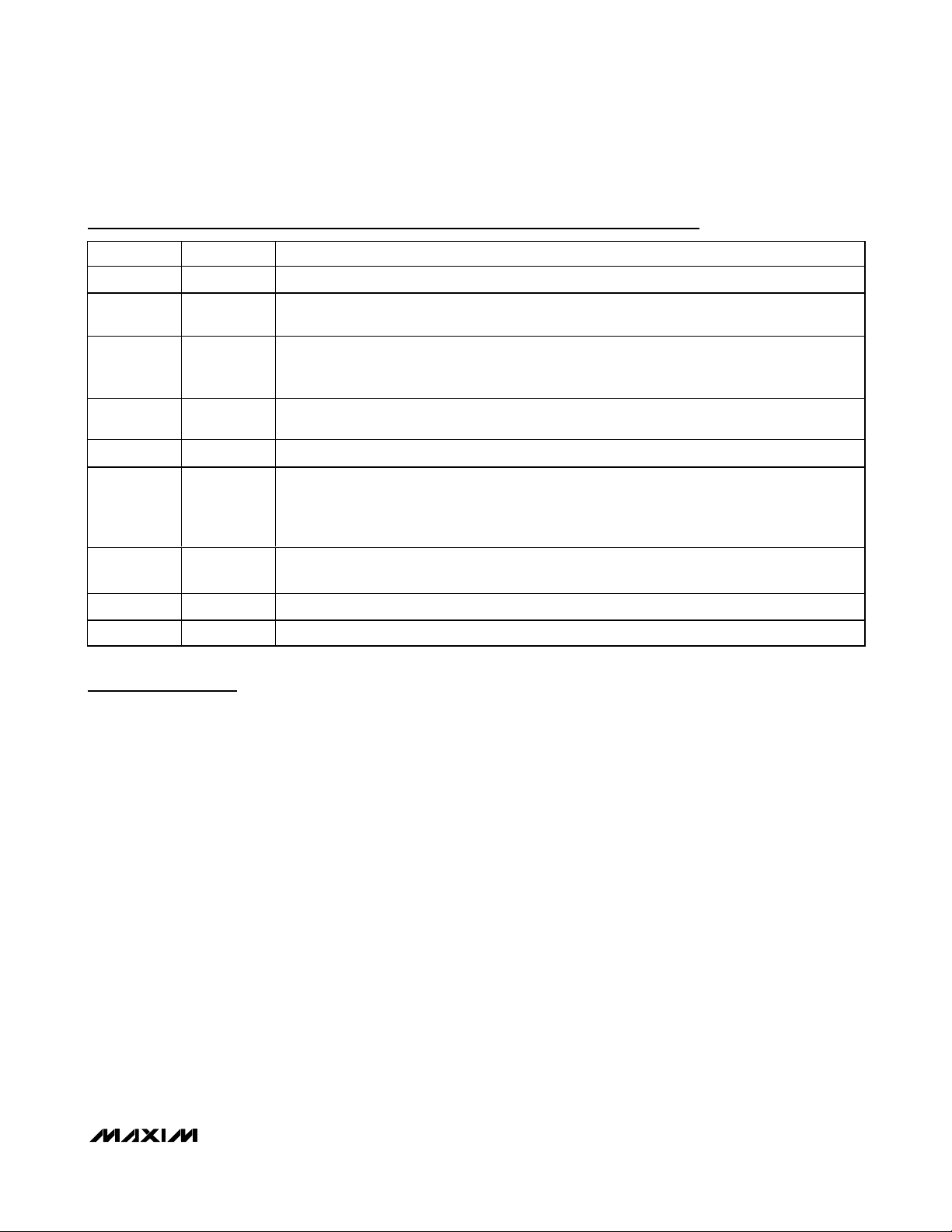
Pin Configuration
19-2227; Rev 2; 3/05
For pricing, delivery, and ordering information, please contact Maxim/Dallas Direct! at
1-888-629-4642, or visit Maxim’s website at www.maxim-ic.com.
Ordering Information
Functional Diagram appears at end of data sheet.
Typical Application appears at end of data sheet.
SPI and QSPI are trademarks of Motorola, Inc.
MICROWIRE is a trademark of National Semiconductor Corp.
*EP = Exposed pad.
EVALUATION KIT
AVAILABLE
PART TEMP RANGE PIN-PACKAGE
MAX6950CEE 0°C to +70°C 16 QSOP-EP*
MAX6950EEE -40°C to +85°C 16 QSOP-EP*
MAX6951CEE 0°C to +70°C 16 QSOP-EP*
MAX6951EEE -40°C to +85°C 16 QSOP-EP*
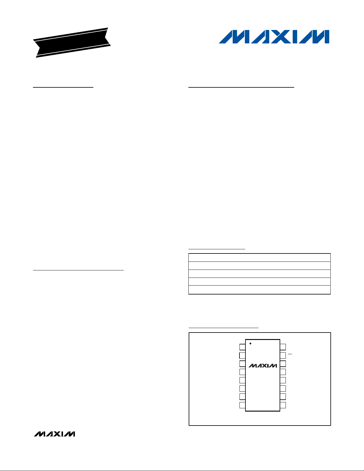
TOP VIEW
1
DIN V+
CLK
2
DIG3/SEG3
DIG2/SEG2
DIG1/SEG1
DIG0/SEG0
ISET
GND
3
MAX6950
4
MAX6951
5
6
7
8
16
15
14
13
12
11
10
9
CS
DIG4/SEG4
(DIG5)/SEG5
(DIG6)/SEG6
(DIG7)/SEG7
SEG8
OSC
( ) MAX6951 ONLY
QSOP
Page 2
MAX6950/MAX6951
Serially Interfaced, +2.7V to +5.5V,
5- and 8-Digit LED Display Drivers
2 _______________________________________________________________________________________
ABSOLUTE MAXIMUM RATINGS
Stresses beyond those listed under “Absolute Maximum Ratings” may cause permanent damage to the device. These are stress ratings only, and functional
operation of the device at these or any other conditions beyond those indicated in the operational sections of the specifications is not implied. Exposure to
absolute maximum rating conditions for extended periods may affect device reliability.
Voltage (with Respect to GND)
V+………………………………. ...................................-0.3V to 6V
All Other Pins................................................-0.3V to (V+ + 0.3V)
DIG1–DIG8 Sink Current.................................................. 440mA
SEG1–SEG9 Source Current.............................................. 55mA
Continuous Power Dissipation (T
A
= +70°C)
16-Pin QSOP (derate 8.34mW/°C above +70°C)........667mW
Operating Temperature Ranges (T
MIN
to T
MAX
)
MAX695_CEE....................................................0°C to +70°C
MAX695_EEE.................................................-40°C to +85°C
Junction Temperature......................................................+150°C
Storage Temperature Range .............................-65°C to +150°C
Lead Temperature (soldering, 10s) .................................+300°C
ELECTRICAL CHARACTERISTICS
(Typical operating circuit, V+ = +3.0V to +5.5V, TA= T
MIN
to T
MAX
, unless otherwise noted.) (Note 1)
PARAMETER SYMBOL CONDITIONS MIN TYP MAX UNITS
Operating Supply Voltage V+ 2.7 5.5 V
Shutdown Supply Current I
Operating Supply Current I+
Master Clock Frequency (OSC
Internal Oscillator)
Master Clock Frequency (OSC
External Clock)
Display Scan Rate (OSC
External Clock)
Display Scan Rate (OSC Internal
Oscillator)
Display Scan Rate (OSC Internal
Oscillator)
OSC Internal/External Detection
Threshold
Dead Clock Protection
Frequency
OSC High Time (OSC External
Clock)
OSC Low Time (OSC External
Clock)
SHDN
f
OSC
f
OSC
f
SCAN
f
SCAN
f
SCAN
V
OSC
f
OSC
t
CH
t
CL
S hutd ow n m od e, al l d i g i tal
i np uts at V + or GN D
All segments on, all digits scanned,
intensity set to full, internal oscillator,
no display load connected
OSC = RC oscillator 1 8
OSC = RC oscillator, R
= 27pF
C
SET
OSC overdriven externally 1 8 MHz
Eight digits scanned, OSC = overdriven
externally
Eight digits scanned, OSC = RC oscillator 155 1250 Hz
Eight digits scanned, OSC = RC oscillator,
R
= 56kΩ, C
SET
Overtemperature 75
T
= +25oC 62 160
A
= 56kΩ,
SET
= 27pF
SET
155 1250 Hz
50 ns
50 ns
10 15 mA
4
625 Hz
1.7 V
75.5 kHz
µA
MHz
Page 3
MAX6950/MAX6951
Serially Interfaced, +2.7V to +5.5V,
5- and 8-Digit LED Display Drivers
_______________________________________________________________________________________ 3
ELECTRICAL CHARACTERISTICS
(Typical operating circuit, V+ = +3.0V to +5.5V, TA= T
MIN
to T
MAX
, unless otherwise noted.) (Note 1)
Note 1: All parameters tested at TA= +25°C. Specifications over temperature are guaranteed by design.
Note 2: Guaranteed by design.
PARAMETER SYMBOL CONDITIONS MIN TYP MAX UNITS
Slow Segment Blink Period
(Internal Oscillator)
Fast Segment Blink Period
(Internal Oscillator)
f
S LOWBLIN K
f
FASTBLIN K
Fast or Slow Segment Blink Duty
Cycle (Note 2)
Digit Drive Sink Current I
Segment Drive Source Current I
Digit Drive Sink Current (Note 2) I
Segment Drive Source Current
(Note 2)
Slew Rate Rise Time ∆I
DIGIT
SEG
DIGIT
I
SEG
SEG
LOGIC INPUTS
Input Current DIN, CLK, CS IIH, I
Logic High Input Voltage DIN,
CLK, CS
Logic Low Input Voltage DIN,
CLK, CS
V
IH
V
IL
H yster esi s V ol tag e D IN , C LK, C S ∆V
TIMING CHARACTERISTICS (Figure 1)
CLK Clock Period t
CLK Pulse Width High t
CLK Pulse Width Low t
C S Fall to CLK Ri se S etup Ti m et
CLK Ri se to CS Rise Hold Time t
DIN Setup Time t
DIN Hold Time t
CS Pulse High t
CP
CH
CL
CSS
CSH
DS
DH
CSW
TIMING CHARACTERISTICS (V+ = +2.7V) (Note 2)
CLK Clock Period t
CLK Pulse Width High t
CLK Pulse Width Low t
C S Fall to CLK Ri se Setup Time t
CLK Ri se to CS Rise Hold Time t
DIN Setup Time t
DIN Hold Time t
CS Pulse High t
CP
CH
CL
CSS
CSH
DS
DH
CSW
Eight digits scanned, OSC = RC oscillator,
R
Eight digits scanned, OSC = RC oscillator,
R
TA = +25°C, V
TA = +25°C, V
TA = +25°C, V+ = 2.7V to 3V, V
TA = +25°C, V+ = 2.7V to 3V, V
/∆tTA = +25°C 35 mA/µs
VIN = 0 or V+ -2 2 µA
IL
I
= 56kΩ, C
SET
= 56kΩ, C
SET
SET
SET
= 27pF
= 27pF
1s
0.5 s
49.9 50 50.1 %
= 2.4V 240 320 400 mA
LED
= 2.4V -30 -40 -50 mA
LED
= 2.2V 80 mA
LED
= 2.2V -10 mA
LED
2.4 V
0.5 V
38.4 ns
19 ns
19 ns
9.5 ns
3ns
9.5 ns
0ns
19 ns
50 ns
24 ns
24 ns
12 ns
4ns
12 ns
4ns
24 ns
0.4 V
Page 4
MAX6950/MAX6951
Serially Interfaced, +2.7V to +5.5V,
5- and 8-Digit LED Display Drivers
4 _______________________________________________________________________________________
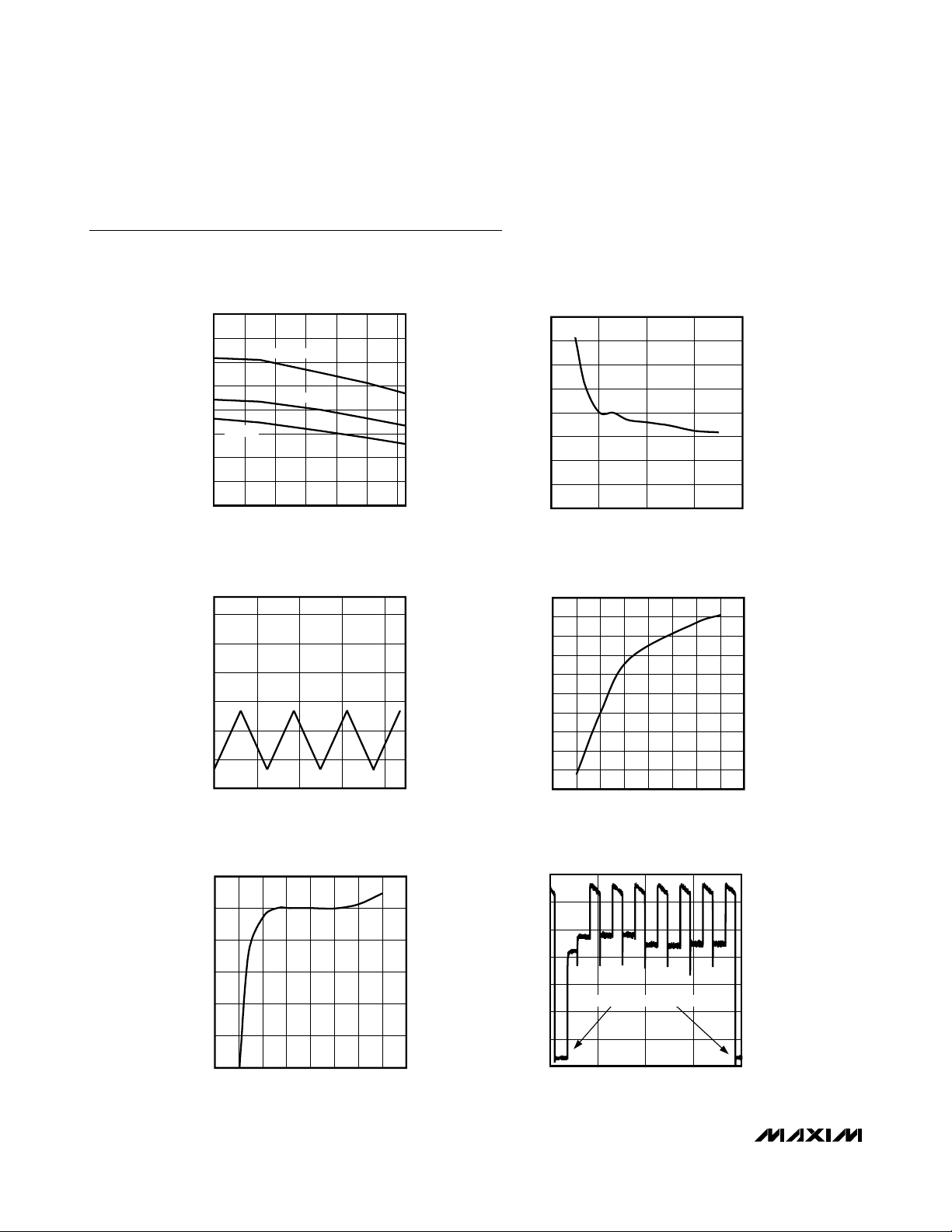
Typical Operating Characteristics
(Typical operating circuit, scan limit set to eight digits, V+ = +3.3V, V
LED
= 2.4V, TA = +25°C, unless otherwise noted.)
INTERNAL OSCILLATOR FREQUENCY
vs. TEMPERATURE
4.40
4.30
4.20
4.10
4.00
3.90
3.80
OSCILLATOR FREQUENCY (MHz)
3.70
3.60
-40 0 20-20
V+ = 2.7V
V+ = 3.3V
V+ = 5V
40
TEMPERATURE (°C)
INTERNAL OSCILLATOR WAVEFORM
AT OSC (PIN 9)
3.0
2.5
2.0
1.5
VOLTAGE AT OSC (V)
1.0
0.5
0
0 400200 600 800
TIMELINE (ns)
60 80
MAX6950/1 toc01
MAX6950/1 toc03
INTERNAL OSCILLATOR FREQUENCY
vs. SUPPLY VOLTAGE
4.40
4.30
4.20
4.10
4.00
3.90
3.80
OSCILLATOR FREQUENCY (MHz)
3.70
3.60
23456
SUPPLY VOLTAGE (V)
DEAD CLOCK OSCILLATOR FREQUENCY
vs. SUPPLY VOLTAGE
80
79
78
77
76
75
74
73
OSCILLATOR FREQUENCY (kHz)
72
71
70
2.0 3.0 3.52.5 4.0 4.5 5.0 5.5 6.0
SUPPLY VOLTAGE (V)
MAX6950/1 toc02
MAX6950/1 toc04
SEGMENT SOURCE CURRENT
vs. SUPPLY VOLTAGE
1.01
1.00
0.99
0.98
0.97
CURRENT NORMALIZED TO 40mA
0.96
0.95
2.0 3.02.5 3.5 4.0 4.5 5.0 5.5 6.0
SUPPLY VOLTAGE (V)
MAX6950/1 toc05
WAVEFORM AT SEGO/DIGO (PIN 6)
V+ = 3.3V, 8 DIGITS SCANNED, 8/16 INTENSITY
3.5
3.0
2.5
2.0
1.5
VOLTAGE (V)
1.0
0.5
0
DIGIT 0 MULTIPLEX TIMESLOT
0 500 1000 1500 2000
TIMELINE (ns)
MAX6950/1 toc06
Page 5
Detailed Description
Differences Between
MAX6950 and MAX6951
The MAX6950 is a five-digit common-cathode display
driver. It drives five digits, with each digit comprising
eight LEDs with cathodes connected to a common
cathode. The display limit is therefore 40 LEDs or digit
segments.
The MAX6951 is an eight-digit common-cathode display driver. It drives eight digits, with each digit comprising eight LEDs. The only difference between the
MAX6950 and MAX6951 is that the MAX6950 is missing
three digit drivers. The MAX6950 can be configured to
scan eight digits, but if the last three digits are wired
up, they do not light.
The MAX6950/MAX6951 use a unique multiplexing
scheme to minimize the connections between the driver
and LED display. The scheme requires that the segment connections are different to each of the five
(MAX6950) or eight (MAX6951) digits (Table 1). This is
shown in the Typical Application Circuit, which uses
single-digit type displays. The MAX6950/MAX6951 are
not intended to drive multidigit display types, which
have the segments internally wired together, unless the
segments are wired with the common cathodes to follow Table 1. The MAX6950/MAX6951 can drive multidigit LED displays that have the segments individually
pinned for each digit because then the digits can be
connected together correctly externally, just as if individual digits were used.
Serial-Addressing Modes
The microprocessor interface on the MAX6950/
MAX6951 is a SPI-compatible 3-wire serial interface
using three input pins (Figure 1). This interface is used
to write configuration and display data to the MAX6950/
MAX6951. The serial interface data word length is 16
bits, which are labeled D15–D0 (Table 2). D15–D8 contain the command address, and D7–D0 contain the
data. The first bit received is D15, the most-significant
bit (MSB). The three input pins are:
• CLK is the serial clock input, and may idle low or
high at the start and end of a write sequence.
• CS is the MAX6950/MAX6951s’ chip-select input,
and must be low to clock data into the MAX6950/
MAX6951.
• DIN is the serial data input, and must be stable
when it is sampled on the rising edge of the clock.
MAX6950/MAX6951
Serially Interfaced, +2.7V to +5.5V,
5- and 8-Digit LED Display Drivers
_______________________________________________________________________________________ 5
Pin Description
PIN NAME FUNCTION
1 DIN Serial Data Input. Data is loaded into the internal 16–bit Shift register on CLK’s rising edge.
2 CLK
3–6, 10–14 DIGX, SEGX
7I
8 GND Ground
9 OSC
15 CS
16 V+ Positive Supply Voltage. Bypass to GND with a 0.1µF capacitor.
PAD E xposed p ad Exposed pad on package underside. Connect to GND.
SET
Serial-Clock Input. On CLK’s rising edge, data is shifted into the Internal Shift register. On CLK’s
falling edge, data is clocked out of DOUT. CLK input is active only while CS is low.
Digit X outputs sink current from the display common cathode when acting as digit drivers.
Segment X drivers source current to the display. Segment/digit drivers are high impedance when
turned off.
Current Setting. Connect to GND through a resistor (R
together with capacitor C
Multiplexer Clock Input. A capacitor (C
multiplex clock is used. Resistor R
together set the multiplex clock frequency. When the external clock is used, OSC should be driven
by a 1MHz to 8MHz clock.
Chip-Select Input. Serial data is loaded into the Shift register while CS is low. The last 16 bits of
serial data are latched on CS’s rising edge.
, also sets the multiplex clock frequency.
SET
) is connected to GND when the internal RC oscillator
SET
(also used to set the peak current) and capacitor C
SET
) to set the peak current. This resistor,
SET
SET
Page 6
MAX6950/MAX6951
The serial interface comprises a 16-bit shift register into
which DIN data is clocked on the rising edge of CLK
when CS is low. When CS is high, transitions on CLK do
not clock data into the shift register. When CS goes
high, the 16 bits in the shift register are parallel loaded
into a 16-bit latch. The 16 bits in the latch are then
decoded to determine and execute the command.
The MAX6950/MAX6951 are written to using the following sequence (Figure 2):
1) Take CLK low.
2) Take CS low. This enables the internal 16-bit shift
register.
3) Clock 16 bits of data in order, D15 first to D0 last,
into DIN, observing the setup and hold times.
4) Take CS high.
CLK and DIN may well be used to transmit data to other
peripherals. The MAX6950/MAX6951 ignore all activity
on CLK and DIN except when CS is low. Data cannot
be read from the MAX6950/MAX6951.
If fewer or greater than 16 bits are clocked into the
MAX6950/MAX6951 between taking CS low and taking
CS high again, the MAX6950/MAX6951 store the last 16
bits received, including the previous transmission(s).
The general case is when n bits (where n > 16) are
transmitted to the MAX6950/MAX6951. The last bits
comprising bits {n-15} to {n} are retained and are parallel loaded into the 16-bit latch as bits D15 to D0,
respectively (Figure 3).
Digit and Control Registers
Table 3 lists the addressable Digit and Configuration
registers. The digit registers are implemented by two
planes of 8-byte dual-port SRAM, P0 and P1.
Initial Power-Up
On initial power-up, all control registers are reset, the
display is blanked, and the MAX6950/MAX6951 enter
shutdown mode. Program the display driver prior to display use. Otherwise, it is initially set to scan five digits, it
does not decode data in the data registers, and the
Intensity register is set to its minimum value. Table 4
lists the register status after power-up.
Configuration Register
The configuration register is used to enter and exit shutdown, select the blink rate, globally enable and disable
the blink function, globally clear the digit data, and
reset the blink timing. Bit position D1 should always be
written with a zero when the configuration register is
updated. See Table 5 for configuration register format.
The S bit selects shutdown or normal operation.
The B bit selects the blink rate.
The E bit globally enables or disables the blink function.
The T bit resets the blink timing.
The R bit globally clears the digit data for both planes
P0 and P1 for all digits.
When the MAX6950/MAX6951 are in shutdown mode
(Table 6), the scan oscillator is halted; all segment and
digit drivers are high impedance. Data in the digit and
Serially Interfaced, +2.7V to +5.5V,
5- and 8-Digit LED Display Drivers
6 _______________________________________________________________________________________
Table 1. Standard Driver Connection to Single-Digit Displays
Table 2. Serial-Data Format (16 Bits)
DIG/SEG0
PIN 6
LED Digit 0 CC0 SEG dp SEG g SEG f SEG e SEG d SEG c SEG b SEG a
LED Digit 1 SEG dp CC1 SEG g SEG f SEG e SEG d SEG c SEG b SEG a
LED Digit 2 SEG dp SEG g CC2 SEG f SEG e SEG d SEG c SEG b SEG a
LED Digit 3 SEG dp SEG g SEG f CC3 SEG e SEG d SEG c SEG b SEG a
LED Digit 4 SEG dp SEG g SEG f SEG e CC4 SEG d SEG c SEG b SEG a
LED Digit 5 SEG dp SEG g SEG f SEG e SEG d CC5 SEG c SEG b SEG a
LED Digit 6 SEG dp SEG g SEG f SEG e SEG d SEG c CC6 SEG b SEG a
LED Digit 7 SEG dp SEG g SEG f SEG e SEG d SEG c SEG b CC7 SEG a
D15 D14 D13 D12 D11 D10 D9 D8 D7 D6 D5 D4 D3 D2 D1 D0
DIG/SEG1
PIN 5
ADDRESS MSB DATA LSB
DIG/SEG2
PIN 4
DIG/SEG3
PIN 3
DIG/SEG4
PIN 14
DIG/SEG5
PIN 13
DIG/SEG6
PIN 12
DIG/SEG7
PIN 11
SEG 8
PIN 10
Page 7

control registers remains unaltered. Shutdown can be
used to save power. For minimum supply current in
shutdown mode, logic inputs should be at ground or
V+ (CMOS-logic levels). The display driver can be programmed while in shutdown mode, and shutdown
mode can be overridden by the display test function.
Table 7 lists the blink rate selection format.
If blink is globally enabled by setting the E bit of the
configuration register (Table 8), then the digit data in
both planes P0 and P1 are used to control the display
(Table 9).
When the global blink timing synchronization bit is set,
the multiplex and blink timing counter is cleared on the
rising edge of CS. By setting the T bit in multiple
MAX6950/MAX6951s at the same time (or in quick succession), the blink timing can be synchronized across
all the devices.
When the global digit data clear (R data bit D5) is set,
the digit data for both planes P0 and P1 for ALL digits
is cleared on the rising edge of CS. Digits with decode
enabled display the zero. Digits without decode
enabled show all segments unlit.
MAX6950/MAX6951
Serially Interfaced, +2.7V to +5.5V,
5- and 8-Digit LED Display Drivers
_______________________________________________________________________________________ 7
Figure 1. Timing Diagram
Figure 2. Transmission of 16 Bits to the MAX6950/MAX6951
Figure 3 . Transmission of More than 16 Bits to the MAX6950/MAX6951
t
CS
CSW
t
CLtCH
D14 D1 D0
CLK
DIN
t
CSS
t
DH
t
DS
D15
CS
CLK
DIN
D15 D14
D13
D12
D11 D10
D9
CS
t
D5
CSH
D4 D3 D2
D1
D0
t
CP
D8
D6
D7
CLK
N-11
BIT1
BIT2 N-15
DIN
N-14
N-13 N-12
N-10
N-9
N-8
N-7
N-6 N-5 N-4
N-3
N-2
N-1 N
Page 8

MAX6950/MAX6951
No-Op Register
The no-op register is used when the MAX6950/
MAX6951 are connected as the last device on a chain
of cascaded SPI devices. To write the other cascaded
device(s), ensure that while the intended device
receives its specific command, the MAX6950/MAX6951
receive a no-op command.
Display-Test Register
The display-test register switches the drivers between
one of two modes: normal and display test. Display-test
mode turns all LEDs on by overriding, but not altering,
all control and digit registers (including the Shutdown
register) In display-test mode, eight digits are scanned
and the duty cycle is 7/16 (half power). Table 11 lists
the display-test register format.
Serially Interfaced, +2.7V to +5.5V,
5- and 8-Digit LED Display Drivers
8 _______________________________________________________________________________________
Table 3. Register Address Map
REGISTER
No-Op 0 0 0 0 0 0 0 0 0x00
Decode Mode 0 0 0 0 0 0 0 1 0x01
Intensity 0 0 0 0 0 0 1 0 0x02
Scan Limit 0 0 0 0 0 0 1 1 0x03
Configuration 0 0 0 0 0 1 0 0 0x04
Factory reserved. Do not write to this.
Display Test 0 0 0 0 0 1 1 1 0x07
Digit 0 plane P0 only (plane 1 unchanged) 0 0 1 0 0 0 0 0 0x20
Digit 1 plane P0 only (plane 1 unchanged) 0 0 1 0 0 0 0 1 0x21
Digit 2 plane P0 only (plane 1 unchanged) 0 0 1 0 0 0 1 0 0x22
Digit 3 plane P0 only (plane 1 unchanged) 0 0 1 0 0 0 1 1 0x23
Digit 4 plane P0 only (plane 1 unchanged) 0 0 1 0 0 1 0 0 0x24
Digit 5 plane P0 only (plane 1 unchanged) 0 0 1 0 0 1 0 1 0x25
Digit 6 plane P0 only (plane 1 unchanged) 0 0 1 0 0 1 1 0 0x26
Digit 7 plane P0 only (plane 1 unchanged) 0 0 1 0 0 1 1 1 0x27
Digit 0 plane P1 only (plane 0 unchanged) 0 1 0 0 0 0 0 0 0x40
Digit 1 plane P1 only (plane 0 unchanged) 0 1 0 0 0 0 0 1 0x41
Digit 2 plane P1 only (plane 0 unchanged) 0 1 0 0 0 0 1 0 0x42
Digit 3 plane P1 only (plane 0 unchanged) 0 1 0 0 0 0 1 1 0x43
Digit 4 plane P1 only (plane 0 unchanged) 0 1 0 0 0 1 0 0 0x44
Digit 5 plane P1 only (plane 0 unchanged) 0 1 0 0 0 1 0 1 0x45
Digit 6 plane P1 only (plane 0 unchanged) 0 1 0 0 0 1 1 0 0x46
Digit 7 plane P1 only (plane 0 unchanged) 0 1 0 0 0 1 1 1 0x47
D i g i t 0 p l ane P 0 and p l ane P 1 ( w i th sam e d ata) 0 1 1 0 0 0 0 0 0x60
D i g i t 1 p l ane P 0 and p l ane P 1 ( w i th sam e d ata) 0 1 1 0 0 0 0 1 0x61
D i g i t 2 p l ane P 0 and p l ane P 1 ( w i th sam e d ata) 0 1 1 0 0 0 1 0 0x62
D i g i t 3 p l ane P 0 and p l ane P 1 ( w i th sam e d ata) 0 1 1 0 0 0 1 1 0x63
D i g i t 4 p l ane P 0 and p l ane P 1 ( w i th sam e d ata) 0 1 1 0 0 1 0 0 0x64
D i g i t 5 p l ane P 0 and p l ane P 1 ( w i th sam e d ata) 0 1 1 0 0 1 0 1 0x65
D i g i t 6 p l ane P 0 and p l ane P 1 ( w i th sam e d ata) 0 1 1 0 0 1 1 0 0x66
D i g i t 7 p l ane P 0 and p l ane P 1 ( w i th sam e d ata) 0 1 1 0 0 1 1 1 0x67
D15 D14 D13 D12 D11 D10 D9 D8
0 0 0 0 0 1 1 0 0x06
COMMAND ADDRESS
HEX
CODE
Page 9

Scan-Limit Register
The scan-limit register sets how many digits are displayed, from one to eight digits. It is possible to set the
MAX6950 (the five-digit part) to scan six, seven, or
eight digits. The MAX6951 set to eight digits displays
five digits less brightly than if it had been set to scan
five digits, but the brightness would match that of a
MAX6951 used in the same system if the Intensity registers are set to the same value. For example, consider
an 11-digit requirement. This can be served by using a
MAX6950 to drive five digits plus a MAX6951 to drive
six digits. Both parts are configured to drive six digits to
ensure the brightness is the same.
The digits are displayed in a multiplexed manner with a
typical display scan rate of 1kHz with five digits displayed or 625Hz with eight digits displayed with f
OSC
=
4MHz. Since the number of scanned digits affects the
display brightness, the Scan-Limit register should not
be used to blank portions of the display (such as for
leading-zero suppression). Table 12 lists the scan-limit
register format.
Intensity Register
Digital control of display brightness is provided by an
internal pulse-width modulator, which is controlled by the
lower nibble of the intensity register (Figure 4). The modulator scales the average segment current in 16 steps
from a minimum of 15/16 down to 1/16 of the peak current. The minimum interdigit blanking time is set to 1/16
of a cycle. See Table 13 for Intensity register format.
Decode Mode Register
The decode mode register sets hexadecimal code
(0–9, A–F) or no-decode operation for each digit. Each
bit in the register corresponds to one digit. A logic high
selects hexadecimal code font decoding for that digit,
while logic low bypasses the decoder. Digits may be
set for decode or no-decode in any combination.
Examples of the decode mode control register format
are shown in Table 14.
When the hexadecimal code-decode mode is used, the
decoder looks only at the lower nibble of the data in the
digit register (D3–D0), disregarding bits D6–D4. D7,
which sets the decimal point (SEG DP), is independent
of the decoder, and is positive logic (D7 = 1 turns the
decimal point on). Table 15 lists the hexadecimal code
font. When no-decode is selected, data bits D7–D0 correspond to the segment lines of the MAX6950/
MAX6951. Table 15 shows the one-to-one pairing of
each data bit to the appropriate segment line.
Display Digit Registers
The MAX6950/MAX6951 use a digit register to store the
data that the user wishes to display on the LED digits.
These digit registers are implemented by two planes of
8-byte, dual-port SRAM, called P0 and P1. The digit
registers are dual port to enable them to be written to
through the SPI interface, asynchronous to being read
to multiplex the display.
MAX6950/MAX6951
Serially Interfaced, +2.7V to +5.5V,
5- and 8-Digit LED Display Drivers
_______________________________________________________________________________________ 9
Table 4. Initial Power-Up Register Status
(
)
REGISTER POWER-UP CONDITION
Decode
Intensity 1/16 (min on) 0x02 X X X X 0 0 0 0
Scan Limit Display 5 digits: 0 1 2 3 4 0x03 X X X X X 1 0 0
Configuration
Display Test Normal operation 0x07 X X X X X X X 0
Digit 0 Blank digit, both planes 0x60 0 0 0 0 0 0 0 0
Digit 1 Blank digit, both planes 0x61 0 0 0 0 0 0 0 0
Digit 2 Blank digit, both planes 0x62 0 0 0 0 0 0 0 0
Digit 3 Blank digit, both planes 0x63 0 0 0 0 0 0 0 0
Digit 4 Blank digit, both planes 0x64 0 0 0 0 0 0 0 0
Digit 5 Blank digit, both planes 0x65 0 0 0 0 0 0 0 0
Digit 6 Blank digit, both planes 0x66 0 0 0 0 0 0 0 0
Digit 7 Blank digit, both planes 0x67 0 0 0 0 0 0 0 0
No decode for digits 7–0 0x01 0 0 0 0 0 0 0 0
S hutd ow n enab l ed /b l i nk
sp eed i s sl ow /b l i nk d i sab l ed
ADDRESS
HEX
CODE
0x04 X X X 0 0 0 0 0
D7 D6 D5 D4 D3 D2 D1 D0
REGISTER DATA
Page 10

MAX6950/MAX6951
Each LED digit is represented by 2 bytes of memory, 1
byte in plane P0 and the other in plane P1. Each LED
digit’s segment is represented by 2 bits of memory, 1
bit from the appropriate byte in each plane. The digit
registers are mapped so that a digit’s data can be
updated in plane P0, or plane P1, or both planes at the
same time (Table 3).
Serially Interfaced, +2.7V to +5.5V,
5- and 8-Digit LED Display Drivers
10 ______________________________________________________________________________________
Table 5. Configuration Register Format
(
)
Table 6. Shutdown Control (S Data Bit D0) Format
(
)
Table 7. Blink Rate Selection (B Data Bit D2) Format
(
)
Table 8. Global Blink Enable/Disable (E Data Bit D3) Format
(
)
Table 9. Global Blink Timing Synchronization (T Data Bit D4) Format
(
)
MODE
Configuration register 0x04 X X R T E B 0 S
ADDRESS
CODE
HEX
D7 D6 D5 D4 D3 D2 D1 D0
MODE
Shutdown 0x04 X X R T E B 0 0
Normal operation 0x04 X X R T E B 0 1
ADDRESS
CODE
HEX
D7 D6 D5 D4 D3 D2 D1 D0
MODE
S l ow - b l i nki ng seg m ents
b l i nk on for 1s, off for 1s
w i th f
Fast-blinking segments
blink on for 0.5s, off for
0.5s with f
OS C
= 4M H z
= 4MHz
OSC
ADDRESS
HEX
CODE
0x04 X X R T E 0 0 S
0x04 X X R T E 1 0 S
D7 D6 D5 D4 D3 D2 D1 D0
REGISTER DATA
REGISTER DATA
REGISTER DATA
MODE
Blink function is
disabled
Blink function is
enabled
ADDRESS
CODE
HEX
0x04 X X R T 0 B 0 S
0x04 X X R T 1 B 0 S
D7 D6 D5 D4 D3 D2 D1 D0
REGISTER DATA
MODE
Blink timing counters
are unaffected
Blink timing counters
are cleared on the
rising edge of CS
ADDRESS
CODE
HEX
0x04 X X R 0 E B 0 S
0x04 X X R 1 E B 0 S
D7 D6 D5 D4 D3 D2 D1 D0
REGISTER DATA
Page 11

If the blink function is disabled through the Blink Enable
Bit E (Table 8) in the configuration register, then the digit
register data in plane P0 is used to multiplex the display.
The digit register data in P1 is not used (Table 17).
If the blink function is enabled, then the digit register
data in both plane P0 and plane P1 are alternately used
to multiplex the display. Blinking is achieved by multiplexing the LED display using data plane P0 and plane
P1 on alternate phases of the blink clock (Table 18).
Display Blink Mode
The display blinking facility, when enabled, makes the
driver flip automatically between displaying the digit
register data in planes P0 and plane P1. If the digit register data for any individual segment is different in the
two planes, then that segment appears to blink or flash
on and off. Once blinking has been configured, it continues automatically without further intervention.
Blink Speed
The blink speed is determined by frequency of the multiplex clock, OSC, and by the setting of the Blink Rate
Selection Bit B (Table 7) in the configuration register.
The Blink Rate Selection Bit B sets either fast or slow
blink speed for the whole display.
Multiplex Clock and OSC Oscillator
The OSC input pin is used to set both the display scan
rate and the blink timing for the display driver. OSC
must either be fitted with an external capacitor C
SET
to
GND to set the frequency of the MAX6950/MAX6951s’
internal RC oscillator, or be overdriven with an external
TTL/CMOS clock.
MAX6950/MAX6951
Serially Interfaced, +2.7V to +5.5V,
5- and 8-Digit LED Display Drivers
______________________________________________________________________________________ 11
Table 10. Global Clear Digit Data (R Data Bit D5) Format
(
)
Table 11. Display-Test Register Format
(
)
Table 12. Scan-Limit Register Format
(
)
MODE
Digit data for both
planes P0 and P1 are
unaffected
Digit data for both
planes P0 and P1 are
cleared on the rising
edge of CS
ADDRESS
CODE
HEX
0x04 X X 0 T E B 0 S
0x04 X X 1 T E B 0 S
D7 D6 D5 D4 D3 D2 D1 D0
REGISTER DATA
MODE
Normal operation 0x07 X XXXXXX0
Display test 0x07 X XXXXXX1
ADDRESS
CODE
HEX
D7 D6 D5 D4 D3 D2 D1 D0
REGISTER DATA
SCAN LIMIT
Display digit 0 only 0x03 X X X X X 0 0 0 0xX0
Display digits 0 and 1 0x03 X X X X X 0 0 1 0xX1
Display digits 0 and 1 2 0x03 X X X X X 0 1 0 0xX2
Display digits 0 and 1 2 3 0x03 X X X X X 0 1 1 0xX3
Display digits 0 and 1 2 3 4 0x03 X X X X X 1 0 0 0xX4
Display digits 0 and 1 2 3 4 5 0x03 X X X X X 1 0 1 0xX5
Display digits 0 and 1 2 3 4 5 6 0x03 X X X X X 1 1 0 0xX6
Display digits 0 and 1 2 3 4 5 6 7 0x03 X X X X X 1 1 1 0xX7
ADDRESS
CODE
HEX
D7 D6 D5 D4 D3 D2 D1 D0
REGISTER DATA
HEX
CODE
Page 12

MAX6950/MAX6951
The allowed range of the frequency at the OSC pin, f
OSC
,
is 1MHz to 8MHz, which allows the blink frequency to be
adjusted over a wide range. The internal oscillator may
be accurate enough for many applications using a single
device. If an exact or synchronized blink rate is required,
then OSC should be driven by an external clock.
The display scan rate (defined in the Electrical
Characteristics table) is calculated by dividing f
OSC
by
4000 for the MAX6950 (scanning a full five digits), or by
6400 for the MAX6951 (scanning a full eight digits). The
display scan rate is the refresh rate for all the digits of the
display. With f
OSC
at 4MHz, each display digit is enabled
for 200µs.
There is a fail-safe circuit in the MAX6950/MAX6951 to
ensure the display multiplexing works if the OSC is configured incorrectly. This ensures that the driver cannot
remain stuck on a single digit, forcing a peak current continuously through segments. The fail-safe circuit detects
that f
OSC
is too slow, and generates extra clock transi-
tions to guarantee a minimum effective clock of typically
75.5kHz. The scan rate for eight digits is about 11Hz in
fail-safe mode, and appears to flicker to most observers.
A flickering display is a good indication that there is a
problem with the multiplex clock. The clock failure detection works regardless of the clock source being the internal RC oscillator or external clock drive.
The RC oscillator uses an external resistor R
SET
(which
also sets the peak segment current) and an external
capacitor C
SET
to set the oscillator frequency. The rec-
ommended values of R
SET
and C
SET
set the oscillator at
4MHz, which makes the slow and fast blink frequency
0.5Hz and 1Hz, respectively.
Synchronization of Blinking Across
Multiple MAX6950/MAX6951 Drivers
The OSC inputs of multiple MAX6950/MAX6951 drivers
can be connected together to an external clock to make
the devices blink at the same frequency. Segment blinking may be synchronized across multiple MAX6950/
MAX6951s so that all drivers blink not only at the same
frequency, but also in phase. When the control register is
written with the T bit set (Table 9), the OSC divider chain
is cleared and the display multiplexing sequence reset.
To synchronize several drivers, it is necessary to write
this register in all drivers at the same time. In practice,
adequate synchronization can be achieved by writing to
multiple drivers in quick succession.
When the global blink timing synchronization bit is set,
the multiplexing and blink counter is cleared on the rising edge of CS. By setting the T bit in multiple
MAX6950/MAX6951s at the same time (or in quick succession), the blink timing can be synchronized across
all the devices. Note that the display multiplexing
Serially Interfaced, +2.7V to +5.5V,
5- and 8-Digit LED Display Drivers
12 ______________________________________________________________________________________
Table 13. Intensity Register Format
(
)
DUTY CYCLE
1/16 (min on) 2.5 0x02 X X X X 00000xX0
2/16 5 0x02 X X X X 00010xX1
3/16 7.5 0x02 X X X X 00100xX2
4/16 10 0x02 X X X X 00110xX3
5/16 12.5 0x02 X X X X 01000xX4
6/16 15 0x02 X X X X 01010xX5
7/16 17.5 0x02 X X X X 01100xX6
8/16 20 0x02 X X X X 01110xX7
9/16 22.5 0x02 X X X X 10000xX8
10/16 25 0x02 X X X X 10010xX9
11/16 27.5 0x02 X X X X 10100xXA
12/16 30 0x02 X X X X 10110xXB
13/16 32.5 0x02 X X X X 11000xXC
14/16 35 0x02 X X X X 11010xXD
15/16 37.5 0x02 X X X X 11100xXE
15/16 (max on) 37.5 0x02 X X X X 11110xXF
TYPICAL SEGMENT
CURRENT (mA)
ADDRESS
CODE
HEX
D7 D6 D5 D4 D3 D2 D1 D0
HEX
CODE
Page 13

MAX6950/MAX6951
Serially Interfaced, +2.7V to +5.5V,
5- and 8-Digit LED Display Drivers
______________________________________________________________________________________ 13
Figure 4. Multiplex and Intensity Timing Diagram
DIGIT CATHODE
DRIVER INTENSITY
SETTINGS
1/16TH
(MIN ON)
ANODE
MIN ON
HIGH-Z
2/16TH
3/16TH
13/16TH
14/16TH
15/16TH
16/16TH
MAX ON
200µs TIME SLOT
DIGIT 0
200µs TIME SLOT
DIGIT 1
LOW
CURRENT SOURCE ENABLED
HIGH-Z
LOW
LOW
LOW
LOW
LOW
LOW
200µs TIME SLOT
HIGH-Z
ONE COMPLETE 1.6ms MULTIPLEX CYCLE AROUND 8 DIGITS
DIGIT 2
200µs TIME SLOT
DIGIT 3
DIGIT 0's 200µs MULTIPLEX TIME SLOT
HIGH-Z
HIGH-Z
200µs TIME SLOT
DIGIT 4
200µs TIME SLOT
DIGIT 5
200µs TIME SLOT
DIGIT 6
HIGH-Z
200µs TIME SLOT
DIGIT 7
HIGH-Z
HIGH-Z
HIGH-Z
START OF NEXT
200µs TIME SLOT
DIGIT 0
CYCLE
CURRENT SOURCE ENABLED
ANODE
MAX ON
HIGH-Z
ANODE (UNLIT)
HIGH-Z
MINIMUM 12.5µs INTERDIGIT BLANKING INTERVAL
HIGH-Z
HIGH-Z
Page 14

MAX6950/MAX6951
sequence is also reset, which might give rise to a onetime display flicker when the register is written.
Selecting External Components R
SET
and C
SET
to Set Oscillator Frequency
and Segment Current
The RC oscillator uses an external resistor R
SET
and an
external capacitor C
SET
to set the oscillator frequency,
f
OSC
. The allowed range of f
OSC
is 1MHz to 8MHz.
R
SET
also sets the peak segment current. The recom-
mended values of R
SET
and C
SET
set the oscillator to
4MHz, which makes the blink frequencies 0.5Hz and
1Hz. The recommended value of R
SET
also sets the
peak current to 40mA, which makes the segment current adjustable from 2.5mA to 37.5mA in 2.5mA steps.
I
SEG
= KI/ R
SET
mA
f
OSC
= KF/ (R
SET
✕
C
SET
+ C
STRAY
) MHz
Where:
KI= 2240
Serially Interfaced, +2.7V to +5.5V,
5- and 8-Digit LED Display Drivers
14 ______________________________________________________________________________________
Table 14. Decode-Mode Register Examples
(
)
Table 15. Hexadecimal Font
The decimal point segment is lit when bit D7 = 1.
DECODE CODE
No decode for digits 7–0 0x01 0 0 0 0 0 0 0 0 0x00
Hexadecimal decode for digit 0,
no decode for digits 7–1
Hexadecimal decode for digits
2–0, no decode for digits 7–3
Hexadecimal decode for digits
7–0
ADDRESS
CODE
HEX
0x01 0 0 0 0 0 0 0 1 0x01
0x01 0 0 0 0 0 1 1 1 0x07
0x01 1 1 1 1 1 1 1 1 0xFF
D7 D6 D5 D4 D3 D2 D1 D0
7-SEGMENT
CHARACTER
0 X 0000 1111110
1 X 0001 0110000
2 X 0010 1101101
3 X 0011 1111001
4 X 0100 0110011
5 X 0101 1011011
6 X 0110 1011111
7 X 0111 1110000
8 X 1000 1111111
9 X 1001 1111011
A X 1010 1110111
B X 1011 0011111
C X 1100 1001110
D X 1101 0111111
E X 1110 1001111
F X 1111 1000111
D7* D 6 – D 4 D3 D2 D1 D0 dp* a b c d e f g
REGISTER DATA ON SEGMENTS = 1
REGISTER DATA
HEX
CODE
Page 15

KF= 6720
R
SET
= external resistor in kΩ
C
SET
= external capacitor in pF
C
STRAY
= stray capacitance from OSC pin to GND in
pF, typically 3pF
The recommended value of R
SET
is 56kΩ and the rec-
ommended value of C
SET
is 27pF.
The recommended value of R
SET
is the minimum
allowed value, since it sets the display driver to the
maximum allowed segment current. R
SET
can be set to
a higher value to set the segment current to a lower
peak value where desired. The user must also ensure
that the peak current specifications of the LEDs connected to the driver are not exceeded.
The effective value of C
SET
includes not only the actual
external capacitor used, but also the stray capacitance
from the OSC pin to GND. This capacitance is usually
in the 1pF to 5pF range, depending on the layout used.
LED Maximum Reverse Voltage
The display connection scheme used by the
MAX6950/MAX6951 puts LED segments in reverse bias
during a portion of the multiplexing time. The maximum
applied reverse bias voltage is the value of the supply
voltage, V+. It is therefore important to ensure that the
LEDs chosen are rated to withstand a reverse bias
equal to the maximum supply voltage applied to the
MAX6950/MAX6951.
Applications Information
Choosing Supply Voltage to Minimize
Power Dissipation
The MAX6950/MAX6951 drive a peak current of 40mA
into LEDs with a 2.4V forward-voltage drop when operated from a supply voltage of at least 3.0V. The minimum voltage drop across the internal LED drivers is
therefore (3.0V - 2.4V) = 0.6V. If a higher supply voltage is used, the driver absorbs a higher voltage, and
the driver’s power dissipation increases accordingly.
However, if the LEDs used have a higher forward voltage drop than 2.4V, the supply voltage must be raised
accordingly to ensure that the driver always has at least
0.6V headroom.
The voltage drop across the drivers with a nominal +5V
supply (5.0V - 2.4V) = 2.6V is nearly 3 times the drop
across the drivers with a nominal 3.3V supply (3.3V -
2.4V) = 0.9V. In many systems, consumption is an
important design criterion, and the MAX6950/MAX6951
should be operated from the system’s 3.3V nominal
supply. In other designs, the lowest supply voltage may
be 5V. The issue now is to ensure the dissipation limit
for the MAX6950/MAX6951 is not exceeded. This can
be achieved by inserting a series resistor in the supply
to the MAX6950/MAX6951, ensuring that the supply
decoupling capacitors are still on the MAX6950/
MAX6951 side of the resistor. For example, consider
the requirement that the minimum supply voltage to a
MAX6951 must be 3.0V, and the input supply range is
5V ±5%. Maximum supply current is 15mA + (40mA
✕
8) = 335mA. Minimum input supply voltage is 4.75V.
Maximum series resistor value is (4.75V - 3.0V)/0.335A
= 5.2Ω. We choose 4.7Ω ±10%. Worst-case resistor
dissipation is at maximum toleranced resistance, i.e.,
(0.335A)
2
✕
(4.7Ω✕1.1) = 0.584W. We choose a 1W
resistor rating. The maximum MAX6951 supply voltage
is at maximum input supply voltage and minimum toleranced resistance, i.e., 5.25V - (0.335A ✕4.7Ω✕0.9) =
3.83V.
Low-Voltage Operation
The MAX6950/MAX6951 work over the +2.7V to +5.5V
supply range. The minimum useful supply voltage is
determined by the forward voltage drop of the LEDs at
the peak current I
SEG
, plus the 0.6V headroom required
by the driver output stages. The MAX6950/MAX6951
correctly regulate I
SEG
with a supply above this minimum voltage. If the supply drops below this minimum
voltage, the driver output stages may brown out, and
MAX6950/MAX6951
Serially Interfaced, +2.7V to +5.5V,
5- and 8-Digit LED Display Drivers
______________________________________________________________________________________ 15
Table 16. No-Decode Mode Data Bits and
Corresponding Segment Lines
REGISTER DATA
D7 D6 D5 D4 D3 D2 D1 D0
Segment line dp a b c d e f g
a
bf
g
ce
d
d
Page 16

MAX6950/MAX6951
be unable to regulate the current correctly. As the supply voltage drops further, the LED segment drive current becomes effectively limited by the output drivers'
on-resistance, and the LED drive current drops. The
characteristics of each individual LED in a modern 7segment digit usually match well, so the result is that
the display intensity dims uniformly as supply voltage
drops out of regulation and beyond. The MAX6950/
MAX6951 operate down to 2V supply voltage (although
most displays are very dim at this voltage), providing
that the MAX6950/MAX6951 are powered up initially to
at least 2.7V to trigger the device's internal reset, and
also that the SPI interface is constrained to 5Mbps.
Computing Power Dissipation
The upper limit for power dissipation (PD) for the
MAX6950/MAX6951 is determined from the following
equation:
P
D
= (V+ x I+) + (V+ - V
LED
) (DUTY ✕I
SEG
✕
N)
Where:
V+ = supply voltage
DUTY = duty cycle set by intensity register
N = number of segment driven (worst case is 8)
V
LED
= LED forward voltage
I
SEG
= segment current set by R
SET
PD = power dissipation, in mW if currents are in mA
Dissipation example:
I
SEG
= 40mA, N = 8, Duty = 15/16, V
LED
= 2.4V at
40mA, V+ = 3.6V
PD= 3.6V (15mA) + (3.6V - 2.4V)(15 / 16 ✕40mA x 8)
= 0.414W
Thus, for the 16-pin QSOP package (TJA= 1/0.00834 =
+120°C/W), the maximum allowed ambient temperature
TAis given by:
T
J (MAX)
= TA+ (P
D
✕
TJA) = +150°C = TA+ (0.44
✕
+120°C/W)
So TA= +100°C. Thus, the device can be operated
safely at a maximum package temperature of +85°C.
Power Supplies
The MAX6950/MAX6951 operate from a single +2.7V to
+5.5V power supply. Bypass the power supply to
ground with a 0.1µF capacitor as close to the pin as
possible. Add a 22µF capacitor if the MAX6950/
MAX6951 are not close to the board’s input bulk decoupling capacitor.
Connect the underside exposed pad to GND.
Board Layout
When designing a board, use the following guidelines:
1. The R
SET
connection to pin 7 is a high-impedance
node, and sensitive to layout. Place R
SET
right next
to pins 7 and 8 and route R
SET
directly to these pins
with very short tracks.
2. Ensure that the track from the ground end of R
SET
routes directly to pin 8, and that this track is not
used as part of any other ground connection.
Figure 5 shows a good layout. The decoupling capacitors C1 (ceramic) and C2 (bulk, if required) are located
above the IC. The ground track to R
SET
is a separate
track from both the IC's power ground connection and
the ground plane.
Serially Interfaced, +2.7V to +5.5V,
5- and 8-Digit LED Display Drivers
16 ______________________________________________________________________________________
Table 17. Digit Register Mapping with
Blink Globally Disabled
Table 18. Digit Register Mapping with
Blink Globally Enabled
SEGMENT’S
BIT SETTING
IN PLANE P1
X0
X1
SEGMENT’S
BIT SETTING
IN PLANE P0
SEGMENT
BEHAVIOR
Segment off during both
halves of each blink
period
Segment off during both
halves of each blink
period
SEGMENT’S
BIT SETTING
IN PLANE P1
0 0 Segment off
01
10
1 1 Segment on
SEGMENT’S
BIT SETTING
IN PLANE P0
SEGMENT
BEHAVIOR
Segment on only during
the 1st half of each blink
period
Segment on only during
the 2nd half of each blink
period
Page 17

Chip Information
TRANSISTOR COUNT: 17,350
PROCESS: CMOS
MAX6950/MAX6951
Serially Interfaced, +2.7V to +5.5V,
5- and 8-Digit LED Display Drivers
______________________________________________________________________________________ 17
Typical Application Circuit
Figure 5. Sample Board Layout
3.3V
C2
22µF
µC
DIN
CS
CLK
1
DIN
15
CS
2
CLK
16
MAX6951
8
DIG1–DIG8
SEG1–SEG9
ISET
OSC
C1
100nF
9
8 DIGITS
AND SEGMENTS
(SEE TABLE 1 FOR CONNECTIONS)
7
R
SET
9
C
SET
27pF
56kΩ
Page 18

MAX6950/MAX6951
Serially Interfaced, +2.7V to +5.5V,
5- and 8-Digit LED Display Drivers
18 ______________________________________________________________________________________
Functional Diagram
ISET
OSC
SEGMENT
CURRENT
REFERENCE
MULTIPLEX, PWM BLINK
COUNTERS
HEXADECIMAL
ROM
MODEIN
8
OUT
3
PWM
BRIGHTNESS
CONTROL
DIGIT
MULTIPLEXER
8 CATHODE DRIVERS
9 ANODE DRIVERS
DIG0/SEG0
DIG1/SEG1
DIG2/SEG2
PWM
DIGIT
DIG3/SEG3
DIG4/SEG4
(DIG5)/SEG5
(DIG6)/SEG6
(DIG7)/SEG7
SEG8
SHUTDOWN TEST
BLINK ENABLE
BLINK CONTROL
P0 ENABLE
ENABLE
ADDRESS
8-BYTE DUAL-PORT RAM
8
0
CS
DIN
D1 D2 D3 D4 D5 D6 D7 D8 D9 D10 D11 D12 D13 D14 D15D0
D1
D0
BLINK RATE
BLINK SYNC
P1 ENABLE
83
DATA
CLR
PLANE P0
3
8
REGISTER DATA
D2 D3 D4 D5 D6 D7 D8 D9 D10 D11 D12 D13 D14 D15
3
ADDRESS
ENABLE
8-BYTE DUAL-PORT RAM
PLANE P1
DATA
ADDRESSENABLEDATA ADDRESS
8
8
DATA CLR
3
DIGIT/CONTROL
CONFIGURATION REGISTER
DATA ENABLEENABLE
8
DIGIT AND CONTROL REGISTER
ADDRESS DECODER
REGISTER ADDRESS
ADDRESS
0
BLINK ENABLE REGISTER
BLINK RATE REGISTER
BLINK SYNC REGISTER
INTENSITY REGISTER
DECODE-MODE REGISTER
GLOBAL CLEAR REGISTER
SCAN-LIMIT REGISTER
SHUTDOWN REGISTER
TEST REGISTER
0
DIGIT
PLANE
0
CLK
Page 19

MAX6950/MAX6951
Serially Interfaced, +2.7V to +5.5V,
5- and 8-Digit LED Display Drivers
Maxim cannot assume responsibility for use of any circuitry other than circuitry entirely embodied in a Maxim product. No circuit patent licenses are
implied. Maxim reserves the right to change the circuitry and specifications without notice at any time.
Maxim Integrated Products, 120 San Gabriel Drive, Sunnyvale, CA 94086 408-737-7600 ____________________ 19
© 2005 Maxim Integrated Products Printed USA is a registered trademark of Maxim Integrated Products, Inc.
Package Information
QSOP.EPS
 Loading...