

Page 1
General Description
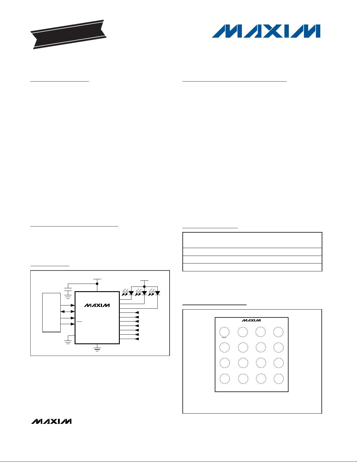
The MAX6946/MAX6947 I2C-/SMBusTM-compatible,
serial-interfaced peripherals provide microprocessors
with 10 I/O ports rated to 7V.
Each port can be configured as a 2.5mA to 20mA constant-current LED driver (static or PWM), a 1.25mA to
10mA constant-current LED driver (static or PWM), an
open-drain logic output, or an overvoltage-protected
Schmitt logic input.
Analog and switching LED intensity control includes individual 8-bit PWM control per output, individual 1-bit analog current control (half/full scale) per output, and a global
3-bit DAC current control that applies to all LED outputs.
The MAX6946/MAX6947 can stagger the PWM timing of
the 10-port outputs in consecutively phased 45° increments. Staggering the outputs spreads the PWM load
currents over time in eight steps, helping to even out
the power-supply current and reduce the RMS current.
For a similar part with an SPITM-/QSPITM-/ or MICROWIRETMcompatible interface, refer to the MAX6966/MAX6967
data sheet.
Applications
Features
♦ 2.25V to 3.6V Operation
♦ I/O Ports Default to High Impedance (LEDs Off)
on Power-Up
♦ I/O Port Inputs Are Overvoltage Protected to 7V
♦ I/O Port Outputs Are 7V-Rated Open-Drain, 10mA
or 20mA Constant-Current Static/PWM LED
Drivers, or Open-Drain Logic Outputs
♦ I/O Ports Support Hot Insertion
♦ Individual 8-Bit PWM Intensity Control for Each LED
♦ RST Input Clears Serial Interface and Can Exit
Shutdown (Warm Start)
♦ MAX6946 OSC Input Allows for External PWM
Clock Input
♦ MAX6947 AD0 Input Selects from Two Slave
Addresses
♦ Auto Ramp-Up Out of Shutdown, and Up to 4s
Hold-Off Before Ramp-Down into Shutdown
♦ 0.8µA (typ) Shutdown Current
♦ -40°C to +125°C Temperature Range
♦ Tiny WLP Package (4 x 4 Grid)
MAX6946/MAX6947
10-Port, Constant-Current LED Driver and
I/O Expander with PWM Intensity Control
________________________________________________________________ Maxim Integrated Products 1
Ordering Information
MAX6946
MAX6947
V
DD
+3.3V
μC
SDA
V
EXT
= +5V
P0
P1
P2
P3
P4
P5
P6
P7
SCL
SDA
SCL
GND
OSC*
P8
P9
LOGIC INPUT
LOGIC INPUT
LOGIC INPUT
LOGIC INPUT
LOGIC INPUT
LOGIC INPUT
LOGIC INPUT
RST
AD0**
*MAX6946 ONLY.
**MAX6947 ONLY.
Typical Operating Circuit
19-0598; Rev 3; 2/08
+Denotes a lead-free package.
*EP = Exposed pad.
Note: All devices are specified over the -40°C to +125°C operating
temperature range..
EVALUATION KIT
AVAILABLE
PART PIN-PACKAGE
PKG
CODE
MAX6946ATE+ 16 TQFN-EP* T1633-4
MAX6946CAWE+ 16 WLP W162B2-1
MAX6947ATE+ 16 TQFN-EP* T1633-4
SMBus is a trademark of Intel Corp.
SPI and QSPI are trademarks of Motorola, Inc.
MICROWIRE is a trademark of National Semiconductor Corp.
Cellular Phones
Portable Equipment
RGB LED Drivers
LCD Backlights
Keypad Backlights
LED Status Indicators
(BUMPS ON BOTTOM)
16-BUMP, 2.1mm x 2.1mm WLP
VDD
SDA
RST
SCL
OSC
P0
P9
P1
P7
P2
P8
P3
P5
P4
P6
GND
TOP VIEW
A1 A2 A3 A4
B4B3B2B1
C1 C2 C3 C4
D1 D2 D3 D4
MAX6946C
Pin Configurations
Pin Configurations continued at end of data sheet.
For pricing, delivery, and ordering information, please contact Maxim Direct at 1-888-629-4642,
or visit Maxim’s website at www.maxim-ic.com.
Page 2
MAX6946/MAX6947
10-Port, Constant-Current LED Driver and
I/O Expander with PWM Intensity Control
2 _______________________________________________________________________________________
ABSOLUTE MAXIMUM RATINGS
ELECTRICAL CHARACTERISTICS
(VDD= 2.25V to 3.6V, TA= T
MIN
to T
MAX
, unless otherwise noted. Typical values are at VDD= 3.3V, TA= +25°C.) (Note 1)
Stresses beyond those listed under “Absolute Maximum Ratings” may cause permanent damage to the device. These are stress ratings only, and functional
operation of the device at these or any other conditions beyond those indicated in the operational sections of the specifications is not implied. Exposure to
absolute maximum rating conditions for extended periods may affect device reliability.
VDD to GND .............................................................-0.3V to +4V
SCL, SDA, AD0,
RST, OSC to GND .........................-0.3V to +6V
P0 to P9 to GND .......................................................-0.3V to +8V
DC Current into P0 to P9 ....................................................24mA
DC Current into SDA ...........................................................10mA
RST Sink Current.................................................................10mA
Total GND Current ............................................................280mA
Continuous Power Dissipation (T
A
= +70°C)
16-Pin TQFN (derate 14.7mW/°C over +70°C) ..........1176mW
16-Bump WLP (derate 13.3mW/°C over +70°C)........1066mW
Operating Temperature Range (T
MIN
, T
MAX
)....-40°C to +125°C
Junction Temperature......................................................+150°C
Storage Temperature Range .............................-65°C to +150°C
Lead Temperature (soldering, 10s) .................................+300°C
PARAMETER
CONDITIONS
UNITS
Operating Supply Voltage V
DD
V
Output Load External Supply
Voltage P0–P9
V
EXT
7V
Power-On-Reset Voltage V
POR
VDD rising
V
16-pin TQFN
Power-On-Reset Voltage Hysteresis
16-bump WLP 33
mV
TA = +25°C
Standby Current Interface Idle
(PWM Disabled, All Ports High
Impedance)
I
STBY
RST at VDD;
f
SCL
= 0Hz; other digital
inputs at VDD or GND
T
A
= T
MIN
to T
MAX
µA
TA = +25°C 17 23
24
Standby Current in Reset
(PWM Disabled, All Ports High
Impedance)
I
RST
RST at GND; f
SCL
=
400kHz; other digital
inputs at VDD or GND
T
A
= T
MIN
to T
MAX
25
µA
TA = +25°C 50 60
62
Supply Current Interface Active
(Reset Run Enabled, PWM
Disabled, All Ports High
Impedance)
I
DD
f
SCL
= 400kHz; other
digital inputs at VDD or
GND
T
A
= T
MIN
to T
MAX
65
µA
TA = +25°C
One port set to 10mA
constant current; all other
ports' output registers set
to 0x00, 0x01, or 0xFF;
digital inputs at VDD or
GND
T
A
= T
MIN
to T
MAX
TA = +25°C
Delta Supply Current Interface Idle
One port set to 20mA
constant current; all other
ports' output registers set
to 0x00, 0x01, or 0xFF;
digital inputs at VDD or
GND
T
A
= T
MIN
to T
MAX
mA
SYMBOL
MIN TYP MAX
2.25 3.60
1.91
PORHYS
128
TA = T
TA = T
to +85°C 1.3
MIN
to +85°C
MIN
ΔI
DD10
TA = T
TA = T
to +85°C
MIN
to +85°C 1.9
MIN
ΔI
DD20
TA = T
to +85°C 3.8
MIN
1.0 1.3
1.5
1.58 1.8
2.0
3.2 3.6
4.0
Page 3
MAX6946/MAX6947
10-Port, Constant-Current LED Driver and
I/O Expander with PWM Intensity Control
_______________________________________________________________________________________ 3
ELECTRICAL CHARACTERISTICS (continued)
(VDD= 2.25V to 3.6V, TA= T
MIN
to T
MAX
, unless otherwise noted. Typical values are at VDD= 3.3V, TA= +25°C.) (Note 1)
PARAMETER
CONDITIONS
UNITS
Input High Voltage
(P0–P9, SDA, SCL, RST, AD0, OSC)
V
IH
P0–P9: output register set to 0x01
0.7
V
Input Low Voltage
(P0–P9, SDA, SCL, RST, AD0, OSC)
V
IL
P0–P9: output register set to 0x01
0.3
V
Input Leakage Current
(P0–P9, SDA, SCL, RST, AD0, OSC)
µA
Input Capacitance
(P0–P9, SDA, SCL, RST, AD0, OSC)
10 pF
TA = +25°C
10
16-pin TQFN
10mA Port Nominal Sink Constant
Current (P0–P9)
I
OUT
Outp ut r eg i ster set to 0x02,
V
D D
= 3.3V ,
16-bump WLP
mA
TA = +25°C
20
16-pin TQFN
20mA Port Nominal Sink Constant
Current (P0–P9)
I
OUT
Outp ut r eg i ster set to 0x02,
V
D D
= 3.3V ,
16-bump WLP
mA
TA = +25°C, VDD = 3.3V, VP0 to VP9 = 1.4V,
I
OUT
= 20mA
Port Sink Constant-Current
Matching
TA = +25°C, VDD = 3.3V, VP0 to VP9 = 1.4V,
I
OUT
= 10mA
%
Port Logic Output Low Voltage
(P0–P9)
Output register set to 0x00,
I
SINK
= 0.5mA
V
Port Logic Output Low
Short-Circuit Current (P0–P9)
Output register set to 0x00,
V
OLP_
= 5V
10
mA
Port Slew Time From 20% current to 80% current 2 µs
Output Low Voltage
(SDA)
I
SINK
= 6mA
mV
SYMBOL
IIH, I
IL
V
E X T
V
E X T
ΔI
OUT
V
OLP_
- V
- V
LE D
LE D
= 1V ( N ote 3)
= 1V ( N ote 3)
TA = T
= T
T
A
TA = T
T
= T
A
to +85°C
MIN
to +85°C
MIN
to +85°C
MIN
to +85°C
MIN
MIN TYP MAX
x V
DD
-0.2 +0.2
9.3
9.1 11.0
9.0 11.0
19.00
18.6 21.8
18.4 22.0
±2.0 ±4.0
±2.0 ±5.0
x V
DD
10.5
21.12
0.5
V
OLSDA
300
Page 4
MAX6946/MAX6947
10-Port, Constant-Current LED Driver and
I/O Expander with PWM Intensity Control
4 _______________________________________________________________________________________
TIMING CHARACTERISTICS (Figure 8)
(VDD= 2.25V to 3.6V, TA= T
MIN
to T
MAX
, unless otherwise noted. Typical values are at VDD= 3.3V, TA= +25°C.) (Note 1)
PARAMETER
CONDITIONS
UNITS
16-pin TQFN 23 32 42
Internal PWM Clock Frequency f
INT
16-bump WLP 20 32 45
kHz
External PWM Clock Frequency f
OSC
100
kHz
Serial-Clock Frequency f
SCL
400
kHz
Bus Free Time Between a STOP and
a START Condition
t
BUF
1.3 µs
Hold Time, (Repeated) START
Condition
0.6 µs
Repeated START Condition Setup
Time
0.6 µs
STOP Condition Setup Time
0.6 µs
Data Hold Time
(Note 3) 0.9 µs
Data Setup Time
180 ns
SCL Clock Low Period t
LOW
1.3 µs
SCL Clock High Period t
HIGH
0.7 µs
Rise Time of Both SDA and SCL
Signals, Receiving
t
R
(Notes 4, 5)
20
300 ns
Fall Time of Both SDA and SCL
Signals, Receiving
t
F
(Notes 4, 5)
20
300 ns
Fall Time of SDA Transmitting t
F, TX
(Notes 4, 6)
20
250 ns
Pulse Width of Spike Supressed t
SP
(Note 7) 50 ns
Capacitive Load for Each Bus Line C
b
(Note 4) 400 pF
RST Pulse Width t
W
0.1 µs
16-pin TQFN 3.0
RST Rising Edge to
MAX6946/MAX6947 ACK to Cancel
Reset Run
Reset Run enabled,
internal oscillator
enabled
16-bump WLP 2.5
ms
RST Rising Edge to
MAX6946/MAX6947 ACK to Ensure
Reset Run
Reset Run enabled, internal oscillator
enabled
5.6
ms
Note 1: All parameters are tested at TA= +25°C. Specifications over temperature are guaranteed by design.
Note 2: Port current is factory trimmed to meet a median sink current of 20mA and 10mA over all ports. The ΔI
OUT
specification
guarantees current matching between parts.
Note 3: A master device must provide a hold time of at least 300ns for the SDA signal (referred to V
IL
of the SCL signal) in order to
bridge the undefined region of SCL’s falling edge.
Note 4: Not production tested. Guaranteed by design.
Note 5: C
b
= total capacitance of one bus line in picoFarads; tRand tFare measured between 0.3 x VDDand 0.7 x VDD.
Note 6: I
SINK
≤ 6mA.
Note 7: Guaranteed by design. Input filters on the SDA and SCL inputs suppress noise spikes of less than 50ns.
SYMBOL
t
HD, STA
t
SU, STA
t
SU, STO
t
HD, DAT
t
SU, DAT
MIN TYP MAX
t
RSTRUN
t
RSTRUN
+ 0.1C
b
+ 0.1C
+ 0.1C
b
b
Page 5
MAX6946/MAX6947
10-Port, Constant-Current LED Driver and
I/O Expander with PWM Intensity Control
_______________________________________________________________________________________ 5
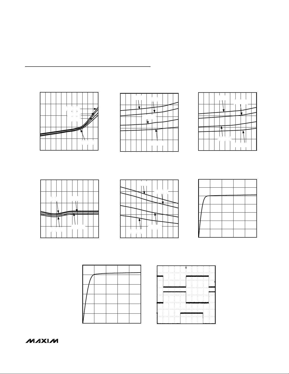
STANDBY CURRENT (I
STBY
)
vs. TEMPERATURE
TEMPERATURE (°C)
STANDBY CURRENT (μA)
MAX6946/47 toc01
-40 -25 -10 5 20 35 50 65 80 95 110 125
0
0.4
0.8
1.2
1.6
2.0
VDD = 3.6V
VDD = 3.3V
VDD = 2.7V
VDD = 2.25V
SUPPLY CURRENT (IDD)
vs. TEMPERATURE
TEMPERATURE (°C)
SUPPLY CURRENT (μA)
MAX6946/47 toc02
-40-25-105 203550658095110125
0
5
10
15
20
25
VDD = 2.25V
VDD = 2.7V
VDD = 3.3V
VDD = 3.6V
STANDBY CURRENT (I
RST
)
vs. TEMPERATURE
TEMPERATURE (°C)
STANDBY CURRENT (μA)
MAX6946/47 toc03
-40-25-10 5 203550658095110125
0
5
10
15
20
25
VDD = 2.7V
VDD = 3.6V
VDD = 3.3V
VDD = 2.25V
DELTA SUPPLY CURRENT (I
DD20
)
vs. TEMPERATURE
TEMPERATURE (°C)
DELTA SUPPLY CURRENT (mA)
MAX6946/47 toc04
-40 -25 -10 5 20 35 50 65 80 95 110 125
2.0
2.4
2.8
3.2
3.6
4.0
VDD = 3.6V
VDD = 3.3V
VDD = 2.7V
VDD = 2.25V
DELTA SUPPLY CURRENT (I
DD20
)
vs. TEMPERATURE
TEMPERATURE (°C)
DELTA SUPPLY CURRENT (mA)
MAX6946/47 toc05
-40-25-10 5 203550658095110125
0
3
6
9
12
15
VDD = 3.6V
VDD = 3.3V
VDD = 2.7V
VDD = 2.25V
OUTPUT SINKING CURRENT
vs. V
EXT
- V
LED
AT 10mA
V
EXT
- V
LED
(V)
OUTPUT SINKING CURRENT (mA)
MAX6946/47 toc06
012345
0
2
4
6
8
10
12
14
Typical Operating Characteristics
(TA = +25°C, unless otherwise noted.)
OUTPUT SINKING CURRENT
vs. V
EXT
- V
LED
AT 20mA
V
EXT
- V
LED
(V)
OUTPUT SINKING CURRENT (mA)
MAX6946/47 toc07
012345
0
4
8
12
16
20
24
STAGGER PWM PORT WAVEFORMS
(OUTPUT REGISTERS SET TO 0x80)
MAX6946/47 toc08
1ms/div
PORT P0
2V/div
PORT P4
2V/div
PORT P7
2V/div
Page 6
MAX6946/MAX6947
10-Port, Constant-Current LED Driver and
I/O Expander with PWM Intensity Control
6 _______________________________________________________________________________________
Pin Description
PIN
MAX6946/
MAX6947
MAX6946C
NAME FUNCTION
1B4 P0
2B3 P1
3C4 P2
4C3 P3
5D4 P4
I/O Ports. Configure P0–P4 as open-drain current sink outputs rated at
20mA (max), as CMOS-logic inputs, or as open-drain logic outputs.
Connect loads to a supply voltage no higher than 7V.
6 D3 GND Ground
7D2 P5
8D1 P6
9C2 P7
10 C1 P8
11 B1 P9
I/O Ports. Configure P5–P9 as open-drain current sink outputs rated at
20mA (max), as CMOS-logic inputs, or as open-drain logic outputs.
Connect loads to a supply voltage no higher than 7V.
External Oscillator Input
12 B2
Address Input. Sets the device slave address (see Table 10).
13 A1 RST Active-Low Reset Input
14 A2 VDD
P osi ti ve S up p l y V ol tag e. Byp ass V D D to GN D w i th a 0.1µF cer am i c cap aci tor .
15 A3 SCL I2C-Compatible, Serial-Clock Input
16 A4 SDA I2C-Compatible, Serial-Data I/O
—— EP
Exposed Pad on Package Underside. Connect to GND. Do not use as the
main ground connection.
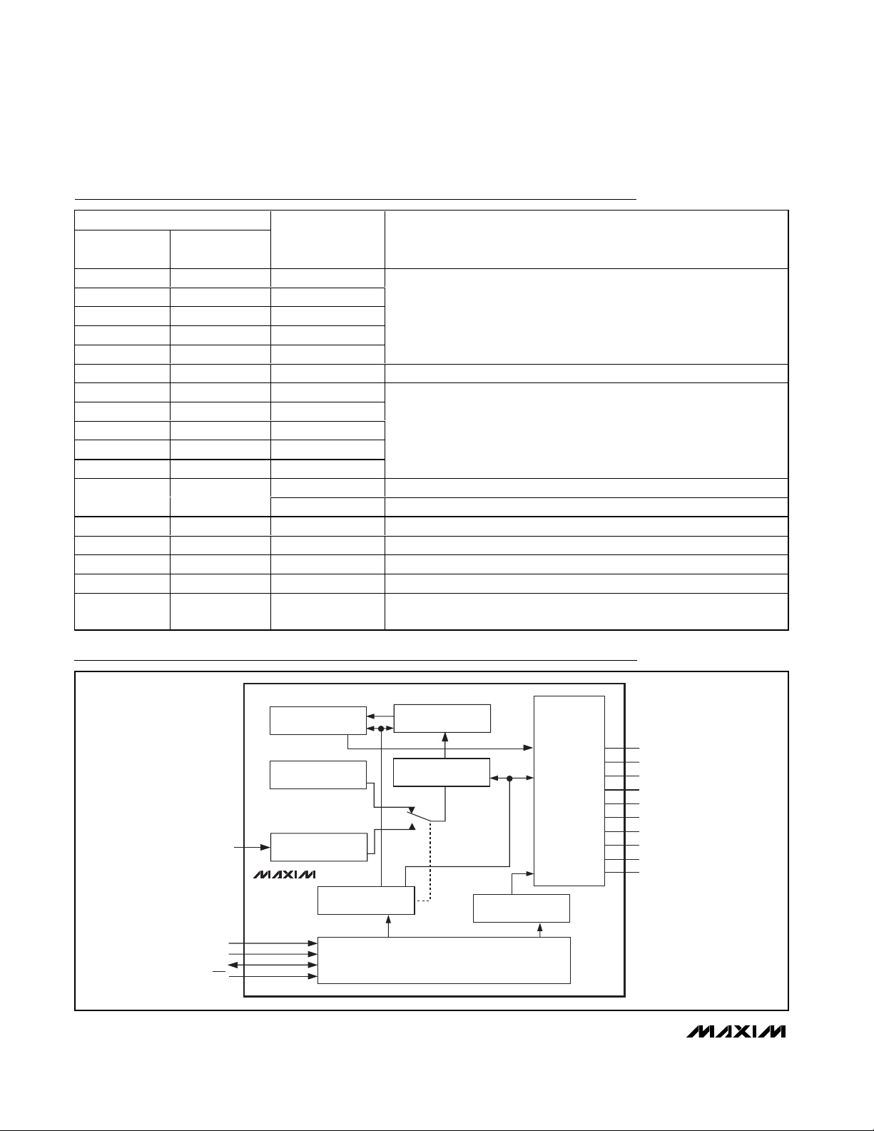
Block Diagram
OSC (MAX6946)
AD0 (MAX6947)
CURRENT REFERENCE
OSC*
EXTERNAL CLOCK INPUT*
INTERNAL
OSCILLATOR
RAMP-UP/RAMP-DOWN
PWM CONTROLLER
**MAX6946 ONLY.
**MAX6947 ONLY.
ADO**
SCL
SDA
RST
MAX6946
MAX6947
CONFIGURATION
REGISTER
2-WIRE SERIAL INTERFACE
CONTROLS
I/O REGISTER
I/O PORTS
P0
P1
P2
P3
P4
P5
P6
P7
P8
P9
Page 7
Detailed Description
The MAX6946/MAX6947 general-purpose input/output
(GPIO) peripherals provide 10 I/O ports, P0 to P9, controlled through an I2C-compatible serial interface. Use
the 10 I/O ports as logic inputs, open-drain logic outputs, or constant-current sinks in any combination.
Ports withstand 7V independent of the MAX6946/
MAX6947s’ supply voltage whether used as logic
inputs, logic outputs, or constant-current sinks.
The MAX6946/MAX6947 feature shutdown and standby
modes for low-power dissipation. The I/O ports feature
pulse-width modulation (PWM) of the outputs and can
stagger the PWM timing of the 10 port outputs in consecutively phased 45° increments. The I/O ports also
feature ramp-up and ramp-down controls.
The MAX6946/MAX6947 feature a RST input to halt any
serial-interface transmission and bring the device out of
shutdown.
Open-drain logic outputs require external pullup resistors to provide the logic-high reference. Ports configured as open-drain logic outputs have a relatively weak
sink capability, but are still adequate for normal logiclevel outputs. The weak drive means that the short-circuit current is low enough that inadvertently driving an
LED from a port configured as a logic output is unlikely
to damage the LED.
The MAX6946 features a fixed I2C slave address of
010 0000 and provides an OSC input to accept an
external PWM clock input as an alternative to the internal PWM clock.
The MAX6947 features an AD0 input that uses two-level
logic to select from two I2C slave addresses. The
MAX6947 always uses the internal PWM clock.
Register Structure
The MAX6946/MAX6947 contain 22 internal registers
(see Table 1). Use registers 0x00 to 0x09 to individually
control ports P0 to P9. Registers 0x0A to 0x0D allow
more than one port control register to be written with
the same data to simplify software. Registers 0x0E and
0x0F do not store data, but return the port input status
when read. Registers 0x10 to 0x15 configure and control the device operation.
MAX6946/MAX6947
10-Port, Constant-Current LED Driver and
I/O Expander with PWM Intensity Control
_______________________________________________________________________________________ 7
Table 1. Register Address Map
DESCRIPTION
ADDRESS
CODE
(HEX)
AUTO-
INCREMENT
ADDRESS
Port P0 output level or PWM 0x00 0x01
Port P1 output level or PWM 0x01 0x02
Port P2 output level or PWM 0x02 0x03
Port P3 output level or PWM 0x03 0x04
Port P4 output level or PWM 0x04 0x05
Port P5 output level or PWM 0x05 0x06
Port P6 output level or PWM 0x06 0x07
Port P7 output level or PWM 0x07 0x08
Port P8 output level or PWM 0x08 0x09
Port P9 output level or PWM 0x09 0x10
Write ports P0–P9 with same
output level or PWM
Read port P0 output level or PWM
0x0A 0x10
Write ports P0–P3 with same
output level or PWM
Read port P0 output level or PWM
0x0B 0x10
Write ports P4–P7 with same
output level or PWM
Read port P4 output level or PWM
0x0C 0x10
Write ports P8 or P9 with same
output level or PWM
Read port P8 output level or PWM
0x0D 0x10
Read ports P7–P0 inputs 0x0E 0x0F
Read p or ts P 9 and P 8 i np uts 0x0F 0x0E
Configuration 0x10 0x11
Ramp-down 0x11 0x12
Ramp-up 0x12 0x13
Output current ISET70 0x13 0x14
Output current ISET98 0x14 0x15
Global current 0x15 0x10
Factory reserved; do not write to
this register
0x7D —
Page 8
MAX6946/MAX6947
Configuration Register (0x10)
Use the configuration register to select PWM phasing
between outputs, test fade status, enable hardware
startup from shutdown, and select shutdown or run
mode (Table 2).
Initial Power-Up
All control registers reset upon power-up (Table 3).
Power-up status sets I/O ports P0 to P9 to high impedance, and puts the device into shutdown. The
MAX6946/MAX6947 powers up in shutdown.
10-Port, Constant-Current LED Driver and
I/O Expander with PWM Intensity Control
8 _______________________________________________________________________________________
Table 2. Configuration Register (0x10)
REGISTER BIT DESCRIPTION
VALUE
FUNCTION
0 Internal oscillator enabled as PWM clock source
D7 OSC enable*
1 External oscillator input enabled as PWM clock source
0 RST does not change register data
D6 RSTPOR options
1 RST resets registers to POR (power-on reset) state
0 PWM outputs are in phase
D5 PWM stagger
1 PWM outputs stagger phase
0 Device not in hold-off
D4 Hold-off status**
1 Device in hold-off
0 Device not in fade-off
D3 Fade-off status**
1 Device in fade-off
0 Device not in ramp-up
D2 Ramp-up status**
1 Device in ramp-up
0 Reset Run disabled
D1 RST RUN enable
1 Reset Run enabled
0 Shutdown mode
D0 RUN enable
1 Run mode
*The OSCEN bit applies only to the MAX6946. OSCEN is always 0 for the MAX6947, and the MAX6947 ignores writes to the OSCEN bit.
**Read-only bits.
Table 3. Initial Power-Up Register Status
REGISTER BIT
DESCRIPTION POWER-UP CONDITION
ADDRESS
D0
Port P0–P9 output level
or PWM
Port 0–9 high impedance
1
1
Configuration
0x10
0
0
Ramp-down/hold-off Fade/hold-off disabled 0x11
0
0
Ramp-up Disabled 0x12
0
0
I
PEAK
= 10mA for ports P7–P0 0x13
0
0
I
PEAK
= 10mA for ports P9, P8 0x14
0
0
Global current Full current 0x15
1
1
*Value is 0 for MAX6947 and 1 for MAX6946 bit.
S hutd ow n m od e, Reset Run d i sa b l ed
Output current ISET70
Output current ISET98
CODE (HEX)
0x00–0x09 11111
D7 D6 D5 D4 D3 D2 D1
0/1* 0000
00000
00000
00000
00000
00000
1
0
0
0
0
0
1
Page 9

I/O Ports
The MAX6946/MAX6947 contain 10 I/O ports.
Configure the 10 I/O ports as logic inputs, open-drain
logic outputs, or constant-current sinks in any combination. Table 4 shows a detailed description of the individual port configuration registers 0x00 through 0x09.
Use registers 0x00–0x09 to individually assign each
port as a logic input, open-drain logic output or constant-current sink (see the PWM Intensity Control and
Phasing section). The I/O ports are high impedance
without VDDapplied and remain high impedance upon
power-up.
Figure 1 shows the I/O port structure of the MAX6946/
MAX6947. I/O ports P0 to P9 default to high impedance
on power-up, so LEDs or other port loads connected
draw no current. Ports used as inputs do not load their
source signals.
MAX6946/MAX6947
10-Port, Constant-Current LED Driver and
I/O Expander with PWM Intensity Control
_______________________________________________________________________________________ 9
Figure 1. Simplified Schematic of I/O Ports
Table 4. Individual Port Configuration Options (Port Output Registers 0x00–0x09)
PORT TYPE
OUTPUT
REGISTER
CODE
RUN MODE (CONFIGURATION
REGISTER BIT D0 = 1)
SHUTDOWN
(CONFIGURATION REGISTER
BIT D0 = 0)
APPLICATION NOTES
Low-logic
output
0x00 Logic-low output, not constant current
High-logic
output
Logic-high output with external pullup resistor;
otherwise, high impedance
Logic input
0x01
CMOS logic input
Lowest supply current,
unaffected by shutdown
Constantcurrent static
sink output
0x02
Static constant-current sink
output
Full constant-current drive
with no PWM
Constantcurrent PWM
output
0x03 = 3/256 PWM duty cycle
High impedance
Adjustable constant current
LED off 0xFF
Logic-high output with external pullup resistor; otherwise,
high impedance
LED off
POSITION A: 0x00–0x01
POSITION B: 0x02–0xFF
CLOSE SWITCH: 0x02–0xFE
8-BIT LATCH
OUTPUT PORT
REGISTER
TO/FROM
SERIAL
INTERFACE
1-BIT LATCH
OUTPUT CURRENT
REGISTER
3-BIT LATCH
GLOBAL CURRENT
REGISTER
PORT COMMAND
MSB
READ I/O
I/O PORT
AB
PWM
GENERATOR
4-BIT DAC
ENABLE
SET
CURRENT
ENABLE = 0x00
N
0x03–0xFE
0xFE = 254/256 PWM duty cycle
Page 10

MAX6946/MAX6947
Ports Configured as Outputs
The global-current register sets the full (maximum) constant-current sink into an I/O port configured as an output (Table 5). Each output port’s individual constantcurrent sink can set to either half or full scale of the
global current by the output-current registers (Table 6).
By default, maximum current is 20mA, hence the default
maximum half current is 10mA.
Set each output port’s individual constant-current sink
to either half scale or full scale of the global current.
Use the output-current registers to set the individual
currents (Table 6). Set the global current by the globalcurrent register (Table 5).
Set each output current individually to best suit the
maximum operating current of an LED load, or even
adjust on the fly to double the effective intensity control
range of each output. The individual current selection is
10mA (half) or 20mA (full) when setting the global-current register to its maximum value.
10-Port, Constant-Current LED Driver and
I/O Expander with PWM Intensity Control
10 ______________________________________________________________________________________
Table 5. Global-Current Register Format (0x15)
REGISTER BIT
DESCRIPTION
D7 D6 D5 D4 D3 D2 D1 D0
Full current is 2.5mA; half current is 1.25mA X X X X X 0 0 0
Full current is 5mA; half current is 2.5mA X X X X X 0 0 1
Full current is 7.5mA; half current is 3.75mA X X X X X 0 1 0
Full current is 10mA; half current is 5mA X X X X X 0 1 1
Full current is 12.5mA; half current is 6.25mA X X X X X 1 0 0
Full current is 15mA; half current is 7.5mA X X X X X 1 0 1
Full current is 17.5mA; half current is 8.75mA X X X X X 1 1 0
Full current is 20mA; half current is 10mA X X X X X 1 1 1
Table 6. Output-Current Register Format
REGISTER BIT
DESCRIPTION
ADDRESS
D7 D6 D5 D4 D3 D2 D1 D0
Output P0 is set to half constant current X X X X X X X 0
Output P0 is set to full constant current X X X X X X X 1
Output P1 is set to half constant current X X X X X X 0 X
Output P1 is set to full constant current X X X X X X 1 X
Output P2 is set to half constant current X X X X X 0 X X
Output P2 is set to full constant current X X X X X 1 X X
Output P3 is set to half constant current X X X X 0 X X X
Output P3 is set to full constant current X X X X 1 X X X
Output P4 is set to half constant current X X X 0 X X X X
Output P4 is set to full constant current X X X 1 X X X X
Output P5 is set to half constant current X X 0 X X X X X
Output P5 is set to full constant current X X 1 X X X X X
Output P6 is set to half constant current X 0 X X X X X X
Output P6 is set to full constant current X 1 X X X X X X
Output P7 is set to half constant current 0 X X X X X X X
Output P7 is set to full constant current
0x13
1XXXXX XX
Output P8 is set to half constant current X X X X X X X 0
Output P8 is set to full constant current X X X X X X X 1
Output P9 is set to half constant current X X X X X X 0 X
Output P9 is set to full constant current
0x14
XXXXXX1X
CODE (HEX)
Page 11

MAX6946/MAX6947
10-Port, Constant-Current LED Driver and
I/O Expander with PWM Intensity Control
______________________________________________________________________________________ 11
PWM Intensity Control and Phasing
The MAX6946/MAX6947 use an internal 32kHz oscillator to generate PWM timing for LED intensity control.
The MAX6946 also features an OSC input to allow for
an external clock for generating PWM timing for LED
intensity control. Select the PWM clock source for the
MAX6946 with configuration register bit D7 (Table 2).
The MAX6947 powers up configured to use the internal
32kHz oscillator by default. The MAX6946 powers up
configured to use the external clock source by default.
A PWM period comprises 256 cycles of the nominal
32kHz PWM clock (Figure 2). Individually set the ports’
PWM duty cycle between 3/256 and 254/256. See
Table 4 for port register settings.
Configure PWM timing by setting the stagger bit in the
configuration register (Table 2), either with output staggering or without. Clearing the stagger bit causes all
outputs using PWM to switch at the same time using
the timing shown in Figure 2. All outputs, therefore,
draw load current at the exactly same time for the same
PWM setting. This means that if, for example, all outputs are set to 0x80 (128/256 duty cycle), the current
draw would be zero (all loads off) for half the time, and
full (all loads on) for the other half.
Setting the stagger bit causes the PWM timing of the 10
port outputs to stagger by 32 counts of the 256-count
PWM period (i.e., 1/8th), distributing the port output
switching points across the PWM period (Figure 3).
Staggering reduces the di/dt output-switching transient
on the supply and also reduces the peak/mean current
requirement.
Set or clear the stagger bit during shutdown. Changing
the stagger bit during normal operation can cause a
transient flicker in any PWM-controlled LEDs because
of the fundamental PWM timing changes.
HIGH-Z
LOW
HIGH-Z
LOW
HIGH-Z
LOW
OUTPUT LOW 254/256 DUTY CONSTANT CURRENT WITH INPUT BUFFER DISABLED (PWM LED DRIVE)
HIGH-Z
LOW
0xFF
HIGH-Z
LOW
HIGH-Z
LOW
OUTPUT LOW 253/256 DUTY CONSTANT CURRENT WITH INPUT BUFFER DISABLED (PWM LED DRIVE)
OUTPUT STATIC-HIGH LOGIC DRIVE WITH INPUT BUFFER ENABLED (GPI)
OUTPUT STATIC-LOW LOGIC DRIVE WITH INPUT BUFFER ENABLED (GPI)
OUTPUT STATIC-LOW CONSTANT CURRENT WITH INPUT BUFFER DISABLED (STATIC LED DRIVE ON)
0xFD
0xFE
0x02
0x00
0x01
OUTPUT STATIC HIGH IMPEDANCE WITH INPUT BUFFER DISABLED (STATIC LED DRIVE OFF)
HIGH-Z
LOW
OUTPUT LOW 3/256 DUTY CONSTANT CURRENT WITH INPUT BUFFER DISABLED (PWM LED DRIVE)
0x03
HIGH-Z
LOW
OUTPUT LOW 252/256 DUTY CONSTANT CURRENT WITH INPUT BUFFER DISABLED (PWM LED DRIVE)
0xFC
REGISTER
VALUE
OUTPUT
7.8125ms NOMINAL PWM PERIOD
HIGH-Z
LOW
OUTPUT LOW 4/256 DUTY CONSTANT CURRENT WITH INPUT BUFFER DISABLED (PWM LED DRIVE)
0x04
Figure 2. Static and PWM Constant-Current Waveforms
Page 12

MAX6946/MAX6947
Ports Configured as Inputs
Configure a port as a logic input by writing 0x01 to the
port’s output register (Table 4). Reading an input port
register returns the logic levels from the I/O ports configured as a logic input (Table 7). The input port register returns logic 0 in the appropriate bit position for a
port not configured as a logic input.
The input port’s registers are read only. The MAX6946/
MAX6947 ignore a write to input ports register.
RST
Input
The active-low RST input operates as a reset that voids
any current I2C transaction involving the MAX6946/
MAX6947, forcing the devices into the I2C stop condition. Use the D6 bit in the configuration register to configure RST to reset all the internal registers to the
power-on reset state (Tables 2 and 3). The RST input is
overvoltage tolerant to 6V.
The MAX6946/MAX6947 ignore all I2C bus activity while
RST remains low. The MAX6946/MAX6947 use this feature to minimize supply current in power-critical applications by effectively disconnecting the MAX6946/
MAX6947 from the bus during idle periods. RST also
operates as a bus multiplexer, allowing multiple
MAX6946/MAX6947s to use the same I2C slave address.
Drive only one MAX6946/MAX6947 RST input high at any
time to use RST as a bus multiplexer.
The MAX6946/MAX6947 feature a Reset Run option so
that simply taking the RST input high brings the driver
out of shutdown in addition to its normal function of
enabling the devices’ I2C interface.
Standby Mode and Operating Current
Configuring all the ports as logic inputs or outputs (all
output registers set to value 0x00 or 0x01) or LED off
(output register set to value 0xFF) puts the MAX6946/
MAX6947 into standby mode. Put the MAX6946/
MAX6947 into standby mode for lowest supply-current
consumption.
Setting a port as a constant-current output increases
the operating current (output register set to a value
between 0x02 and 0xFE), even if a load is not applied
to the port. The MAX6946/MAX6947 enable an internal
current mirror to provide the accurate constant-current
sink. Enabling the internal current mirror increases the
devices’ supply current. Each output contains a gated
mirror, and each mirror is only enabled when required.
In PWM mode, the current mirror is only turned on for
the output’s on-time. This means that the operating current varies as constant-current outputs are turned on
and off through the serial interface, as well as by the
PWM intensity control.
10-Port, Constant-Current LED Driver and
I/O Expander with PWM Intensity Control
12 ______________________________________________________________________________________
7.8125ms NOMINAL PWM PERIOD NEXT PWM PERIOD NEXT PWM PERIOD
0 32 64 96 128 160 192 224 256
OUTPUTS P0, O8 IN-PHASE PWM PERIOD
OUTPUT P1, O9 STAGGERED PWM PERIOD
OUTPUT P3 STAGGERED PWM PERIOD
OUTPUT P4 STAGGERED PWM PERIOD
OUTPUT P5 STAGGERED PWM PERIOD
OUTPUT P6 STAGGERED PWM PERIOD
OUTPUT P7 STAGGERED PWM PERIOD
OUTPUTS P0, O8 IN-PHASE PWM PERIOD
OUTPUT P1, O9 STAGGERED PWM PERIOD
OUTPUT P3 STAGGERED PWM PERIOD
OUTPUT P4 STAGGERED PWM PERIOD
OUTPUT P5 STAGGERED PWM PERIOD
OUTPUT P6 STAGGERED PWM PERIOD
OUTPUT P7 STAGGERED PWM PERIOD
OUTPUTS P0, O8 IN-PHASE PWM PERIOD
OUTPUT P1, O9 STAGGERED PWM PERIOD
OUTPUT P2 STAGGERED PWM PERIOD OUTPUT P2 STAGGERED PWM PERIOD
Figure 3. Staggered PWM Waveform
Table 7. Input Ports Registers
REGISTER BIT
DESCRIPTION
ADDRESS
D7 D6 D5 D4 D3 D2 D1 D0
Input ports
P7–P0
0x0E
Port P0
Input ports
P9 and P8
0x0F 0 0 0 0 0 0
Port P8
CODE (HEX)
Port P7 Port P6 Port P5 Port P4 Port P3 Port P2 Port P1
Port P9
Page 13

Shutdown Mode
In shutdown mode, all ports configured as constantcurrent outputs (output register set to a value between
0x02 and 0xFE) are switched off, and these outputs go
high impedance as if their registers were set to value
0xFF. Ports configured as logic inputs or outputs (output registers set to value 0x00 or 0x01) are unaffected
(Table 4). This means that any ports used for GPIOs
are still fully operational in shutdown mode, and port
inputs can be read and output ports can be toggled at
any time using the serial interface. Use the MAX6946/
MAX6947 for a mix of logic inputs, logic outputs, and
PWM LED drivers, and only the LED drivers turn off
automatically in shutdown.
Put the MAX6946/MAX6947 into shutdown mode by
clearing the run bit (bit D0) in the configuration register
(0x10) (Table 2). Exit shutdown by setting the run bit high
through the serial interface or by using the Reset Run
option (see the Reset Run Option section). Configure
and control the MAX6946/MAX6947 normally through the
serial interface in shutdown mode. All registers are
accessible in shutdown mode, and shutdown mode
does not change any register values.
Changing a port from static logic-low (0x00) or static
logic-high (0x01) to a constant-current value
(0x02–0xFE) in shutdown mode turns that output off
(logic-high or high impedance) like any other constantcurrent outputs in shutdown. The new constant-current
output starts just like any other constant-current outputs
when exiting shutdown.
Changing a port from a constant-current value
(0x02–0xFE) to static logic-low (0x00) or static logichigh (0x01) in shutdown causes that output to set to the
value as a GPIO output. The new GPIO output is unaffected just like any other GPIO output when exiting
shutdown.
Ramp-Up and Ramp-Down Controls
The MAX6946/MAX6947 provide controls that allow the
output currents to ramp down into shutdown (rampdown), and ramp up again out of shutdown (ramp-up)
(Figures 4 and 5). Ramp-down comprises a programmable hold-off delay that also maintains the outputs at full
current for a time before the programmed fade-off time.
After the hold-off delay, the output currents ramp down.
MAX6946/MAX6947
10-Port, Constant-Current LED Driver and
I/O Expander with PWM Intensity Control
______________________________________________________________________________________ 13
EXIT SHUTDOWN COMMAND
FULL CURRENT/
HALF CURRENT
0
1s 2s1/4s 1/2s
1/8s
1/16s
ZERO TO 4s CURRENT RAMP-UP AFTER CS RUN
4s
Figure 4. Ramp-Up Behavior
ZERO TO 4s HOLD-OFF DELAY BEFORE FADE-OFF
ZERO TO 4s CURRENT FADE-OFF AFTER HOLD-OFF DELAY
1s 2s 4s 1s 2s
1/8s
1/16s
1/8s
1/16s
ZERO TO 8s CURRENT RAMP-DOWN
4s1/4s 1/2s 1/4s 1/2s
FULL CURRENT/
HALF CURRENT
0
Figure 5. Ramp-Down, Hold-Off, and Fade-Off Behavior
Page 14

MAX6946/MAX6947
The ramp-down register sets the hold-off and fade-off
times and allows disabling of hold-off and fade-off (zero
delay), if desired (Table 8). The ramp-up register sets
the ramp-up time and allows disabling of ramp-up (zero
delay), if desired (Table 9). The configuration register
contains three status bits that identify the condition of
the MAX6946/MAX6947, hold-off, fade-off, or ramp-up
(Table 2). The configuration register also enables or disables ramp-up. One write command to the configuration
register can put the MAX6946/MAX6947 into shutdown
(using hold-off and fade-off settings in the fade register)
and one read command to the configuration register can
determine whether the Reset Run is enabled for restart,
and whether the MAX6946/MAX6947 will use ramp-up
on restart.
10-Port, Constant-Current LED Driver and
I/O Expander with PWM Intensity Control
14 ______________________________________________________________________________________
20mA
15mA
10mA
5mA
0mA
CURRENT
FADE-UP
FULL
CURRENT
7/8
CURRENT
6/8
CURRENT
5/8
CURRENT
4/8
CURRENT
3/8
CURRENT
2/8
CURRENT
1/8
CURRENT
ZERO
CURRENT
17.5mA
12.5mA
7.5mA
2.5mA
PORT CURRENT = HALF
FADE-OFF
PORT CURRENT = FULL
Figure 6. Output Fade DAC (Global Current = 0x07)
Table 8. Ramp-Down Register Format (0X11)
REGISTER BIT
DESCRIPTION
D0
Instant going into shutdown after hold-off delay X X X X X 0 0 0
1/16s ramp-down from full current before shutdown after hold-off delay X X X X X 0 0 1
1/8s ramp-down from full current before shutdown after hold-off delay X X X X X 0 1 0
1/4s ramp-down from full current before shutdown after hold-off delay X X X X X 0 1 1
1/2s ramp-down from full current before shutdown after hold-off delay X X X X X 1 0 0
1s ramp-down from full current before shutdown after hold-off delay X X X X X 1 0 1
2s ramp-down from full current before shutdown after hold-off delay X X X X X 1 1 0
4s ramp-down from full current before shutdown after hold-off delay X X X X X 1 1 1
Zero hold-off delay before fade-off going into shutdown X X 0 0 0 X X X
1/16s hold-off delay before fade-off going into shutdown X X 0 0 1 X X X
1/8s hold-off delay before fade-off going into shutdown X X 0 1 0 X X X
1/4s hold-off delay before fade-off going into shutdown X X 0 1 1 X X X
1/2s hold-off delay before fade-off going into shutdown X X 1 0 0 X X X
1s hold-off delay before fade-off going into shutdown X X 1 0 1 X X X
2s hold-off delay before fade-off going into shutdown X X 1 1 0 X X X
4s hold-off delay before fade-off going into shutdown X X 1 1 1 X X X
D7 D6 D5 D4 D3 D2 D1
Page 15

Ramp-up and ramp-down use the PWM clock for timing. When using the external oscillator make sure the
oscillator runs until the end of the sequence. The internal oscillator always runs during a fade sequence, even
if none of the ports use PWM.
The ramp-up and ramp-down circuit operates a 3-bit
DAC. The DAC adjusts the internal current reference
used to set the constant-current outputs in a similar
manner to the global-current register (Table 5). The
MAX6946/MAX6947 scale the master current reference
so all output constant-current and PWM settings adjust
at the same ratio with respect to each other. This
means the LEDs always fade at the same rate even if
with different intensity settings.
The maximum port output current set by the global-current register (Table 5) also sets the point during rampdown that the current starts falling, and the point during
ramp-up that the current stops rising. Figure 7 shows
the ramp waveforms that occur with different globalcurrent register settings.
Reset Run Option
The MAX6946/MAX6947 feature a Reset Run option so
that simply taking the RST input high brings the driver
out of shutdown in addition to its normal function of
enabling the MAX6946/MAX6947s’ I2C interface. This
provides an alternative method of bringing the driver
out of shutdown to writing to the configuration register
through the serial interface. The Reset Run timing uses
the PWM clock, either the internal nominal 32kHz oscillator or a user-provided clock fed into the OSC input
(MAX6946 only).
After enabling the Reset Run option, the MAX6946/
MAX6947 use the rising edge on RST, followed by no
I2C interface activity to the MAX6946/MAX6947 for 128
to 129 periods of the PWM clock to trigger the Reset
Run option. If this timeout period elapses without the
MAX6946/MAX6947 acknowledging an I2C transaction,
the run bit (D0) in the configuration register sets, bringing the driver out of shutdown and activating any programmed ramp-up. If RST pulses high for less than this
timeout period to trigger a Reset Run, the MAX6946/
MAX6947 ignore the pulse, and the MAX6946/MAX6947
continue to wait for a suitable trigger.
Cancel the Reset Run trigger by transmitting an I2C
communication to the MAX6946/MAX6947 before the
timeout period elapses. The trigger cancels when the
MAX6946/MAX6947 acknowledge the I2C transaction
MAX6946/MAX6947
10-Port, Constant-Current LED Driver and
I/O Expander with PWM Intensity Control
______________________________________________________________________________________ 15
20mA
15mA
10mA
5mA
0mA
CURRENT
FULL
CURRENT
7/8
CURRENT
6/8
CURRENT
5/8
CURRENT
4/8
CURRENT
3/8
CURRENT
2/8
CURRENT
1/8
CURRENT
ZERO
CURRENT
17.5mA
12.5mA
7.5mA
2.5mA
RAMP-UP
RAMP-DOWN
GLOBAL CURRENT = 0x07
GLOBAL CURRENT = 0x06
GLOBAL CURRENT = 0x05
GLOBAL CURRENT = 0x04
GLOBAL CURRENT = 0x03
GLOBAL CURRENT = 0x02
GLOBAL CURRENT = 0x01
GLOBAL CURRENT = 0x00
Figure 7. Global Current Modifies Fade Behavior
Table 9. Ramp-Up Register Format (0x12)
REGISTER BIT
DESCRIPTION
D7 D6 D5 D4 D3 D2 D1 D0
Instant full current coming out from shutdown X X X X X 0 0 0
1/16s ramp-up to full current coming out from shutdown X X X X X 0 0 1
1/8s ramp-up to full current coming out from shutdown X X X X X 0 1 0
1/4s ramp-up to full current coming out from shutdown X X X X X 0 1 1
1/2s ramp-up to full current coming out from shutdown X X X X X 1 0 0
1s ramp-up to full current coming out from shutdown X X X X X 1 0 1
2s ramp-up to full current coming out from shutdown X X X X X 1 1 0
4s ramp-up to full current coming out from shutdown X X X X X 1 1 1
Page 16

MAX6946/MAX6947
and requires sending at least the MAX6946/MAX6947s’
I2C slave address. When using the internal oscillator,
the minimum timeout period is 127/45000 equal to
2.822ms. When using an external oscillator for the PWM
clock, the timeout period is 127/OSC. The shortest time
period allowed is 1.27ms; this number corresponds to
the maximum OSC frequency of 100kHz. When using
the internal oscillator, the minimum I2C clock speed
that guarantees a successful start bit and eight data
bits (9 bits total) within the minimum timeout period is
9/5.66ms equal to 1590Hz. Canceling the Reset Run
trigger clears the Reset Run bit (D1) in the configuration register, disabling Reset Run. The run bit (D0) in
the configuration register remains cleared, so the driver
remains in shutdown.
OSC Input
The MAX6946 can use an external clock of up to
100kHz instead of the internal 32kHz oscillator.
Connect the external clock to the OSC input and set the
OSC bit in the configuration register to enable the
MAX6946 to use the external clock (Table 2).
Serial Interface
Serial Addressing
The MAX6946/MAX6947 operate as a slave that sends
and receives data through an I
2
C-compatible, 2-wire
interface. The interface uses a serial-data line (SDA)
and a serial-clock line (SCL) to achieve bidirectional
communication between master(s) and slave(s). A
master (typically a microcontroller) initiates all data
transfers to and from the MAX6946/MAX6947 and generates the SCL clock that synchronizes the data transfer (Figure 8).
The MAX6946/MAX6947 SDA line operates as both an
input and an open-drain output. A pullup resistor, typically 4.7kΩ, is required on SDA. The MAX6946/
MAX6947 SCL line operates as an input. A pullup resistor, typically 4.7kΩ, is required on SCL if there are multiple masters on the 2-wire interface, or if the master in
a single-master system has an open-drain SCL output.
Each transmission consists of a START condition
(Figure 9) sent by a master, followed by the MAX6946/
MAX6947 7-bit slave address plus the R/W bit, a register address byte, one or more data bytes, and finally a
STOP condition (Figure 9).
10-Port, Constant-Current LED Driver and
I/O Expander with PWM Intensity Control
16 ______________________________________________________________________________________
SCL
SDA
t
R
t
F
t
BUF
START
CONDITION
STOP
CONDITION
REPEATED START CONDITION
START CONDITION
t
SU,STO
t
HD,STA
t
SU,STA
t
HD,DAT
t
SU,DAT
t
LOW
t
HIGH
t
HD,STA
Figure 8. 2-Wire Serial Interface Timing Details
Page 17

Start and Stop Conditions
Both SCL and SDA remain high when the interface is
not busy. A master signals the beginning of a transmission with a START (S) condition by transitioning SDA
from high to low while SCL is high. When the master finishes communicating with the slave, it issues a STOP
(P) condition by transitioning SDA from low to high
while SCL is high. The bus is then free for another
transmission (Figure 9).
Bit Transfer
One data bit is transferred during each clock pulse.
The data on SDA must remain stable while SCL is high
(Figure 10).
Acknowledge
Any bytes received after the command byte are data
bytes. The first data byte goes into the internal register
of the MAX6946/MAX6947 selected by the command
byte (Figure 11). If multiple data bytes are transmitted
before a STOP condition is detected, these bytes are
generally stored in subsequent MAX6946/MAX6947
internal registers because the command byte autoincrements (Table 1).
Message Format for Reading
Read from the MAX6946/MAX6947 using the
MAX6946/MAX6947s’ internally stored command byte
as an address pointer the same way the stored command byte is used as an address pointer for a write.
The pointer autoincrements after each data byte is read
using the same rules as for a write (Table 1). Thus, a
read is initiated by first configuring the MAX6946/
MAX6947s’ command byte by performing a write
(Figures 12 and 13). The master can now read n con-
secutive bytes from the MAX6946/MAX6947 with the
first data byte being read from the register addressed
by the initialized command byte (Figure 14). When performing read-after-write verification, remember to reset
the command byte’s address because the stored command byte address has been autoincremented after
the write (Table 1).
MAX6946/MAX6947
10-Port, Constant-Current LED Driver and
I/O Expander with PWM Intensity Control
______________________________________________________________________________________ 17
Table 10. MAX6946/MAX6947 Slave
Addresses
MAX6947 SLAVE ADDRESS
AD0 = GND 010 0000
AD0 = V
DD
010 0100
MAX6946 010 0000
Figure 9. Start and Stop Conditions
SDA
SCL
DATA LINE STABLE;
DATA VALID
CHANGE OF DATA
ALLOWED
Figure 10. Bit Transfer
SCL
SDA BY
TRANSMITTER
CLOCK PULSE
FOR ACKNOWLEDGE
START
CONDITION
SDA BY
RECEIVER
12 89
S
Figure 11. Acknowledge
SDA
SCL
SP
START
CONDITION
STOP
CONDITION
Page 18

MAX6946/MAX6947
Operation with Multiple Masters
If the MAX6946/MAX6947 operates on a 2-wire interface with multiple masters, a master reading the
MAX6946/MAX6947 should use a repeated start
between the write. This sets the MAX6946/MAX6947
address pointer, and the read(s) that takes the data
from the location(s) (Table 1). This is because it is possible for master 2 to take over the bus after master 1
has set up the MAX6946/MAX6947s’ address pointer,
then master 1’s delayed read can be from an unexpected location.
Command Address Autoincrementing
The command address stored in the MAX6946/
MAX6947 increments through the grouped register functions after each data byte is written or read (Table 1).
Applications Information
Port Input and I2C Interface-Level
Translation from Higher or
Lower Logic Voltages
The MAX6946/MAX6947s’ I2C interface (SDA, SCL) and
I2C slave address select input AD0 (MAX6947 only),
PWM clock input OSC (MAX6946 only), and reset input
RST are overvoltage protected to +6V, independent of
VDD. The 10 I/O ports P0–P9 are overvoltage protected
to +8V independent of VDD. This allows the MAX6946/
MAX6947 to operate from one supply voltage, such as
3.3V, while driving the I2C interface and/or some of the
10 I/O as inputs from a higher logic level, such as 5V.
10-Port, Constant-Current LED Driver and
I/O Expander with PWM Intensity Control
18 ______________________________________________________________________________________
SAA
P
0SLAVE ADDRESS COMMAND BYTE
ACKNOWLEDGE FROM MAX6946/MAX6947
D15 D14 D13 D12 D11 D10 D9 D8
COMMAND BYTE IS STORED ON RECEIPT OF
STOP CONDITION
ACKNOWLEDGE FROM MAX6946/MAX6947
R/W
Figure 12. Command Byte Received
SAAAP0SLAVE ADDRESS COMMAND BYTE DATA BYTE
1
BYTE
AUTOINCREMENT MEMORY ADDRESS
D15 D14 D13 D12 D11 D10 D9 D8 D1 D0D3 D2D5 D4D7 D6
ACKNOWLEDGE FROM MAX6946/MAX6947 ACKNOWLEDGE FROM MAX6946/MAX6947
ACKNOWLEDGE FROM MAX6946/MAX6947
HOW COMMAND BYTE AND DATA BYTE MAP INTO
MAX6946/MAX6947s' REGISTERS
R/W
Figure 13. Command and Single Data Byte Received
SAAAP0SLAVE ADDRESS COMMAND BYTE DATA BYTE
N
BYTES
D15 D14 D13 D12 D11 D10 D9 D8 D1 D0D3 D2D5 D4D7 D6
ACKNOWLEDGE FROM MAX6946/MAX6947 ACKNOWLEDGE FROM MAX6946/MAX6947
ACKNOWLEDGE FROM MAX6946/MAX6947
HOW COMMAND BYTE AND DATA BYTE MAP INTO
MAX6946/MAX6947s' REGISTERS
R/W
AUTOINCREMENT MEMORY ADDRESS
Figure 14. n Data Bytes Received
Page 19

Hot Insertion
The RST, SCL, and AD0 inputs and SDA remain high
impedance with up to +6V asserted on them when the
MAX6946/MAX6947 power down (VDD= 0V). I/O ports
P0 to P9 remain high impedance with up to +8V asserted
on them when the MAX6946/MAX6947 power down. Use
the MAX6946/MAX6947 in hot-swap applications.
Differences Between
the MAX6946 and MAX6947
The MAX6946 features the OSC input, allowing the
device to use an external clock as the PWM clock
source. The MAX6946 features a fixed I2C slave
address of 0100000. The MAX6947 features an AD0
input, allowing two unique I2C addresses (Table 10).
The MAX6947 always uses the internal 32kHz oscillator
as the PWM clock source.
Driving LEDs into Brownout
The MAX6946/MAX6947 correctly regulate the constant-current outputs, provided there is a minimum voltage drop across the port output. This port output
voltage is the difference between the load (typically
LED) supply and the load voltage drop (LED forward
voltage). If the LED supply drops so that the minimum
port output voltage is not maintained, the driver output
stages brownout and the load current falls. The minimum port voltage is approximately 0.5V at 10mA sink
current and approximately 1V at 20mA sink current.
Operating the LEDs directly from a battery supply can
cause brownouts. For example, the LED supply voltage
is a single rechargeable lithium-ion battery with a maximum terminal voltage of 4.2V on charge, 3.4V to 3.7V
most of the time, and down to 3V when discharged. In
this scenario, the LED supply falls significantly below
the brownout point when the battery is at end-of-life
voltage (3V).
Figure 15 shows the typical current sink by a LITEON
LTST-C170TBKT 3.0V blue LED as the LED supply voltage is varied from 2.5V to 7V. The LED currents shown
are for ports programmed for 10mA and 20mA constant
current, swept over a 2.5V to 7V LED supply voltage
range. It can be seen that the LED forward voltage falls
with current, allowing the LED current to fall gracefully,
not abruptly, in brownout. In practice, the LED current
drops to 6mA to 7mA at a 3V LED supply voltage, this
is acceptable performance at end-of-life in many backlight applications.
Output-Level Translation
The open-drain output architecture allows the ports to
level translate the outputs to higher or lower voltages
than the MAX6946/MAX6947 supply. Use an external
pullup resistor on any output to convert the high-impedance, logic-high condition to a positive voltage level.
Connect the resistor to any voltage up to 7V. When
using a pullup on a constant-current output, select the
resistor value to sink no more than a few hundred
micramps in logic-low condition. This ensures that the
current sink output saturates close to GND. For interfacing CMOS inputs, a pullup resistor value of 220kΩ is
a good starting point. Use a lower resistance to
improve noise immunity in applications where power
consumption is less critical, or where a faster rise time
is needed for a given capacitive load.
MAX6946/MAX6947
10-Port, Constant-Current LED Driver and
I/O Expander with PWM Intensity Control
______________________________________________________________________________________ 19
V
LED
vs. V
LED
SUPPLY
V
LED
SUPPLY (V)
V
LED
(V)
6.56.05.0 5.53.5 4.0 4.53.0
2.55
2.60
2.65
2.70
2.75
2.80
2.85
2.90
2.95
3.00
3.05
2.50
2.5 7.0 6.56.05.0 5.53.5 4.0 4.53.02.5 7.0
I
LED
vs. V
LED
SUPPLY
V
LED
SUPPLY (V)
I
LED
(mA)
0
2
4
6
8
10
12
14
16
18
20
Figure 15. LED Brownout
Page 20

MAX6946/MAX6947
Using Stagger with Fewer Ports
The stagger option, when selected, applies to all ports
configured as constant-current outputs. The 10 ports’
PWM cycles are separated to eight evenly spaced start
positions (Figure 3). Optimize phasing when using
fewer than 10 ports as constant-current outputs by allocating the ports with the most appropriate start positions. If using eight constant-current outputs, choose
P0–P7 because these all have different PWM start positions. If using four constant-current outputs, choose P0,
P2, P4, P6 or P1, P3, P5, P7 because their PWM start
positions are evenly spaced. In general, choose the
ports that spread the PWM start positions as evenly as
possible. This optimally spreads out the current
demand from the ports’ load supply.
Generating a Shutdown/Run Output
The MAX6946/MAX6947 can use an I/O port to automatically generate a shutdown/run output. The shutdown/run output is active low when the MAX6946/
MAX6947 are in run mode, hold-off, fade-off, or rampup, and goes high automatically when the devices finally enter shutdown after fade-off. Programming the port’s
output register to value 0x02 puts the output into static
constant-current mode (Table 4). Program the port’s
output current register to half current (Table 6) to minimize operating current. Connect a 220kΩ pullup resistor to this port.
In run mode, the output port goes low, approaching 0V,
as the port’s static constant current saturates trying to
sink a higher current than the 220kΩ pullup resistor can
source.
In shutdown mode, the output goes high impedance
together with any other constant-current outputs. This
output remains low during ramp-up and fade-down
sequences because the current drawn by the 220kΩ
pullup resistor is much smaller than the available output
constant current, even at the lowest fade current step.
Driving Load Currents Higher than 20mA
The MAX6946/MAX6947 can drive loads needing more
than 20mA, like high-current white LEDs, by paralleling
outputs. For example, consider a white LED that
requires 70mA. Drive this LED using the ports P0–P3
connected in parallel (shorted together). Configure
three of the ports for full current (20mA) and configure
the last port for half current (10mA) to meet the 70mA
requirement. Control the four ports simultaneously with
one write access using register 0x0B (Table 1). Note
that because the output ports are current limiting, they
do not need to switch simultaneously to ensure safe
current sharing.
Power-Supply Considerations
The MAX6946/MAX6947 operate with a power-supply
voltage of 2.25V to 3.6V. Bypass the power supply to
GND with a 0.1µF ceramic capacitor as close as possible to the device.
10-Port, Constant-Current LED Driver and
I/O Expander with PWM Intensity Control
20 ______________________________________________________________________________________
Chip Information
PROCESS: BiCMOS
15
16
14
13
5
6
7
P2
P3
8
P0
P8
P7
OSC(AD0)
13
VDD
4
12 10 9
SCL
SDA
P6
P5
GND
P4
MAX6946
MAX6947
P1 P9
2
11
RST
TQFN (3mm x 3mm)
+
TOP VIEW
() MAX6947 ONLY
Pin Configurations (continued)
Page 21

MAX6946/MAX6947
10-Port, Constant-Current LED Driver and
I/O Expander with PWM Intensity Control
______________________________________________________________________________________ 21
Package Information
(The package drawing(s) in this data sheet may not reflect the most current specifications. For the latest package outline information,
go to www.maxim-ic.com/packages
.)
12x16L QFN THIN.EPS
0.10 C 0.08 C
0.10 M C A B
D
D/2
E/2
E
A1
A2
A
E2
E2/2
L
k
e
(ND - 1) X e
(NE - 1) X e
D2
D2/2
b
L
e
L
C
L
e
C
L
L
C
L
C
PACKAGE OUTLINE
21-0136
2
1
I
8, 12, 16L THIN QFN, 3x3x0.8mm
MARKING
AAAA
Page 22

Package Information (continued)
(The package drawing(s) in this data sheet may not reflect the most current specifications. For the latest package outline information,
go to www.maxim-ic.com/packages
.)
EXPOSED PAD VARIATIONS
CODES
PKG.
T1233-1
MIN.
0.95
NOM.
1.10
D2
NOM.
1.10
MAX.
1.25
MIN.
0.95
MAX.
1.25
E2
12N
k
A2
0.25
NE
A1
ND
0
0.20 REF
-
-
3
0.0230.05
L
e
E
0.45
2.90
b
D
A
0.20
2.90
0.70
0.50 BSC.
0.55
3.00
0.65
3.10
0.25
3.00
0.75
0.30
3.10
0.80
16
0.20 REF
0.25
-
040.02
4
-
0.05
0.50 BSC.
0.30
2.90
0.40
3.00
0.20
2.90
0.70
0.25
3.00
0.75
3.10
0.50
0.80
3.10
0.30
PKG
REF. MIN.
12L 3x3
NOM. MAX. NOM.
16L 3x3
MIN. MA X.
0.35 x 45°
PIN ID
JEDEC
WEED-1
T1233-3
1.10
1.25
0.95 1.10 0.35 x 45°1.25 WEED-10.95
T1633F-3
0.65
T1633-4 0.95
0.80
0.95
0.65
0.80
1.10 1.25 0.95 1.10
0.225 x 45°
0.95
WEED-2
0.35 x 45°
1.25
WEED-2
T1633-2 0.95
1.10
1.25
0.95
1.10
0.35 x 45°
1.25
WEED-2
PACKAGE OUTLINE
21-0136
2
2
I
8, 12, 16L THIN QFN, 3x3x0.8mm
WEED-11.25
1.100.95
0.35 x 45°
1.251.10
0.95
T1233-4
T1633FH-3 0.65 0.80 0.95
0.225 x 45°
0.65 0.80
0.95
WEED-2
NOTES:
1. DIMENSIONING & TOLERANCING CONFORM TO ASME Y14.5M-1994.
2. ALL DIMENSIONS ARE IN MILLIMETERS. ANGLES ARE IN DEGREES.
3. N IS THE TOTAL NUMBER OF TERMINALS.
4. THE TERMINAL #1 IDENTIFIER AND TERMINAL NUMBERING CONVENTION SHALL CONFORM TO
JESD 95-1 SPP-012. DETAILS OF TERMINAL #1 IDENTIFIER ARE OPTIONAL, BUT MUST BE LOCATED
WITHIN THE ZONE INDICATED. THE TERMINAL #1 IDENTIFIER MAY BE EITHER A MOLD OR
MARKED FEATURE.
5. DIMENSION b APPLIES TO METALLIZED TERMINAL AND IS MEASURED BETWEEN 0.20 mm AND 0.25 mm
FROM TERMINAL TIP.
6. ND AND NE REFER TO THE NUMBER OF TERMINALS ON EACH D AND E SIDE RESPECTIVELY.
7. DEPOPULATION IS POSSIBLE IN A SYMMETRICAL FASHION.
8. COPLANARITY APPLIES TO THE EXPOSED HEAT SINK SLUG AS WELL AS THE TERMINALS .
9. DRAWING CONFORMS TO JEDEC MO220 REVISION C.
10. MARKING IS FOR PACKAGE ORIENTATION REFERENCE ONLY.
11. NUMBER OF LEADS SHOWN ARE FOR REFERENCE ONLY.
12. WARPAGE NOT TO EXCEED 0.10mm.
0.25 0.30 0.35
2
0.25
0
0.20 REF
-
-
0.02
0.05
0.35
8
2
0.55 0.75
2.90
2.90 3.00 3.10
0.65 BSC.
3.00 3.10
8L 3x3
MIN.
0.70 0.75 0.80
NOM. MAX.
TQ833-1 1.250.25 0.70 0.35 x 45° WEEC1.250.700.25
T1633-5 0.95
1.10
1.25
0.35 x 45° WEED-2
0.95
1.10 1.25
MAX6946/MAX6947
10-Port, Constant-Current LED Driver and
I/O Expander with PWM Intensity Control
22 ______________________________________________________________________________________
Page 23

MAX6946/MAX6947
10-Port, Constant-Current LED Driver and
I/O Expander with PWM Intensity Control
______________________________________________________________________________________ 23
Package Information (continued)
(The package drawing(s) in this data sheet may not reflect the most current specifications. For the latest package outline information,
go to www.maxim-ic.com/packages
.)
Page 24

MAX6946/MAX6947
10-Port, Constant-Current LED Driver and
I/O Expander with PWM Intensity Control
Maxim cannot assume responsibility for use of any circuitry other than circuitry entirely embodied in a Maxim product. No circuit patent licenses are
implied. Maxim reserves the right to change the circuitry and specifications without notice at any time.
24 ____________________Maxim Integrated Products, 120 San Gabriel Drive, Sunnyvale, CA 94086 408-737-7600
© 2008 Maxim Integrated Products is a registered trademark of Maxim Integrated Products, Inc.
Heaney
Revision History
REVISION
REVISION
DATE
DESCRIPTION
PAGES
CHANGED
2 10/06 — 1, 7, 11, 17, 19
3 1/08 Added MAX6946C (WLP package) to the data sheet. 1–6, 20, 23
NUMBER
 Loading...