

_______________General Description
The MAX691A/MAX693A/MAX800L/MAX800M microprocessor (µP) supervisory circuits are pin-compatible
upgrades to the MAX691, MAX693, and MAX695. They
improve performance with 30µA supply current, 200ms
typ reset active delay on power-up, and 6ns chipenable propagation delay. Features include write protection of CMOS RAM or EEPROM, separate watchdog
outputs, backup-battery switchover, and a RESET out-
put that is valid with VCCdown to 1V. The MAX691A/
MAX800L have a 4.65V typical reset-threshold voltage,
and the MAX693A/MAX800M’s reset threshold is 4.4V
typical. The MAX800L/MAX800M guarantee power-fail
accuracies to ±2%.
________________________Applications
Computers
Controllers
Intelligent Instruments
Automotive Systems
Critical µP Power Monitoring
____________________________Features
♦ 200ms Power-OK/Reset Timeout Period
♦ 1µA Standby Current, 30µA Operating Current
♦ On-Board Gating of Chip-Enable Signals,
10ns Max Delay
♦ MaxCap™or SuperCap™Compatible
♦ Guaranteed
RREESSEETT
Assertion to V
CC
= +1V
♦ Voltage Monitor for Power-Fail or Low-Battery
Warning
♦ Power-Fail Accuracy Guaranteed to ±2%
(MAX800L/M)
♦ Available in 16-Pin Narrow SO and Plastic
DIP Packages
______________Ordering Information
Ordering Information continued on last page.
* Dice are specified at TA= +25°C, DC parameters only.
MAX691A/MAX693A/MAX800L/MAX800M
Microprocessor Supervisory Circuits
________________________________________________________________
Maxim Integrated Products
1
16
15
14
13
12
11
10
9
1
2
3
4
5
6
7
8
RESET
RESET
WDO
CE IN
GND
V
CC
V
OUT
VBATT
TOP VIEW
MAX691A
MAX693A
MAX800L
MAX800M
CE OUT
WDI
PFO
PFI
OSC SEL
OSC IN
LOW LINE
BATT ON
DIP/SO
__________________Pin Configuration
MAX691A
MAX693A
MAX800L
MAX800M
V
OUT
VCCBATT ON
CE OUT
CE IN
WDI
PFO
RESET
VBATT
PFI
GND
OSC IN
OSC SEL
1
9
4
7
8
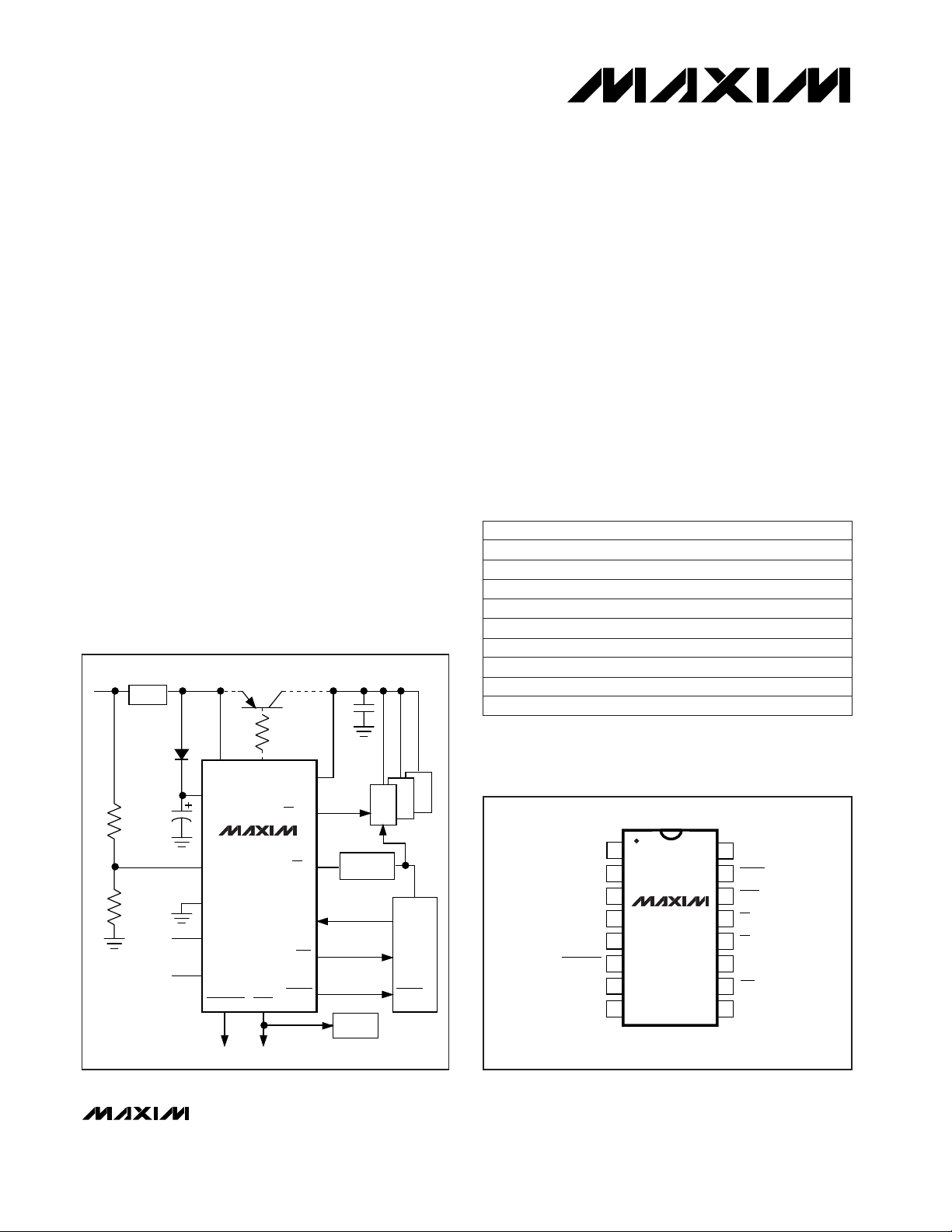
ADDRESS
DECODE
AUDIBLE
ALARM
5V
REGULATOR
+8V
0.1µF
CMOS RAM
2
12
11
10
15
13
5
3
A0-A15
I/O
NMI
RESET
µP
LOW LINE WDO
SYSTEM STATUS INDICATORS
NO
CONNECTION
0.47F*
1N4148
*MaxCap
614
__________Typical Operating Circuit
19-0094; Rev 7a; 12/96
PART
MAX691ACPE
MAX691ACSE
MAX691ACWE 0°C to +70°C
0°C to +70°C
0°C to +70°C
TEMP. RANGE PIN-PACKAGE
16 Plastic DIP
16 Narrow SO
16 Wide SO
MAX691AC/D
MAX691AEJE -40°C to +85°C
0°C to +70°C Dice*
16 CERDIP
MAX691AEPE
MAX691AESE -40°C to +85°C
-40°C to +85°C 16 Plastic DIP
16 Narrow SO
MAX691AEWE -40°C to +85°C 16 Wide SO
MAX691AMJE -55°C to +125°C 16 CERDIP
SuperCap is a registered trademark of Baknor Industries. MaxCap is a registered trademark of The Carborundum Corp.
For free samples & the latest literature: http://www.maxim-ic.com, or phone 1-800-998-8800.
For small orders, phone 408-737-7600 ext. 3468.
TA= T
MIN
+ T
MIN
MAX691A/MAX693A/MAX800L/MAX800M
Microprocessor Supervisory Circuits
2 _______________________________________________________________________________________
ABSOLUTE MAXIMUM RATINGS
ELECTRICAL CHARACTERISTICS
(MAX691A, MAX800L: VCC= +4.75V to +5.5V, MAX693A, MAX800M: VCC= +4.5V to +5.5V, VBATT = 2.8V, TA= T
MIN
to T
MAX
,
unless otherwise noted.)
Stresses beyond those listed under “Absolute Maximum Ratings” may cause permanent damage to the device. These are stress ratings only, and functional
operation of the device at these or any other conditions beyond those indicated in the operational sections of the specifications is not implied. Exposure to
absolute maximum rating conditions for extended periods may affect device reliability.
Terminal Voltage (with respect to GND)
V
CC
.......................................................................-0.3V to +6V
VBATT...................................................................-0.3V to +6V
All Other Inputs.....................................-0.3V to (V
OUT
+ 0.3V)
Input Current
V
CC
Peak...........................................................................1.0A
V
CC
Continuous.............................................................250mA
VBATT Peak..................................................................250mA
VBATT Continuous..........................................................25mA
GND, BATT ON.............................................................100mA
All Other Outputs ............................................................25mA
Continuous Power Dissipation (T
A
= +70°C)
Plastic DIP (derate 10.53mW/°C above +70°C) ..........842mW
Narrow SO (derate 8.70mW/°C above +70°C) ...........696mW
Wide SO (derate 9.52mW/°C above +70°C)...............762mW
CERDIP (derate 10.00mW/°C above +70°C)..............800mW
Operating Temperature Ranges
MAX69_AC_ _/MAX800_C_ _ .............................0°C to +70°C
MAX69_AE_ _/MAX800_E_ _...........................-40°C to +85°C
MAX69_AMJE................................................-55°C to +125°C
Storage Temperature Range.............................-65°C to +160°C
Lead Temperature (soldering, 10sec).............................+300°C
VBATT - 0.15
MAX69_AC, MAX800_C 0.8 1.2
VBATT = 4.5V, IOUT = 20mA
µA
-1.0 0.02
VBATT + 0.2V ≤ V
CC
VBATT Standby Current
(Note 3)
-0.1 0.02
µA
5
VCC< VBATT - 1.2V
VBATT = 2.8V
Supply Current in
Battery-Backup Mode
(Excludes I
OUT
) (Note 2)
VBATT = 2.8V, IOUT = 10mA
V0 5.5
CONDITIONS
Operating Voltage Range,
V
CC
, VBATT (Note 1)
VBATT = 4.5V
0.04 1
µA30 100
Supply Current in
Normal Operating Mode
(Excludes I
OUT
)
V
V
OUT
in Battery-Backup
Mode
VBATT - 0.25
VBATT = 2.8V Ω
30
VBATT - 0.3
VBATT-to-V
OUT
On-Resistance
UNITSMIN TYP MAXPARAMETER
25
TA= +25°C
VCC> VBATT - 1V
TA= T
MIN
+ T
MIN
VBATT = 2.0V, IOUT = 5mA
TA= +25°C
TA= T
MIN
+ T
MIN
15
VBATT = 2.0V
VCC= 4.5V
I
OUT
= 250mA
VCC- 0.02 VCC- 0.05I
OUT
= 25mA
MAX69_AC/AE,
MAX800_C/E
I
OUT
= 210mA
VCC- 0.2 VCC- 0.35
VCC- 0.2 VCC- 0.3
V
VCC- 0.40
VCC- 0.17 VCC- 0.3V
V
OUT
Output
MAX69_AE,
MAX800_C/E
MAX69_AC
MAX69_A/M
MAX69_AE, MAX800_E 0.8 1.4
MAX69_A/M 0.8 1.6
ΩVCC= 4.5VVCC-to-V
OUT
On-Resistance
V
VBATT - 0.3
Power-up
Battery Switchover
Threshold
VBATT + 0.3
Power-down

MAX691A/MAX693A/MAX800L/MAX800M
Microprocessor Supervisory Circuits
_______________________________________________________________________________________ 3
MAX691A, MAX800L
mA7 20
–
RESET Output Short-Circuit
Current
V
3.5
RESET Output Voltage
0.1 0.4
0.004 0.3
ns100
Minimum Watchdog Input
Pulse Width
Clock
Cycles
1024
Watchdog Timeout Period,
External Clock (Note 4)
4096
ms70 100 140
Watchdog Timeout Period,
Internal Oscillator
1.0 1.6 2.25
Clock
Cycles
2048
Reset Active Timeout Period,
External Clock (Note 4)
ms140 200 280
Reset Active Timeout Period,
Internal Oscillator
ns800
LOW LINE-to-RESET Delay
µs80VCCto RESET Delay
MAX693A, MAX800M
CONDITIONS
mV15Reset Threshold Hysteresis
V
4.30 4.45
Reset Threshold Voltage
4.55 4.70
4.25 4.40 4.50
4.50 4.65 4.75
UNITSMIN TYP MAXPARAMETER
Output source current
I
SOURCE
= 1.6mA, VCC= 5V
I
SINK
= 3.2mA, VCC= 4.25V
I
SINK
= 50µA, VCC= 1V, VBATT = 0V, VCCfalling
VIL= 0.8V, VIH= 0.75 x V
CC
Short period
Long period
Short period
Long period
MAX800M, TA= +25°C, VCCfalling
Power-up
Power-up
MAX800L, TA= +25°C, VCCfalling
Power-down
ELECTRICAL CHARACTERISTICS (continued)
(MAX691A, MAX800L: VCC= +4.75V to +5.5V, MAX693A, MAX800M: VCC= +4.5V to +5.5V, VBATT = 2.8V, TA= T
MIN
to T
MAX
,
unless otherwise noted.)
RESET Output Voltage Low
(Note 5)
I
SINK
= 3.2mA 0.1 0.4 V
I
SINK
= 3.2mA, VCC= 4.25V 0.4
LOW LINE Output Voltage
I
SOURCE
= 1µA, VCC= 5V 3.5
V
LOW LINE Output
Short-Circuit Current
Output source current 1 15 100 µA
I
SINK
= 3.2mA 0.4
WDO Output Voltage
I
SOURCE
= 500µA, VCC= 5V 3.5
V
WDO Output
Short-Circuit Current
Output source current 3 10 mA
V
IH
0.75 x V
CC
WDI Threshold Voltage
(Note 6)
V
IL
0.8
V
WDI = 0V -50 -10
WDI Input Current
WDI = V
OUT
20 50
µA
sec
mV60
Battery Switchover
Hysteresis
I
SINK
= 25mA
V
0.7 1.5
BATT ON Output
Low Voltage
I
SINK
= 3.2mA 0.1 0.4
Source current µA1 15 100
BATT ON Output
Short-Circuit Current
Sink current mA60
RESET AND WATCHDOG TIMER
MAX691A/MAX693A/MAX800L/MAX800M
Microprocessor Supervisory Circuits
4 _______________________________________________________________________________________
MAX69_AC/AE/AM, VCC= 5V
µA0.10 ±5OSC IN Leakage Current
µs12
RESET-to-CE OUT Delay
2.7
CE OUT Output Voltage High
(Reset Active)
3.5
ns6 10
CE IN-to-CE OUT Propagation
Delay (Note 8)
mA0.1 0.75 2.0
CE OUT Short-Circuit Current
(Reset Active)
Ω75 150
CE IN-to-CE OUT Resistance
(Note 7)
µA±0.005 ±1
CE IN Leakage Current
60
PFI-to-PFO Delay µs
25
µA1 15 100
PFO Output Short-Circuit
Current
MAX800_C/E, VCC= 5V
CONDITIONS
3.5
PFO Output Voltage
V
0.4
nA±0.01 ±25PFI Leakage Current
1.225 1.25 1.275
PFI Input Threshold V
1.2 1.25 1.3
UNITSMIN TYP MAXPARAMETER
OSC SEL = 0V
Power-down
VCC= 0V, VBATT = 2.8V, I
OUT
= 1µA
VCC= 5V, I
OUT
= -100µA
50Ω source impedance driver, C
LOAD
= 50pF
Disable mode, –CE OUT = 0V
Enable mode
Disable mode
I
SOURCE
= 1µA, VCC= 5V
I
SINK
= 3.2mA
VIN= 20mV, VOD= 15mV
VIN= -20mV, VOD= 15mV
Output source current
Note 1: Either VCCor VBATT can go to 0V, if the other is greater than 2.0V.
Note 2: The supply current drawn by the MAX691A/MAX800L/MAX800M from the battery excluding I
OUT
typically goes to 10µA
when (VBATT - 1V) < V
CC
< VBATT. In most applications, this is a brief period as VCCfalls through this region.
Note 3: “+” = battery-discharging current, “--” = battery-charging current.
Note 4: Although presented as typical values, the number of clock cycles for the reset and watchdog timeout periods are fixed and
do not vary with process or temperature.
Note 5: RESET is an open-drain output and sinks current only.
Note 6: WDI is internally connected to a voltage divider between V
OUT
and GND. If unconnected, WDI is driven to 1.6V (typ),
disabling the watchdog function.
Note 7: The chip-enable resistance is tested with V
CC
= +4.75V for the MAX691A/MAX800L and VCC= +4.5V for the
MAX693A/MAX800M. CE IN = CE OUT = V
CC
/ 2.
Note 8: The chip-enable propagation delay is measured from the 50% point at CE IN to the 50% point at CE OUT.
ELECTRICAL CHARACTERISTICS (continued)
(MAX691A, MAX800L: VCC= +4.75V to +5.5V, MAX693A, MAX800M: VCC= +4.5V to +5.5V, VBATT = 2.8V, TA= T
MIN
to T
MAX
,
unless otherwise noted.)
kHz50OSC IN Frequency Range
µA10 100OSC SEL Input Pull-Up Current
µA10 100OSC IN Input Pull-Up Current
OSC SEL = 0V
OSC SEL = 0V
OSC SEL = V
OUT
or floating, OSC IN = 0V
V
V
OUT
- 0.3 V
OUT
- 0.6V
IH
3.65 2.00
OSC IN External Oscillator
Threshold Voltage
V
IL
kHz100
OSC IN Frequency with
External Capacitor
OSC SEL = 0V, COSC = 47pF
V
POWER-FAIL COMPARATOR
CHIP-ENABLE GATING
INTERNAL OSCILLATOR
MAX691A/MAX693A/MAX800L/MAX800M
Microprocessor Supervisory Circuits
_______________________________________________________________________________________
5
36
26
-60 120 150
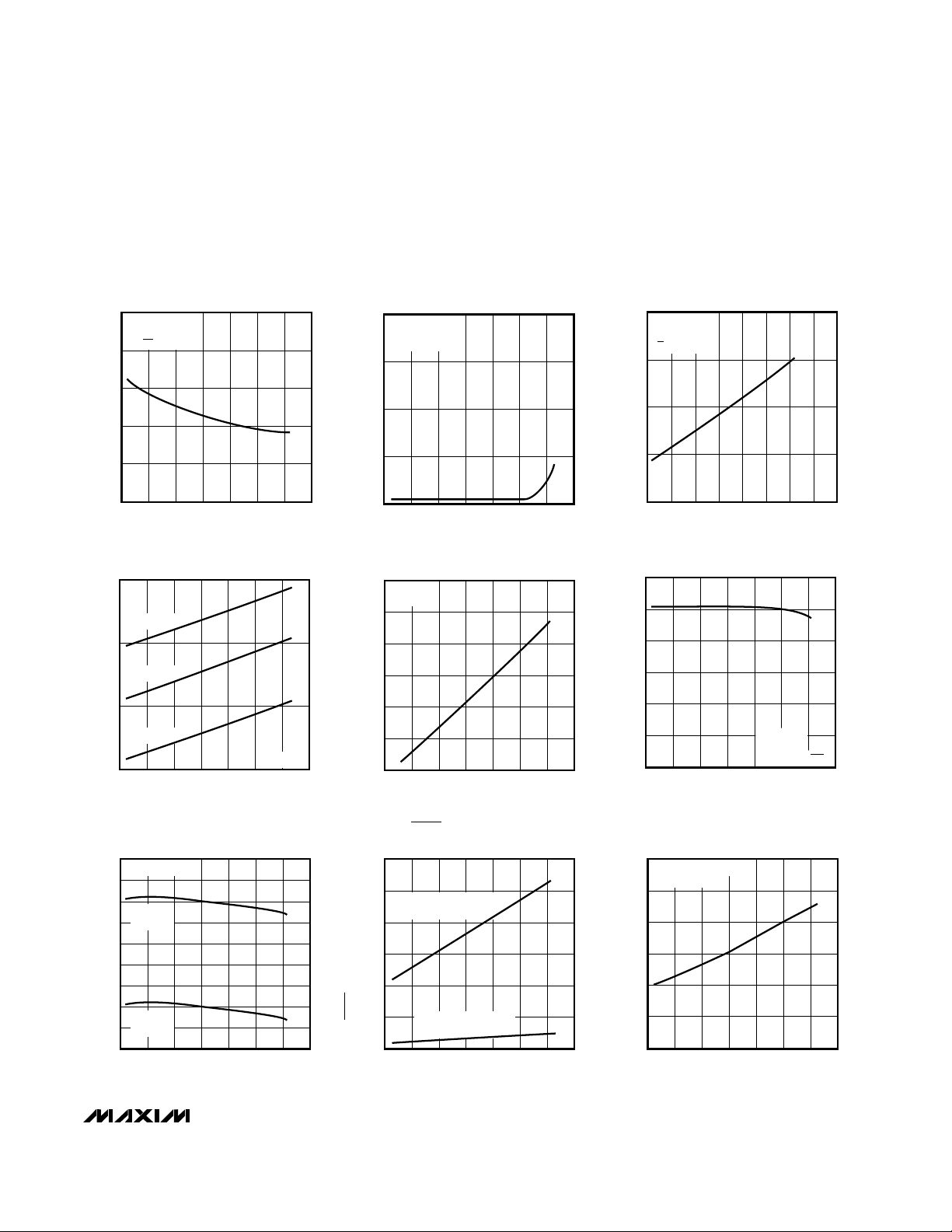
VCC SUPPLY CURRENT
vs. TEMPERATURE
(NORMAL OPERATING MODE)
34
MAX691A TOC-01
TEMPERATURE (°C)
V
CC
SUPPLY CURRENT (µA)
30
30
28
-30 0 90
32
60
V
CC
= 5V
VBATT = 2.8V
PFI, CE IN = 0V
0
-60 120 150
BATTERY SUPPLY CURRENT
vs. TEMPERATURE
(BATTERY-BACKUP MODE)
2
MAX691A TOC-02
TEMPERATURE (°C)
BATTERY SUPPLY CURRENT (µA)
30
1
0.5
-30 0 90
1.5
60
V
CC
= 5V
VBATT = 2.8V
NO LOAD
120
-60 120 150 180
CHIP-ENABLE ON-RESISTANCE
vs. TEMPERATURE
100
MAX691A TOC-03
TEMPERATURE (°C)
CE ON-RESISTANCE (Ω)
30
60
40
-30 0 90
80
60
V
CC
= 4.75V
VBATT = 2.8V
V
CE IN
= VCC/2
20
5
-60 120 150
VBATT to V
OUT
ON-RESISTANCE
vs. TEMPERATURE
MAX691A TOC-04
TEMPERATURE (°C)
VBATT-to-V
OUT
ON-RESISTANCE (Ω)
30
10
-30 0 90
15
60
V
CC
= 0V
VBATT = 2.8V
VBATT = 2.0V
VBATT = 4.5V
4.75
4.30
-60 120 150
RESET THRESHOLD
vs. TEMPERATURE
MAX691A TOC-07
TEMPERATURE (°C)
RESET THRESHOLD (V)
30
4.45
-30 0 90
4.65
4.40
4.35
4.50
4.70
4.55
4.60
60
VBATT = 2.8V
MAX691A
MAX800L
MAX693A
MAX800M
1.2
0.6
-60 120 150
V
CC
to V
OUT
ON-RESISTANCE
vs. TEMPERATURE
MAX691A TOC-05
TEMPERATURE (°C)
V
CC
-to-V
OUT
ON-RESISTANCE (Ω)
30
0.8
-30 0 90
1.0
0.7
0.9
1.1
60
VCC = 5V,
VBATT = 0V
1.50
0
-60 120 150
PFI THRESHOLD
vs. TEMPERATURE
MAX691A TOC-06
TEMPERATURE (°C)
PFI THRESHOLD (V)
30
0.50
-30 0 90
1.00
0.25
0.75
1.25
60
VCC = +5V,
VBATT = 0V
NO LOAD ON PFO
600
0
-60 120 150
RESET OUTPUT RESISTANCE
vs. TEMPERATURE
MAX691A TOC-08
TEMPERATURE (°C)
RESET OUTPUT RESISTANCE (Ω)
30
200
-30 0 90
100
500
300
400
60
VCC = 5V, VBATT = 2.8V
SOURCING CURRENT
VCC = 0V, VBATT = 2.8V
SINKING CURRENT
-60 120 150
RESET DELAY
vs. TEMPERATURE
230
MAX691A TOC-09
TEMPERATURE (°C)
RESET DELAY (ms)
30
190
170
-30 0 90
210
220
180
200
60
V
CC
= 0V TO 5V STEP
VBATT = 2.8V
__________________________________________Typical Operating Characteristics
(TA = +25°C, unless otherwise noted.)

MAX691A/MAX693A/MAX800L/MAX800M
Microprocessor Supervisory Circuits
6 _______________________________________________________________________________________
____________________________Typical Operating Characteristics (continued)
(TA = +25°C, unless otherwise noted.)
20
0
0
BATTERY CURRENT
vs. INPUT SUPPLY VOLTAGE
16
MAX691A TOC-10
VCC (V)
I
BATT
(µA)
3
8
4
1 2 5
12
4
VBATT = 2.8V
I
OUT
= 0A
100
0.1
WATCHDOG AND RESET TIMEOUT PERIOD
vs. OSC IN TIMING CAPACITOR (COSC)
10
MAX691A TOC-11
COSC (pF)
WATCHDOG AND RESET TIMEOUT PERIOD (sec)
100
1
10 1000
VCC = 5V
VBATT = 2.8V
LONG WATCHDOG
TIMEOUT PERIOD
SHORT WATCHDOG
TIMEOUT PERIOD
RESET ACTIVE
TIMEOUT PERIOD
0 300
CHIP-ENABLE PROPAGATION DELAY
vs. CE OUT LOAD CAPACITANCE
MAX691A TOC-12
C
LOAD
(pF)
PROPAGATION DELAY (ns)
150
8
0
50 100 250
16
20
4
12
200
V
CC
= 5V
CE IN = 0V TO 5V
DRIVER SOURCE
IMPEDANCE = 50Ω
1000
1
1
V
CC
to V
OUT
vs. OUTPUT CURRENT
(NORMAL OPERATING MODE)
100
MAX691A TOC-13
I
OUT
(mA)
V
CC
to V
OUT
(mV)
100
10
10 1000
VCC = 4.5V
VBATT = 0V
SLOPE = 0.8Ω
1000
1
VBATT to V
OUT
vs. OUTPUT CURRENT
(BATTERY-BACKUP MODE)
100
MAX691A TOC-14
I
OUT
(mA)
VBATT to V
OUT
(mV)
10
10
1 100
VCC = 0V
VBATT = 4.5V
SLOPE = 8Ω
LO
VCC to LOW LINE
AND CE OUT DELAY
MAX691A TOC-15
LOW LINE
5V
V
CC
RESET
THRESHOLD
LO
HI
HI
HI
LO
CE OUT
RESET
12µs
800ns
80µs

MAX691A/MAX693A/MAX800L/MAX800M
Microprocessor Supervisory Circuits
_______________________________________________________________________________________ 7
______________________________________________________________Pin Description
NAME FUNCTION
1 VBATT
Battery-Backup Input. Connect to external battery or capacitor and charging circuit. If backup battery is not
used, connect to GND.
2 V
OUT
Output Supply Voltage. When VCCis greater than VBATT and above the reset threshold, V
OUT
connects to
VCC. When VCCfalls below VBATT and is below the reset threshold, V
OUT
connects to VBATT. Connect a 0.1µF
capacitor from V
OUT
to GND. Connect V
OUT
to VCCif no backup battery is used.
PIN
3 V
CC Input Supply Voltage, 5V input.
4 GND
Ground. 0V reference for all signals.
8 OSC SEL
Oscillator Select. When OSC SEL is unconnected or driven high, the internal oscillator sets the reset delay and
watchdog timeout period. When OSC SEL is low, the external oscillator input (OSC IN) is enabled (Table 1).
OSC SEL has a 10µA internal pull-up.
7 OSC IN
External Oscillator Input. When OSC SEL is unconnected or driven high, a 10µA pull-up connects from V
OUT
to
OSC IN, the internal oscillator sets the reset and watchdog timeout periods, and OSC IN selects between fast
and slow watchdog timeout periods. When OSC SEL is driven low, the reset and watchdog timeout periods may
be set either by a capacitor from OSC IN to ground or by an external clock at OSC IN (Figure 3).
6
LOW LINE
LOW LINE output goes low when VCCfalls below the reset threshold. It returns high as soon as VCCrises above
the reset threshold.
5 BATT ON
Battery On Output. When V
OUT
switches to VBATT, BATT ON goes high. When V
OUT
switches to V
CC,
BATT ON
goes low. Connect the base of a PNP through a current-limiting resistor to BATT ON for V
OUT
current require-
ments greater than 250mA.
13
CE IN
Chip-Enable Input. The input to chip-enable gating circuit. If CE IN is not used, connect CE IN to GND or V
OUT.
12
CE OUT
Chip-Enable Output. CE OUT goes low only when CE IN is low and VCCis above the reset threshold. If CE IN is
low when reset is asserted, CE OUT will stay low for 15µs or until CE IN goes high, whichever occurs first.
11 WDI
Watchdog Input. WDI is a three-level input. If WDI remains either high or low for longer than the watchdog timeout period, WDO goes low and reset is asserted for the reset timeout period. WDO remains low until the next transition at WDI. Leaving WDI unconnected disables the watchdog function. WDI connects to an internal voltage
divider between V
OUT
and GND, which sets it to mid-supply when left unconnected.
10
PFO
Power-Fail Output. This is the output of the power-fail comparator. PFO goes low when PFI is less than 1.25V.
This is an uncommitted comparator, and has no effect on any other internal circuitry.
9 PFI
Power-Fail Input. This is the noninverting input to the power-fail comparator. When PFI is less than 1.25V, PFO
goes low. When PFI is not used, connect PFI to GND or V
OUT
.
16 RESET
RESET is an active-high output. It is open drain, and the inverse of RESET.
15
RESET
RESET Output goes low whenever VCCfalls below the reset threshold. RESET will remain low typically for
200ms after V
CC
crosses the reset threshold on power-up.
14
WDO
Watchdog Output. If WDI remains high or low longer than the watchdog timeout period, WDO goes low and reset
is asserted for the reset timeout period. WDO returns high on the next transition at WDI. WDO remains high if
WDI is unconnected.
_______________Detailed Description
–R—E—S—E—T–
and RESET Outputs
The MAX691A/MAX693A/MAX800L/MAX800M’s RESET
and RESET outputs ensure that the µP (with reset
inputs asserted either high or low) powers up in a
known state, and prevents code-execution errors during power-down or brownout conditions.
The RESET output is active low, and typically sinks
3.2mA at 0.1V saturation voltage in its active state.
When deasserted, –RESET sources 1.6mA at typically
V
OUT
- 0.5V. RESET output is open drain, active high,
and typically sinks 3.2mA with a saturation voltage of
0.1V. When no backup battery is used, RESET output is
guaranteed to be valid down to V
CC
= 1V, and an
external 10kΩ pull-down resistor on RESET insures
that it will be valid with VCCdown to GND (Figure 1).
As VCCgoes below 1V, the gate drive to the RESET
output switch reduces accordingly, increasing the
R
DS(ON)
and the saturation voltage. The 10kΩ pulldown resistor insures the parallel combination of switch
plus resistor is around 10kΩ and the output saturation
voltage is below 0.4V while sinking 40µA. When using
a 10kΩ external pull-down resistor, the high state for
RESET output with VCC= 4.75V will be 4.5V typical.
For battery voltages ≥ 2V connected to VBATT, RESET
and RESET remain valid for VCCfrom 0V to 5.5V.

MAX691A/MAX693A/MAX800L/MAX800M
RESET and RESET are asserted when VCCfalls below
the reset threshold (4.65V for the MAX691A/MAX800L,
4.4V for the MAX693A/MAX800M) and remain asserted
for 200ms typ after VCCrises above the reset threshold
on power-up (Figure 5). The devices’ batteryswitchover comparator does not affect reset assertion.
However, both reset outputs are asserted in batterybackup mode since VCCmust be below the reset
threshold to enter this mode.
Watchdog Function
The watchdog monitors µP activity via the Watchdog
Input (WDI). If the µP becomes inactive, RESET and
RESET are asserted. To use the watchdog function,
connect WDI to a bus line or µP I/O line. If WDI
remains high or low for longer than the watchdog timeout period (1.6sec nominal), WDO, RESET, and RESET
are asserted (see
RESET and RESET Outputs
section,
and the
Watchdog Output
discussion on this page).
Watchdog Input
A change of state (high to low, low to high, or a minimum 100ns pulse) at the WDI during the watchdog
period resets the watchdog timer. The watchdog
default timeout is 1.6sec.
To disable the watchdog function, leave WDI floating.
An internal resistor network (100kΩ equivalent impedance at WDI) biases WDI to approximately 1.6V.
Internal comparators detect this level and disable the
watchdog timer. When VCCis below the reset threshold, the watchdog function is disabled and WDI is disconnected from its internal resistor network, thus
becoming high impedance.
Watchdog Output
The Watchdog Output (WDO) remains high if there is a
transition or pulse at WDI during the watchdog timeout
period. The watchdog function is disabled and –WDO is
a logic high when VCCis below the reset threshold, battery-backup mode is enabled, or WDI is an open circuit.
In watchdog mode, if no transition occurs at WDI during
the watchdog timeout period, RESET and RESET are
asserted for the reset timeout period (200ms typical).
WDO goes low and remains low until the next transition
at WDI (Figure 2). If WDI is held high or low indefinitely,
RESET and RESET will generate 200ms pulses every
1.6sec. WDO has a 2 x TTL output characteristic.
Selecting an Alternative
Watchdog and Reset Timeout Period
The OSC SEL and OSC IN inputs control the watchdog
and reset timeout periods. Floating OSC SEL and OSC
IN or tying them both to V
OUT
selects the nominal 1.6sec
watchdog timeout period and 200ms reset timeout period. Connecting OSC IN to GND and floating or connecting OSC SEL to V
OUT
selects the 100ms normal
watchdog timeout delay and 1.6sec delay immediately
after reset. The reset timeout delay remains 200ms
(Figure 2). Select alternative timeout periods by connecting OSC SEL to GND and connecting a capacitor
between OSC IN and GND, or by externally driving OSC
IN (Table 1 and Figure 3). OSC IN is internally connected to a ±100nA (typ) current source that charges and
discharges the timing capacitor to create the oscillator
frequency, which sets the reset and watchdog timeout
periods (see
Connecting a Timing Capacitor at OSC IN
in the
Applications Information
section).
Microprocessor Supervisory Circuits
8 _______________________________________________________________________________________
MAX691A
MAX693A
TO µP RESET
1k
15
RESET
Figure 1. Adding an external pull-down resistor ensures
–R—E—S—E—T–
is valid with V
CC
down to GND.
Figure 2. Watchdog Timeout Period and Reset Active Time
WDI
WDO
t
2
RESET t
t1 = RESET TIMEOUT PERIOD
= NORMAL WATCHDOG TIMEOUT PERIOD
t
2
= WATCHDOG TIMEOUT PERIOD IMMEDIATELY AFTER RESET
t
3
1
t
1
t
3

MAX691A/MAX693A/MAX800L/MAX800M
Microprocessor Supervisory Circuits
_______________________________________________________________________________________ 9
Chip-Enable Signal Gating
The MAX691A/MAX693A/MAX800L/MAX800M provide
internal gating of chip-enable (CE) signals to prevent
erroneous data from being written to CMOS RAM in the
event of a power failure. During normal operation, the
CE gate is enabled and passes all CE transitions. When
reset is asserted, this path becomes disabled, preventing erroneous data from corrupting the CMOS RAM. All
these parts use a series transmission gate from –CE IN to
CE OUT (Figure 4).
The 10ns max CE propagation delay from CE IN to CE
OUT enables the parts to be used with most µPs.
Chip-Enable Input
The Chip-Enable Input (CE IN) is high impedance (disabled mode) while RESET and –R—E—S—E—T–are asserted.
During a power-down sequence where VCCfalls below
the reset threshold or a watchdog fault, –CE IN assumes
a high-impedance state when the voltage at –CE IN
goes high or 15µs after reset is asserted, whichever
occurs first (Figure 5).
During a power-up sequence, CE IN remains high
impedance, regardless of CE IN activity, until reset is
deasserted following the reset timeout period.
In the high-impedance mode, the leakage currents into
this terminal are ±1µA max over temperature. In the
low-impedance mode, the impedance of –CE IN appears
as a 75Ω resistor in series with the load at CE OUT.
The propagation delay through the CE transmission
gate depends on both the source impedance of the
drive to –CE IN and the capacitive loading on the ChipEnable Output (–CE OUT) (see Chip-Enable Propagation
Delay vs. CE OUT Load Capacitance in the
Typical
Operating Characteristics
). The CE propagation delay
is production tested from the 50% point of –CE IN to the
50% point of –CE OUT using a 50Ω driver and 50pF of
load capacitance (Figure 6). For minimum propagation
delay, minimize the capacitive load at CE OUT, and
use a low output-impedance driver.
Chip-Enable Output
In the enabled mode, the impedance of CE OUT is
equivalent to 75Ω in series with the source driving CE
IN. In the disabled mode, the 75Ω transmission gate is
off and CE OUT is actively pulled to V
OUT
. This source
turns off when the transmission gate is enabled.
–L—O—W——L—I—N—E–
Output
LOW LINE is the buffered output of the reset threshold
comparator. LOW LINE typically sinks 3.2mA at 0.1V.
For normal operation (VCCabove the LOW LINE threshold), LOW LINE is pulled to V
OUT
.
Power-Fail Comparator
The power-fail comparator is an uncommitted comparator
that has no effect on the other functions of the IC.
Common uses include low-battery indication (Figure 7),
and early power-fail warning (see
Typical Operating
Circuit
).
Power-Fail Input
Power Fail Input (PFI) is the input to the power-fail comparator. It has a guaranteed input leakage of ±25nA
max over temperature. The typical comparator delay is
25µs from VILto VOL(power failing), and 60µs from V
IH
to VOH(power being restored). If PFI is not used, connect it to ground.
OSC SEL
OSC IN
7
8
EXTERNAL
OSCILLATOR
OSC SEL
OSC IN
7
8
EXTERNAL
CLOCK
OSC SEL
OSC IN
7
8
INTERNAL OSCILLATOR
100ms WATCHDOG
OSC SEL
OSC IN
7
8
INTERNAL OSCILLATOR
1.6sec WATCHDOG
MAX691A
MAX693A
MAX800L
MAX800M
N.C. N.C.
N.C.
50kHz
Figure 3. Oscillator Circuits
Watchdog Timeout Period
OSC SEL OSC IN
Normal Immediately After Reset
Reset Timeout Period
Low External Clock Input 1024 clks 4096 clks 2048 clks
Low External Capacitor (600/47pF x C)ms (2.4/47pF x C)sec (1200/47pF x C)ms
Floating Low 100ms 1.6sec 200ms
Floating Floating 1.6sec 1.6sec 200ms
Table 1. Reset Pulse Width and Watchdog Timeout Selections

MAX691A/MAX693A/MAX800L/MAX800M
Microprocessor Supervisory Circuits
10 ______________________________________________________________________________________
MAX691A
MAX693A
MAX800L
MAX800M
CHIP-ENABLE
OUTPUT
CONTROL
V
CC
3
1
13
7
11
9
VBATT
CE IN
OSC IN
WDI
PFI
RESET
GENERATOR
TIMEBASE FOR
RESET AND
WATCHDOG
WATCHDOG
TRANSITION
DETECTOR
WATCHDOG
TIMER
8
OSC SEL
1.25V
GND
4
4.65V*
6
LOW LINE
5
2
12
15
16
14
PFO
WDO
RESET
RESET
CE OUT
10
V
OUT
BATT ON
* 4.4V FOR THE MAX693A/MAX800M
Figure 4. MAX691A/MAX693A/MAX800L/MAX800M Block Diagram
Figure 5. Reset and Chip-Enable Timing
5.0V
4.0V
5.0V
0V
5V
0V
5V
0V
5V
0V
LOGIC LEVELS SHOWN ARE FROM 0V TO 5V.
V
RESET
THRESHOLD
CE IN
CE OUT
RESET
RESET
CC
15µs
100µs
100µs

MAX691A/MAX693A/MAX800L/MAX800M
Microprocessor Supervisory Circuits
______________________________________________________________________________________ 11
Power-Fail Output
The Power-Fail Output (PFO) goes low when PFI goes
below 1.25V. It typically sinks 3.2mA with a saturation
voltage of 0.1V. With PFI above 1.25V, PFO is actively
pulled to V
OUT
.
Battery-Backup Mode
Two conditions are required to switch to battery-backup mode: 1) VCCmust be below the reset threshold,
and 2) VCCmust be below VBATT. Table 2 lists the status of the inputs and outputs in battery-backup mode.
Battery On Output
The Battery On (BATT ON) output indicates the status
of the internal VCC/battery-switchover comparator,
which controls the internal VCCand VBATT switches.
For VCCgreater than VBATT (ignoring the small hysteresis effect), BATT ON typically sinks 3.2mA at 0.1V
saturation voltage. In battery-backup mode, this terminal sources approximately 10µA from V
OUT
. Use BATT
ON to indicate battery-switchover status or to supply
base drive to an external pass transistor for higher-current applications (see
Typical Operating Circuit
).
Input Supply Voltage
The Input Supply Voltage (VCC) should be a regulated
5V. VCCconnects to V
OUT
via a parallel diode and a
large PMOS switch. The switch carries the entire current load for currents less than 250mA. The parallel
diode carries any current in excess of 250mA. Both the
switch and the diode have impedances less than 1Ω
each. The maximum continuous current is 250mA, but
power-on transients may reach a maximum of 1A.
MAX691A
MAX693A
MAX800L
MAX800M
CE IN
C
LOAD
CE OUT
GND
+5V
50Ω
OUTPUT
IMPEDANCE
V
CC
VBATT
2.8V
Figure 6. CE Propagation Delay Test Circuit Figure 7. Low-Battery Indicator
PIN NAME STATUS
1 VBATT Supply current is 1µA max.
2 V
OUT
V
OUT
is connected to VBATT through an
internal PMOS switch.
3 V
CC
Battery switchover comparator monitors
VCCfor active switchover.
4 GND GND 0V, 0V reference for all signals.
5 BATT ON
Logic high. The open-circuit output is
equal to V
OUT
.
6
LOWLINE
Logic low*
7 OSC IN OSC IN is ignored.
8 OSC SEL OSC SEL is ignored.
9 PFI
The power-fail comparator remains
active in the battery-backup mode for
VCC≥ VBATT - 1.2V typ.
10
PFO
The power-fail comparator remains
active in the battery-backup mode for
VCC≥ VBATT - 1.2V typ. Below this volt-
age, PFO is forced low.
11 WDI Watchdog is ignored.
12
CE OUT
Logic high. The open-circuit voltage is
equal to V
OUT
.
13
CE IN
High impedance
14
WDO
Logic high. The open-circuit voltage is
equal to V
OUT
.
15
RESET
Logic low*
16 RESET High impedance*
Table 2. Input and Output Status in Battery-Backup
Mode
* VCCmust be below the reset threshold to enter battery-backup
mode.
2.0V to 5.5V
+5V
V
CC
VBATT
MAX691A
MAX693A
MAX800L
PFI
MAX800M
PFO
GND
LOW BATT

MAX691A/MAX693A/MAX800L/MAX800M
Battery-Backup Input
The Battery-Backup Input (VBATT) is similar to the V
CC
input except the PMOS switch and parallel diode are
much smaller. Accordingly, the on-resistances of the
diode and the switch are each approximately 10Ω.
Continuous current should be limited to 25mA and
peak currents (only during power-up) limited to 250mA.
The reverse leakage of this input is less than 1µA over
temperature and supply voltage (Figure 8).
Output Supply Voltage
The Output Supply Voltage (V
OUT
) pin is internally connected to the substrate of the IC and supplies current
to the external system and internal circuitry. All opencircuit outputs will, for example, assume the V
OUT
voltage in their high states rather than the VCCvoltage. At
the maximum source current of 250mA, V
OUT
will typically be 200mV below VCC. Decouple this terminal with
a 0.1µF capacitor.
__________Applications Information
The MAX691A/MAX693A/MAX800L/MAX800M are not
short-circuit protected. Shorting V
OUT
to ground, other
than power-up transients such as charging a decoupling capacitor, destroys the device.
All open-circuit outputs swing between V
OUT
and GND
rather than VCCand GND.
If long leads connect to the chip inputs, insure that
these leads are free from ringing and other conditions
that would forward bias the chip’s protection diodes.
There are three distinct modes of operation:
1) Normal operating mode with all circuitry powered
up. Typical supply current from V
CC
is 35µA while
only leakage currents flow from the battery.
2) Battery-backup mode where VCCis typically within
0.7V below VBATT. All circuitry is powered up
and the supply current from the battery is typically
less than 60µA.
3) Battery-backup mode where VCCis less than
VBATT by at least 0.7V. VBATT supply current is
1µA max.
Using SuperCap™ or MaxCap™ with the
MAX691A/MAX693A/MAX800L/MAX800M
VBATT has the same operating voltage range as VCC,
and the battery switchover threshold voltages are typically ±30mV centered at VBATT, allowing use of a
SuperCap and a simple charging circuit as a backup
source (Figure 9).
If VCCis above the reset threshold and VBATT is 0.5V
above VCC, current flows to V
OUT
and VCCfrom VBATT
until the voltage at VBATT is less than 0.5V above VCC.
For example, with a SuperCap connected to VBATT and
through a diode to VCC, if VCCquickly changes from 5.4V
to 4.9V, the capacitor discharges through V
OUT
and V
CC
until VBATT reaches 5.1V typ. Leakage current through
the SuperCap charging diode and the internal power
diode eventually discharges the SuperCap to VCC. Also, if
VCCand VBATT start from 0.1V above the reset threshold
and power is lost at VCC, the SuperCap on VBATT discharges through VCCuntil VBATT reaches the reset
threshold; then the battery-backup mode is initiated and
the current through VCCgoes to zero.
Microprocessor Supervisory Circuits
12 ______________________________________________________________________________________
MAX691A
MAX693A
MAX800L
MAX800M
VBATT
V
CC
0.1µF
V
OUT
Figure 8. VCCand VBATT to V
OUT
Switch Figure 9. SuperCap or MaxCap on VBATT
+5V
1N4148
1
VBATT
0.47F*
* MaxCap
MAX691A
MAX693A
MAX800L
MAX800M
V
GND
3
CC
2
V
OUT
4

Using Separate Power Supplies
for VBATT and V
CC
If using separate power supplies for VCCand VBATT,
VBATT must be less than 0.3V above VCCwhen VCCis
above the reset threshold. As described in the previous section, if VBATT exceeds this limit and power is
lost at VCC, current flows continuously from VBATT to
VCCvia the VBATT-to-V
OUT
diode and the V
OUT
-to-V
CC
switch until the circuit is broken (Figure 8).
Alternate Chip-Enable Gating
Using memory devices with both CE and CE inputs
allows the CE loop to be bypassed. To do this, connect CE IN to ground, pull up CE OUT to V
OUT
, and
connect –CE OUT to the CE input of each memory
device (Figure 10). The CE input of each part then
connects directly to the chip-select logic, which does
not have to be gated.
Adding Hysteresis to the
Power-Fail Comparator
Hysteresis adds a noise margin to the power-fail comparator and prevents repeated triggering of PFO when
VINis near the power-fail comparator trip point. Figure
11 shows how to add hysteresis to the power-fail com-
MAX691A/MAX693A/MAX800L/MAX800M
Microprocessor Supervisory Circuits
______________________________________________________________________________________ 13
MAX691A
MAX693A
MAX800L
MAX800M
V
OUT
GND
CE IN
CE
CE
CE OUT
CE
CE
CE
CE
CE
CE
*MAXIMUM Rp VALUE DEPENDS ON
THE NUMBER OF RAMS.
MINIMUM Rp VALUE IS 1kΩ.
ACTIVE-HIGH
CE LINES
FROM LOGIC
RAM 1
RAM 2
RAM 3
RAM 4
Rp*
MAX691A
MAX693A
MAX800L
MAX800M
V
CC
GND
PFI
R2
R1
+5V
PFO
PFO
5V
0V
NOTE: V
TRIP
IS NEGATIVE
0V
V
TRIP
V-
5 - 1.25 = 1.25 - V
TRIP
R1 R2
V-
Figure 10. Alternate CE Gating
Figure 12. Monitoring a Negative Voltage
Figure 11. Adding Hysteresis to the Power-Fail Comparator
V
IN
R1
C1*
R2
5V
PFO
0V
0V V
= 1.25
V
TRIP
R2
= 1.25/
V
H
R1 + R2 I I R3 R1 R3 R2
R3
TO µP
R1 + R2
R2 I I R3 VL - 1.25 + 5 - 1.25 = 1.25
PFI
PFO
+5V
V
CC
MAX691A
MAX693A
MAX800L
MAX800M
GND
V
V
TRIP
L
V
IN
*OPTIONAL
H

MAX691A/MAX693A/MAX800L/MAX800M
Microprocessor Supervisory Circuits
14 ______________________________________________________________________________________
parator. Select the ratio of R1 and R2 such that PFI sees
1.25V when VINfalls to the desired trip point (V
TRIP
).
Resistor R3 adds hysteresis. It will typically be an order
of magnitude greater than R1 or R2. The current
through R1 and R2 should be at least 1µA to ensure that
the 25nA (max) PFI input current does not shift the trip
point. R3 should be larger than 10kΩ to prevent it from
loading down the PFO pin. Capacitor C1 adds noise
rejection.
Monitoring a Negative Voltage
The power-fail comparator can be used to monitor a
negative supply voltage using Figure 12’s circuit. When
the negative supply is valid, PFO is low. When the negative supply voltage drops, PFO goes high. This circuit’s accuracy is affected by the PFI threshold
tolerance, the VCCvoltage, and resistors R1 and R2.
Backup-Battery Replacement
The backup battery may be disconnected while VCCis
above the reset threshold. No precautions are necessary to avoid spurious reset pulses.
Negative-Going VCCTransients
While issuing resets to the µP during power-up, powerdown, and brownout conditions, these supervisors are
relatively immune to short-duration, negative-going V
CC
transients (glitches). It is usually undesirable to reset
the µP when VCCexperiences only small glitches.
Figure 13 shows maximum transient duration vs. resetcomparator overdrive, for which reset pulses are not
generated. The graph was produced using negativegoing VCCpulses, starting at 5V and ending below the
reset threshold by the magnitude indicated (reset comparator overdrive). The graph shows the maximum
pulse width a negative-going VCCtransient may typically have without causing a reset pulse to be issued. As
the amplitude of the transient increases (i.e., goes farther below the reset threshold), the maximum allowable
pulse width decreases. Typically, a VCCtransient that
goes 100mV below the reset threshold and lasts for
40µs or less will not cause a reset pulse to be issued.
A 100nF bypass capacitor mounted close to the V
CC
pin provides additional transient immunity.
Connecting a Timing Capacitor at OSC IN
When OSC SEL is connected to ground, OSC IN disconnects from its internal 10µA (typ) pull-up and is
internally connected to a ±100nA current source.
When a capacitor is connected from OSC IN to ground
(to select alternative reset and watchdog timeout periods), the current source charges and discharges the
timing capacitor to create the oscillator that controls the
reset and watchdog timeout period. To prevent timing
errors or oscillator start-up problems, minimize external
current leakage sources at this pin, and locate the
capacitor as close to OSC IN as possible. The sum of
PC-board leakage plus OSC capacitor leakage must be
small compared to ±100nA.
100
0
10 1000 10000
40
20
80
60
MAX791-16
RESET COMPARATOR OVERDRIVE,
(Reset Threshold Voltage - V
CC
) (mV)
MAXIMUM TRANSIENT DURATION (µs)
100
VCC = 5V
T
A
= +25°C
0.1µF CAPACITOR
FROM V
OUT
TO GND
Figure 13. Maximum Transient Duration without Causing a
Reset Pulse vs. Reset Comparator Overdrive

MAX691A/MAX693A/MAX800L/MAX800M
Microprocessor Supervisory Circuits
______________________________________________________________________________________ 15
Maximum VCCFall Time
The VCCfall time is limited by the propagation delay of
the battery switchover comparator and should not
exceed 0.03V/µs. A standard rule of thumb for filter
capacitance on most regulators is on the order of 100µF
per amp of current. When the power supply is shut off or
the main battery is disconnected, the associated initial
VCCfall rate is just the inverse or 1A/100µF = 0.01V/µs.
The VCCfall rate decreases with time as VCCfalls exponentially, which more than satisfies the maximum fall-time
requirement.
Watchdog Software Considerations
A way to help the watchdog timer keep a closer watch
on software execution involves setting and resetting the
watchdog input at different points in the program,
rather than “pulsing” the watchdog input high-low-high
or low-high-low. This technique avoids a “stuck” loop
where the watchdog timer continues to be reset within
the loop, keeping the watchdog from timing out. Figure
14 shows an example flow diagram where the I/O driving the watchdog input is set high at the beginning of
the program, set low at the beginning of every subroutine or loop, then set high again when the program
returns to the beginning. If the program should “hang”
in any subroutine, the I/O is continually set low and the
watchdog timer is allowed to time out, causing a reset
or interrupt to be issued.
START
SET
WDI
LOW
RETURN
END
SUBROUTINE
OR PROGRAM LOOP
SET WDI
HIGH
Figure 14. Watchdog Flow Diagram

MAX691A/MAX693A/MAX800L/MAX800M
Microprocessor Supervisory Circuits
_Ordering Information (continued)
________________________________________________________Package Information
PART
MAX693ACPE
MAX693ACSE
MAX693ACWE 0°C to +70°C
0°C to +70°C
0°C to +70°C
TEMP. RANGE PIN-PACKAGE
16 Plastic DIP
16 Narrow SO
16 Wide SO
MAX693AC/D
MAX693AEJE -40°C to +85°C
0°C to +70°C Dice*
16 CERDIP
MAX693AEPE
MAX693AESE -40°C to +85°C
-40°C to +85°C 16 Plastic SO
16 Narrow SO
MAX693AEWE -40°C to +85°C 16 Wide SO
MAX693AMJE -55°C to +125°C 16 CERDIP
MAX800LCPE
MAX800LCSE
MAX800LEPE -40°C to +85°C
0°C to +70°C
0°C to +70°C 16 Plastic DIP
16 Narrow SO
16 Plastic DIP
MAX800LESE
MAX800MCPE
MAX800MCSE
-40°C to +85°C 16 Narrow SO
MAX800MEPE -40°C to +85°C
0°C to +70°C
0°C to +70°C 16 Plastic DIP
16 Narrow SO
16 Plastic DIP
MAX800MESE -40°C to +85°C 16 Narrow SO
* Dice are specified at TA= +25°C, DC parameters only.
___________________Chip Topography
WDI
CE IN
CE OUT
V
CC
GND
WDO
BATT ON
LOW LINE
V
OUT
VBATT RESET RESET
PFI PFO
OSC SEL
OSC IN
0.11"
(2.794mm)
0.07"
(1.778mm)
TRANSISTOR COUNT: 729
SUBSTRATE CONNECTED TO V
OUT
SOICN.EPS
Maxim cannot assume responsibility for use of any circuitry other than circuitry entirely embodied in a Maxim product. No circuit patent licenses are
implied. Maxim reserves the right to change the circuitry and specifications without notice at any time.
16
____________________Maxim Integrated Products, 120 San Gabriel Drive, Sunnyvale, CA 94086 408-737-7600
© 1996 Maxim Integrated Products Printed USA is a registered trademark of Maxim Integrated Products.
 Loading...