

Page 1
General Description
The MAX6314 low-power CMOS microprocessor (µP)
supervisory circuit is designed to monitor power
supplies in µP and digital systems. The MAX6314’s
RESET output is bidirectional, allowing it to be directly
connected to µPs with bidirectional reset inputs, such
as the 68HC11. It provides excellent circuit reliability
and low cost by eliminating external components and
adjustments. The MAX6314 also provides a debounced
manual reset input.
This device performs a single function: it asserts a reset
signal whenever the VCCsupply voltage falls below a
preset threshold or whenever manual reset is
asserted. Reset remains asserted for an internally programmed interval (reset timeout period) after VCChas
risen above the reset threshold or manual reset is
deasserted.
The MAX6314 comes with factory-trimmed reset
threshold voltages in 100mV increments from 2.5V
to 5V. Preset timeout periods of 1ms, 20ms, 140ms,
and 1120ms (minimum) are also available. The device
comes in a SOT143 package.
For a µP supervisor with an open-drain reset pin, see
the MAX6315 data sheet.
________________________Applications
Computers
Controllers
Intelligent Instruments
Critical µP and µC Power Monitoring
Portable/Battery-Powered Equipment
Features
♦ Small SOT143 Package
♦ RESET Output Simplifies Interface to
Bidirectional Reset I/Os
♦ Precision Factory-Set VCCReset Thresholds:
100mV Increments from 2.5V to 5V
♦ ±1.8% Reset Threshold Accuracy at TA= +25°C
♦ ±2.5% Reset Threshold Accuracy Over Temp.
♦ Four Reset Timeout Periods Available:
1ms, 20ms, 140ms, or 1120ms (minimum)
♦ Immune to Short VCCTransients
♦ 5µA Supply Current
♦ Pin-Compatible with MAX811
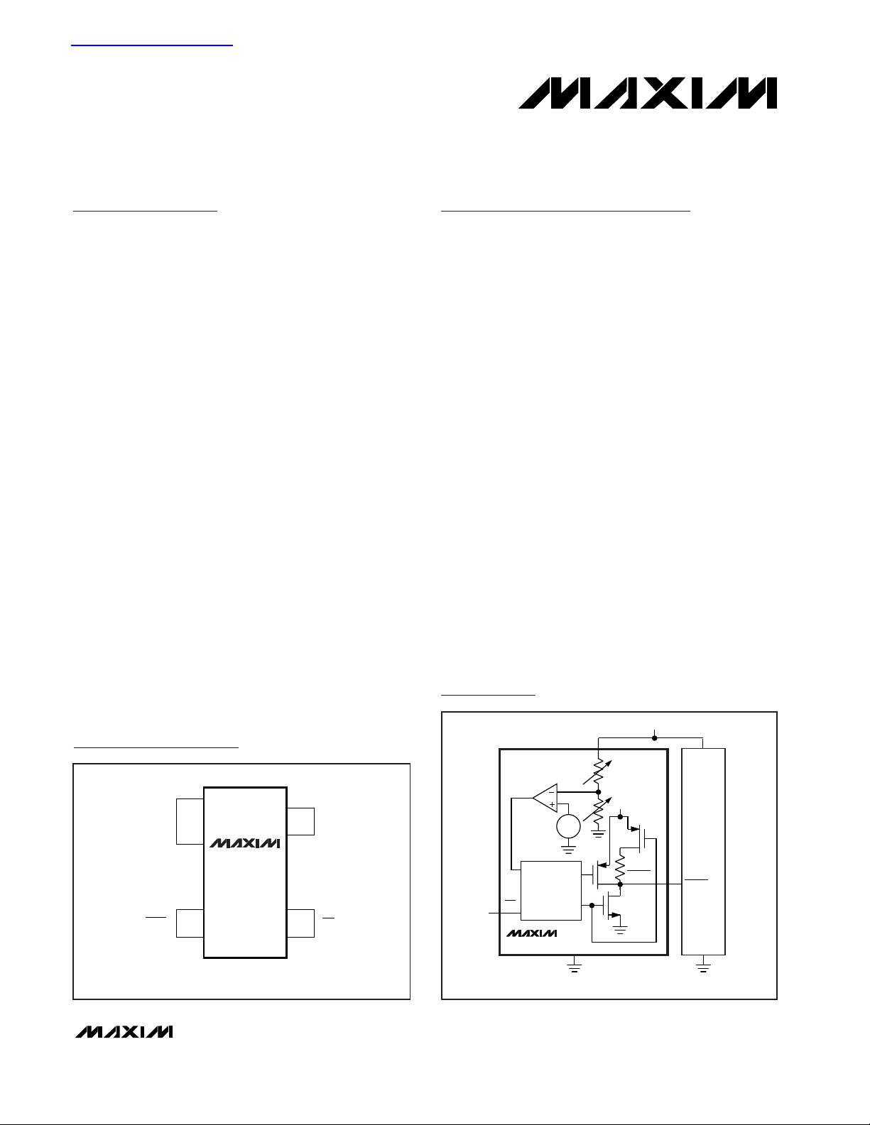
MAX6314*
68HC11/Bidirectional-Compatible
µP Reset Circuit
________________________________________________________________
Maxim Integrated Products
1
1
2
4
3
V
CC
MRRESET
GND
MAX6314
SOT143
TOP VIEW
Pin Configuration
MAX6314
V
CC
V
CC
GND
RESET
µP
RESET
MR
LASERTRIMMED
RESISTORS
V
CC
4.7k
68HC11**
**OR OTHER µC/µP WITH BIDIRECTIONAL RESET I/O PIN.
RESET
CIRCUITRY
Typical Operating Circuit
19-1090; Rev 1; 1/99
Ordering and Marking Information appears at end of
data sheet.
* Patents Pending
For free samples & the latest literature: http://www.maxim-ic.com, or phone 1-800-998-8800.
For small orders, phone 1-800-835-8769.
查询MAX6314*供应商
Page 2
V
MAX6314
68HC11/Bidirectional-Compatible
µP Reset Circuit
2 _______________________________________________________________________________________
ABSOLUTE MAXIMUM RATINGS
ELECTRICAL CHARACTERISTICS
(VCC= +2.5V to +5.5V, TA= -40°C to +85°C, unless otherwise noted. Typical values are at TA = +25°C.)
Stresses beyond those listed under “Absolute Maximum Ratings” may cause permanent damage to the device. These are stress ratings only, and functional
operation of the device at these or any other conditions beyond those indicated in the operational sections of the specifications is not implied. Exposure to
absolute maximum rating conditions for extended periods may affect device reliability.
Note 1: The MAX6314 monitors VCCthrough an internal, factory-trimmed voltage divider that programs the nominal reset threshold.
Factory-trimmed reset thresholds are available in 100mV increments from 2.5V to 5V (see
Ordering and Marking Information
).
Note 2: This is the minimum time RESET must be held low by an external pull-down source to set the active pull-up flip-flop.
Note 3: Measured from RESET V
OL
to (0.8 x VCC), R
LOAD
= ∞.
V
CC
........................................................................-0.3V to +6.0V
All Other Pins..............................................-0.3V to (V
CC
+ 0.3V)
Input Current (V
CC
).............................................................20mA
Output Current (RESET)......................................................20mA
Rate of Rise (V
CC
)...........................................................100V/µs
Continuous Power Dissipation (T
A
= +70°C)
SOT143 (derate 4mW/°C above +70°C).......................320mW
Operating Temperature Range ...........................-40°C to +85°C
Storage Temperature Range.............................-65°C to +160°C
Lead Temperature (soldering, 10sec).............................+300°C
T
A
= +25°C
VCC= 5.5V, no load
TA= 0°C to +70°C
VTH> 4.0V
VCC= falling at 1mV/µs
MAX6314US_ _D1-T
VCC> 4.25V, I
SINK
= 3.2mA
CONDITIONS
V
0.4
V
OL
RESET Output Voltage
kΩ32 63 100
MR Pull-Up Resistance
VTH- 1.8% V
THVTH
+ 1.8%
V
TH
Reset Threshold (Note 1)
µA
512
I
CC
V1.0 5.5V
CC
Operating Voltage Range
VCCSupply Current
ns500
MR to Reset Delay
ns100
MR Glitch Rejection
µs1
MR Minimum Input Pulse
V
0.8V
IL
MR Input Threshold
ppm/°C60∆VTH/°CReset Threshold Tempco
µs35VCCto Reset Delay
ms
1 1.4 2
t
RP
Reset Timeout Period
UNITSMIN TYP MAXSYMBOLPARAMETER
V
IL
V
IH
V
IH
VCC= 3.6V, no load
TA= -40°C to +85°C
VTH< 4.0V
MAX6314US_ _D3-T
MAX6314US_ _D2-T
MAX6314US_ _D4-T
VCC> 1.2V, I
SINK
= 0.5mA
VCC> 2.5V, I
SINK
= 1.2mA
VCC> 1.0V, I
SINK
= 80µA
410
VTH- 2.5% VTH+ 2.5%
1120 1570 2240
140 200 280
20 28 40
0.3 x V
CC
2.4
0.7 x V
CC
0.3
0.3
0.3
V
ns400t
S
Transition Flip-Flop Setup Time (Note 2)
VCC= 5V
VCC= 5V
mA20
RESET Active Pull-Up Current
V0.4 0.9Active Pull-Up Enable Threshold
VCC= 3V
ns
333
kΩ4.2 4.7 5.2
RESET Pull-Up Resistance
333
666
VCC= 5V
666
t
R
RESET Output Rise Time
(Note 3)
C
LOAD
= 120pF
C
LOAD
= 250pF
C
LOAD
= 200pF
C
LOAD
= 400pF
MANUAL RESET INPUT
RESET INTERNAL PULL-UP
Page 3
MAX6314
68HC11/Bidirectional-Compatible
µP Reset Circuit
_______________________________________________________________________________________ 3
__________________________________________Typical Operating Characteristics
(TA = +25°C, unless otherwise noted.)
4.7kΩ PULL-UP
2V/div
MAX6314 PULL-UP
2V/div
INPUT
5V/div
200ns/div
PULL-UP CHARACTERISTICS
MAX6314-01
100pF
4.7kΩ
+5V
74HC05
74HC05
V
CC
GND
MR
100pF
+5V
RESET
MAX6314
6
0
-50 -30 30 90
SUPPLY CURRENT vs. TEMPERATURE
2
1
5
MAX6314-02
TEMPERATURE (°C)
SUPPLY CURRENT (µA)
-10 10 50
3
4
70
VCC = 5V
VCC = 3V
VCC = 1V
6
0
0
1
35
SUPPLY CURRENT
vs. SUPPLY VOLTAGE
2
1
5
MAX6314-03
SUPPLY VOLTAGE (V)
SUPPLY CURRENT (µA)
2
3
4
4
TA = -40°C
TA = +25°C
TA = +85°C
50
0
-50 -30 10 90
POWER-DOWN RESET DELAY
vs. TEMPERATURE
10
40
MAX6314-04
TEMPERATURE (°C)
POWER-DOWN RESET DELAY (µs)
-10
20
30
30 50 70
VCC FALLING AT 1mV/µs
VTH = 4.63V
VTH = 3.00V
1.04
0.96
-50 -30 10 90
NORMALIZED RESET TIMEOUT PERIOD
vs. TEMPERATURE (V
CC
RISING)
0.97
0.98
1.02
1.00
1.03
MAX6314-05
TEMPERATURE (°C)
NORMALIZED RESET TIMEOUT PERIOD
-10
0.99
1.01
30 50 70
1.006
0.994
-50 -30 10 90
NORMALIZED RESET THRESHOLD
vs. TEMPERATURE (V
CC
FALLING)
0.996
0.998
1.004
1.000
MAX6314-06
TEMPERATURE (°C)
NORMALIZED RESET THRESHOLD
-10
1.002
30 50 70
100
0
10 100 1000
MAXIMUM TRANSIENT DURATION
vs. RESET COMPARATOR OVERDRIVE
20
MAX6314-07
RESET COMP. OVERDRIVE, VTH - VCC (mV)
MAXIMUM TRANSIENT DURATION (µs)
40
60
80
TA = +25°C
RESET OCCURS
ABOVE CURVE
VTH = 4.63V
VTH = 3.00V
600
0
-50 -30 10 90
RESET PULL-UP TIME
vs. TEMPERATURE
100
200
500
300
MAX6314-08
TEMPERATURE (°C)
RESET PULL-UP-TIME (ns)
-10
400
30 50 70
CL = 390pF
CL = 100pF
Page 4

Figure 1. Functional Diagram
MAX6314
68HC11/Bidirectional-Compatible
µP Reset Circuit
4 _______________________________________________________________________________________
______________________________________________________________Pin Description
Supply Voltage and Reset Threshold Monitor InputV
CC
4
Manual Reset Input. A logic low on MR asserts reset. Reset remains asserted as long as MR is low, and for
the reset timeout period (t
RP
) after the reset conditions are terminated. Connect to VCCif not used.
MR
3
PIN
Active-Low Complementary Output. In addition to the normal N-channel pull-down, RESET has a P-channel
pull-up transistor in parallel with a 4.7kΩ resistor to facilitate connection to µPs with bidirectional resets. See
the
Reset Output
section.
RESET
2
GroundGND1
FUNCTIONNAME
LASER-
TRIMMED
RESISTORS
V
CC
MAX6314
VREF
RESET
GENERATOR
2µs ONE-SHOT
V
CC
63k
MR
V
CC
TRANSITION
FLIP-FLOP
RQ
FF
S
ACTIVE PULL-UP
ENABLE COMPARATOR
0.5V
GND
4.7k
RESET
Page 5

MAX6314
68HC11/Bidirectional-Compatible
µP Reset Circuit
_______________________________________________________________________________________ 5
_______________Detailed Description
The MAX6314 has a reset output consisting of a 4.7kΩ
pull-up resistor in parallel with a P-channel transistor
and an N-channel pull down (Figure 1), allowing this IC
to directly interface with microprocessors (µPs) that
have bidirectional reset pins (see the
Reset Output
section).
Reset Output
A µP’s reset input starts the µP in a known state. The
MAX6314 asserts reset to prevent code-execution
errors during power-up, power-down, or brownout
conditions. RESET is guaranteed to be a logic low for
VCC> 1V (see the
Electrical Characteristics
). Once
VCCexceeds the reset threshold, the internal timer
keeps reset asserted for the reset timeout period (tRP);
after this interval RESET goes high. If a brownout condition occurs (monitored voltage dips below its programmed reset threshold), RESET goes low. Any time
VCCdips below the reset threshold, the internal timer
resets to zero and RESET goes low. The internal timer
starts when VCCreturns above the reset threshold, and
RESET remains low for the reset timeout period.
The MAX6314’s RESET output is designed to interface
with µPs that have bidirectional reset pins, such as the
Motorola 68HC11. Like an open-drain output, the
MAX6314 allows the µP or other devices to pull RESET
low and assert a reset condition. However, unlike a
standard open-drain output, it includes the commonly
specified 4.7kΩ pull-up resistor with a P-channel active
pull-up in parallel.
This configuration allows the MAX6314 to solve a problem associated with µPs that have bidirectional reset
pins in systems where several devices connect to
RESET. These µPs can often determine if a reset was
asserted by an external device (i.e., the supervisor IC)
or by the µP itself (due to a watchdog fault, clock error,
or other source), and then jump to a vector appropriate
for the source of the reset. However, if the µP does
assert reset, it does not retain the information, but must
determine the cause after the reset has occurred.
The following procedure describes how this is done
with the Motorola 68HC11. In all cases of reset, the µP
pulls RESET low for about four E-clock cycles. It then
releases RESET, waits for two E-clock cycles, then
checks RESET’s state. If RESET is still low, the µP concludes that the source of the reset was external and,
when RESET eventually reaches the high state, jumps
to the normal reset vector. In this case, stored state
information is erased and processing begins from
scratch. If, on the other hand, RESET is high after the
two E-clock cycle delay, the processor knows that it
caused the reset itself and can jump to a different vector and use stored state information to determine what
caused the reset.
The problem occurs with faster µPs; two E-clock cycles
is only 500ns at 4MHz. When there are several devices
on the reset line, the input capacitance and stray
capacitance can prevent RESET from reaching the
logic-high state (0.8 x V
CC
) in the allowed time if only a
passive pull-up resistor is used. In this case, all resets
will be interpreted as external. The µP is guaranteed to
sink only 1.6mA, so the rise time cannot be much
reduced by decreasing the recommended 4.7kΩ
pull-up resistance.
The MAX6314 solves this problem by including a pullup transistor in parallel with the recommended 4.7kΩ
resistor (Figure 1). The pull-up resistor holds the output
high until RESET is forced low by the µP reset I/O, or by
the MAX6314 itself. Once RESET goes below 0.5V, a
comparator sets the transition edge flip-flop, indicating
that the next transition for RESET will be low to high. As
soon as RESET is released, the 4.7kΩ resistor pulls
RESET up toward VCC. When RESET rises above 0.5V,
the active P-channel pull-up turns on for the 2µs
duration of the one-shot. The parallel combination of the
4.7kΩ pull-up and the P-channel transistor onresistance quickly charges stray capacitance on the
reset line, allowing RESET to transition low to high within the required two E-clock period, even with several
devices on the reset line (Figure 2). Once the one-shot
times out, the P-channel transistor turns off. This
process occurs regardless of whether the reset was
caused by VCCdipping below the reset threshold, MR
being asserted, or the µP or other device asserting
RESET. Because the MAX6314 includes the standard
4.7kΩ pull-up resistor, no external pull-up resistor is
required. To minimize current consumption, the internal
pull-up resistor is disconnected whenever the MAX6314
asserts RESET.
Manual Reset Input
Many µP-based products require manual reset capability, allowing the operator, a test technician, or external
logic circuitry to initiate a reset. A logic low on MR
asserts reset. Reset remains asserted while MR is low,
and for the reset active timeout period after MR returns
high. To minimize current consumption, the internal
4.7kΩ pull-up resistor on RESET is disconnected
whenever RESET is asserted.
Page 6
MAX6314
68HC11/Bidirectional-Compatible
µP Reset Circuit
6 _______________________________________________________________________________________
MR has an internal 63kΩ pull-up resistor, so it can be
left open if not used. Connect a normally open momentary switch from MR to GND to create a manual reset
function; external debounce circuitry is not required. If
MR is driven from long cables or if the device is used in
a noisy environment, connecting a 0.1µF capacitor from
MR to ground provides additional noise immunity.
__________Applications Information
Negative-Going VCCTransients
In addition to issuing a reset to the µP during power-up,
power-down, and brownout conditions, these devices
are relatively immune to short-duration negative-going
transients (glitches).
The Typical Operating Character-
istics
show the Maximum Transient Duration vs. Reset
Threshold Overdrive, for which reset pulses are not
generated. The graph was produced using negativegoing pulses, starting at V
RST
max and ending below
the programmed reset threshold by the magnitude
indicated (reset threshold overdrive). The graph shows
the maximum pulse width that a negative-going V
CC
transient may typically have without causing a reset
pulse to be issued. As the amplitude of the transient
increases (i.e., goes farther below the reset threshold),
the maximum allowable pulse width decreases. A 0.1µF
bypass capacitor mounted close to VCCprovides additional transient immunity.
Ensuring a Valid
RESET
Output
Down to V
CC
= 0V
When VCCfalls below 1V, RESET no longer sinks
current—it becomes an open circuit. Therefore, highimpedance CMOS-logic inputs connected to RESET
can drift to undetermined voltages. This presents no
problem in most applications, since most µP and other
circuitry is inoperative with VCCbelow 1V. However, in
applications where RESET must be valid down to
V
CC
= 0V, adding a pull-down resistor to RESET will
cause any stray leakage currents to flow to ground,
holding RESET low (Figure 3). R1’s value is not critical;
100kΩ is large enough not to load RESET and small
enough to pull RESET to ground.
Figure 2. MAX6314 Supports Additional Devices on the Reset Bus
4.7k
MR
C
IN
RESET
RESET
CIRCUITRY
V
CC
MAX6314
C
STRAY
68HC11
RESET
CIRCUITRY
C
IN
RESET
V
CC
OTHER DEVICES
C
IN
RESET
Figure 3. RESET Valid to VCC= Ground Circuit
MAX6314
V
CC
GND
RESET
R1
Page 7

MAX6314
68HC11/Bidirectional-Compatible
µP Reset Circuit
_______________________________________________________________________________________ 7
Figure 4. RESET Timing Diagram
t
R
t
S
RESET
RESET PULLED LOW
BY µC OR
RESET GENERATOR
ACTIVE
PULL-UP
TURNS ON
V
CC
0.5V
0.8 x V
CC
t
RP
OR
µC RESET DELAY
†
The MAX6314 is available in a SOT143 package, -40°C to +85°C temperature range.
††
The first two letters in the package top mark identify the part, while the remaining two letters are the lot tracking code.
†††
Sample stocks generally held on the bolded products; also, the bolded products have 2,500 piece minimum-order quantities.
Non-bolded products have 10,000 piece minimum-order quantities. Contact factory for details.
Note: All devices available in tape-and-reel only. Contact factory for availability.
__________________________________________Ordering and Marking Information
PART
†
MAX6314US46D1-T 4.63 1 AE_ _
MAX6314US49D1-T 4.90
NOMINAL
VTH(V)
MIN t
RP
(ms)
1 AB_ _
MAX6314US47D1-T 4.70 1 AD_ _
PKG. TOP
MARK
††
MAX6314US48D1-T 4.80 1 AC_ _
MAX6314US50D1-T 5.00 1 AA_ _
MAX6314US45D1-T 4.50 1 AF_ _
MAX6314US44D1-T
†††
4.39 1 AG_ _
MAX6314US43D1-T 4.30 1 AH_ _
MAX6314US42D1-T 4.20 1 AI_ _
MAX6314US41D1-T 4.10 1 AJ_ _
MAX6314US40D1-T 4.00 1 AK_ _
MAX6314US39D1-T 3.90 1 AL_ _
MAX6314US38D1-T 3.80 1 CA_ _
MAX6314US37D1-T 3.70 1 CB_ _
MAX6314US36D1-T 3.60 1 CC_ _
MAX6314US35D1-T 3.50 1 CD_ _
MAX6314US34D1-T 3.40 1 CE_ _
MAX6314US33D1-T 3.30 1 CF_ _
MAX6314US32D1-T 3.20 1 CG_ _
MAX6314US31D1-T 3.08 1 CH_ _
MAX6314US30D1-T 3.00 1 CI_ _
MAX6314US29D1-T 2.93 1 CJ_ _
PART
†
MAX6314US37D2-T 3.70 20 DB_ _
MAX6314US36D2-T 3.60
NOMINAL
VTH(V)
MIN t
RP
(ms)
20 DC_ _
MAX6314US34D2-T 3.40 20 DE_ _
PKG. TOP
MARK
††
MAX6314US33D2-T 3.30 20 DJ_ _
MAX6314US35D2-T 3.50 20 DD_ _
MAX6314US26D1-T
†††
2.63 1 CM_ _
MAX6314US27D1-T 2.70 1 CL_ _
MAX6314US28D1-T 2.80 1 CK_ _
MAX6314US25D1-T 2.50 1 CN_ _
MAX6314US50D2-T 5.00 20 CO_ _
MAX6314US49D2-T 4.90 20 CP_ _
MAX6314US48D2-T 4.80 20 CQ_ _
MAX6314US47D2-T 4.70 20 CR_ _
MAX6314US46D2-T 4.63 20 CS_ _
MAX6314US45D2-T 4.50 20 CT_ _
MAX6314US44D2-T
†††
4.39 20 CU_ _
MAX6314US43D2-T 4.30 20 CV_ _
MAX6314US42D2-T 4.20 20 CW_ _
MAX6314US41D2-T 4.10 20 CX_ _
MAX6314US40D2-T 4.00 20 CY_ _
MAX6314US39D2-T 3.90 20 CZ_ _
MAX6314US38D2-T 3.80 20 DA_ _
Page 8

MAX6314
68HC11/Bidirectional-Compatible
µP Reset Circuit
Maxim cannot assume responsibility for use of any circuitry other than circuitry entirely embodied in a Maxim product. No circuit patent licenses are
implied. Maxim reserves the right to change the circuitry and specifications without notice at any time.
8
_____________________Maxim Integrated Products, 120 San Gabriel Drive, Sunnyvale, CA 94086 408-737-7600
© 1999 Maxim Integrated Products Printed USA is a registered trademark of Maxim Integrated Products.
_____________________________Ordering and Marking Information (continued)
†
The MAX6314 is available in a SOT143 package, -40°C to +85°C temperature range.
††
The first two letters in the package top mark identify the part, while the remaining two letters are the lot tracking code.
†††
Sample stocks generally held on the bolded products; also, the bolded products have 2,500 piece minimum-order quantities.
Non-bolded products have 10,000 piece minimum-order quantities. Contact factory for details.
Note: All devices available in tape-and-reel only. Contact factory for availability.
Chip Information
TRANSISTOR COUNT: 519
PART
†
NOMINAL
VTH(V)
MIN t
RP
(ms)
PKG. TOP
MARK
††
MAX6314US32D2-T 3.20 20 DK_ _
MAX6314US31D2-T 3.08 20 DL_ _
MAX6314US30D2-T 3.00 20 DM_ _
MAX6314US29D2-T 2.93 20 DN_ _
MAX6314US28D2-T 2.80 20 DO_ _
MAX6314US27D2-T 2.70 20 DP_ _
MAX6314US26D2-T
†††
2.63 20 DQ_ _
MAX6314US25D2-T 2.50 20 DR_ _
MAX6314US50D3-T 5.00 140 DS_ _
MAX6314US49D3-T 4.90 140 DT_ _
MAX6314US48D3-T 4.80 140 DU_ _
MAX6314US47D3-T 4.70 140 DV_ _
MAX6314US46D3-T
†††
4.63 140 DW_ _
MAX6314US45D3-T 4.50 140 DX_ _
MAX6314US44D3-T
†††
4.39 140 DY_ _
MAX6314US43D3-T 4.30 140 DZ_ _
MAX6314US42D3-T 4.20 140 EA_ _
MAX6314US41D3-T 4.10 140 EB_ _
MAX6314US40D3-T 4.00 140 EC_ _
MAX6314US39D3-T 3.90 140 EG_ _
MAX6314US38D3-T 3.80 140 EH_ _
MAX6314US37D3-T 3.70 140 EI_ _
MAX6314US36D3-T 3.60 140 EJ_ _
MAX6314US35D3-T 3.50 140 EK_ _
MAX6314US34D3-T 3.40 140 EL_ _
MAX6314US33D3-T 3.30 140 EM_ _
MAX6314US32D3-T 3.20 140 EN_ _
MAX6314US31D3-T
†††
3.08 140 EO_ _
MAX6314US30D3-T 3.00 140 EP_ _
MAX6314US29D3-T
†††
2.93 140 ES_ _
FW_ _11202.50MAX6314US25D4-T
FV_ _11202.63
MAX6314US26D4-T
†††
FU_ _11202.70MAX6314US27D4-T
FT_ _11202.80MAX6314US28D4-T
FS_ _11202.93MAX6314US29D4-T
FR_ _11203.00MAX6314US30D4-T
FQ_ _11203.08MAX6314US31D4-T
FP_ _11203.20MAX6314US32D4-T
FO_ _11203.30MAX6314US33D4-T
FN_ _11203.40MAX6314US34D4-T
FM_ _11203.50MAX6314US35D4-T
FL_ _11203.60MAX6314US36D4-T
FK_ _11203.70MAX6314US37D4-T
FJ_ _11203.80MAX6314US38D4-T
FI_ _11203.90MAX6314US39D4-T
FH_ _11204.00MAX6314US40D4-T
FG_ _11204.10MAX6314US41D4-T
FF_ _11204.20MAX6314US42D4-T
FE_ _11204.30MAX6314US43D4-T
FD_ _11204.39
MAX6314US44D4-T
†††
FC_ _11204.50MAX6314US45D4-T
FB_ _11204.63MAX6314US46D4-T
EW_ _1402.50MAX6314US25D3-T
PKG. TOP
MARK
††
ET_ _
EU_ _
EV_ _140
140
140
MIN t
RP
(ms)
NOMINAL
VTH(V)
2.80
2.70
2.63
MAX6314US26D3-T
†††
MAX6314US27D3-T
MAX6314US28D3-T
PART
†
FA_ _11204.70MAX6314US47D4-T
EX_ _
EY_ _
EZ_ _1120
1120
11205.00
4.90
4.80MAX6314US48D4-T
MAX6314US49D4-T
MAX6314US50D4-T
 Loading...