

19-0329; Rev 0; 12/94
EVALUATION KIT MANUAL
FOLLOWS DATA SHEET
High-Accuracy, Low-Dropout
Linear Regulators
_______________General Description
The MAX687/MAX688/MAX689 low-dropout linear regulators operate with an input-to-output voltage differential limited only by an external PNP transistor. Outputs are fixed
at 3.3V (MAX687/MAX688) or 3.0V (MAX689). The only
external components required are a PNP pass transistor
and output, compensation, and bypass capacitors. Base
drive to the external transistor is at least 10mA, permitting
output currents to exceed 1A when using high-gain transistors (β > 100). Output current limiting is implemented
by limiting the external transistor’s base current. Output
voltage monitoring and shutdown functions are included.
The 3.3V MAX687 automatically shuts down whenever
the output voltage drops below 2.96V. An internal
power-fail comparator also monitors the output and provides an early warning of low output voltage before the
device shuts down. When shut down, the output is
latched off until the ON input is pulsed. Turning off the
power supply in this way prevents battery damage due
to excessive discharge or cell-reversal. Typical applications include portable telephones and other battery-powered equipment where the power supply must be
disabled when the battery voltage is low.
The MAX688 and MAX689 do not have an automatic
shutdown function, and are identical except for their
output voltages. Each device has an active-low shutdown-control input, used to turn its output on or off at
any time. As SHDN falls, the device enters a standby
mode before fully shutting down. When in standby, the
reference and comparators are fully operational, permitting the transition from normal mode to standby
mode to occur at a precise voltage level on SHDN.
________________________Applications
High-Efficiency Linear Regulator
Battery-Powered Devices
Portable Instruments
Portable Telephones
Power Supply or Backup Supply for Memory
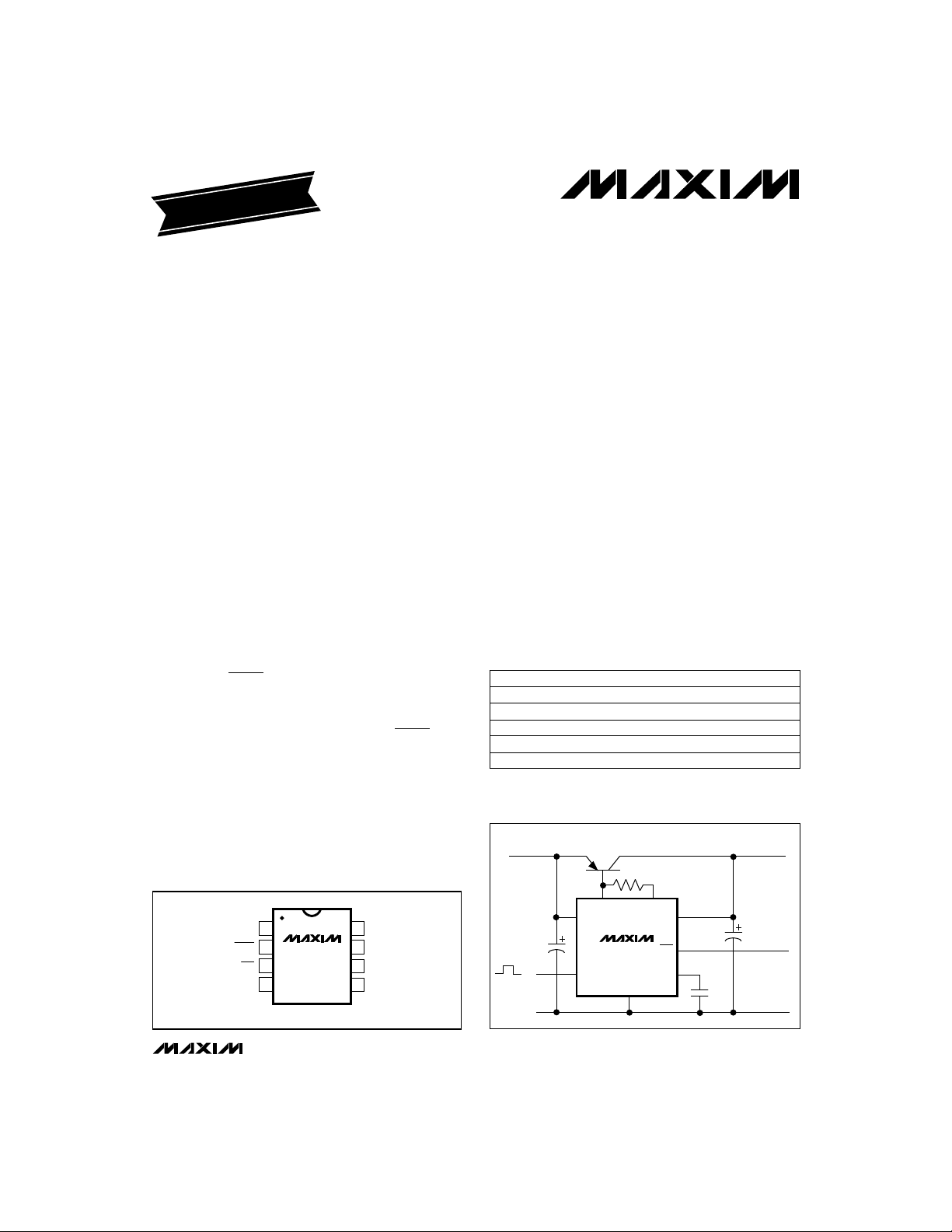
__________________Pin Configuration
____________________________Features
♦ Fixed Outputs:
3.3V (MAX687/MAX688)
3.0V (MAX689)
♦ Directly Drives External PNP Transistor
♦ 10mA Min Base-Current Drive for >1A Output
♦ Low Dropout Voltage:
100mV Dropout at 650mA Output (FZT749)
40mV Dropout at 200mA Output (FZT749)
0.8V Dropout at 4A Output
♦ Power-Fail Output Monitors the Output Voltage
♦ Automatic, Latched Shutdown when Output Falls Out
of Regulation (MAX687)
♦ Precision Threshold Shutdown Control
(MAX688/MAX689)
♦ Low Supply Current:
150µA Operating
<1µA Shutdown
♦ 2.7V to 11.0V Supply Range
♦ 8-Pin DIP/SO/µMAX Packages
♦ <2mV Line Transient with 3.4V to 3.6V Input
♦ Output Accuracy <±2%
______________Ordering Information
PART
MAX687CPA
MAX687CSA
MAX687CUA 0°C to +70°C
MAX687EPA
MAX687ESA -40°C to +85°C
Ordering Information continued at end of data sheet.
TEMP. RANGE PIN-PACKAGE
0°C to +70°C
0°C to +70°C
-40°C to +85°C 8 Plastic DIP
8 Plastic DIP
8 SO
8 µMAX
8 SO
__________Typical Operating Circuit
+3.5V to +5V INPUT
Q1
FZT749
12Ω
R
B
3.3V @ 500mA
MAX687/MAX688/MAX689
TOP VIEW
(ON) SHDN
( ) ARE FOR MAX687
IN
1
2
MAX687
MAX688
3
PFO
GND
MAX689
4
DIP/SO/µMAX
________________________________________________________________
CC
8
BASE
7
BLIM
6
OUT
5
2.2µF
ON
C1
GND
BASE
IN
ON
BLIM
MAX687
GND
Maxim Integrated Products
Call toll free 1-800-998-8800 for free samples or literature.
OUT
PFO
C2
68µF
POWER-FAIL
OUTPUT
CC
C3
10nF
1
High-Accuracy, Low-Dropout
Linear Regulators
ABSOLUTE MAXIMUM RATINGS
Input Supply Voltage IN to GND............................................12V
Terminal Voltages to GND
(MAX687)........................................-0.3V to V
PFO
(MAX688/MAX689) ......................................-0.3V to 12V
PFO
All Remaining Pins .....................................-0.3V to V
Sink Current ...............................................................10mA
PFO
Source Current (MAX687)...........................................10mA
PFO
Stresses beyond those listed under “Absolute Maximum Ratings” may cause permanent damage to the device. These are stress ratings only, and functional
operation of the device at these or any other conditions beyond those indicated in the operational sections of the specifications is not implied. Exposure to
absolute maximum rating conditions for extended periods may affect device reliability.
OUT
IN
+ 0.3V
+ 0.3V
Continuous Power Dissipation (T
Plastic DIP (derate 9.09mW/°C above +70°C) ............727mW
SO (derate 5.88mW/°C above +70°C).........................471mW
µMAX (derate 4.1mW/°C above +70°C) ......................330mW
Operating Temperature Ranges
MAX68_C_A .......................................................0°C to +70°C
MAX68_E_A ....................................................-40°C to +85°C
Storage Temperature Range.............................-65°C to +165°C
Lead Temperature (soldering, 10sec).............................+300°C
ELECTRICAL CHARACTERISTICS
(VIN= 3.8V, SHDN = VIN(MAX688/MAX689), RB= 0Ω, C1 = 2.2µF, C2 = 10µF, C3 = 10nF, TA= T
noted. Typical values are at T
LINEAR REGULATOR
Supply Voltage
MAX687/MAX688/MAX689
Output Voltage
Dropout Voltage (Note 2)
Line Regulation
Supply Current
BASE Sink Current
Base-Current Limit
= +25°C.)
A
V
OUT
I
GND
BASE
CONDITIONS
(Note 1)
IN
MAX687/MAX688
MAX689
PNP = FZT749, I
OUT
MAX687/MAX688
MAX689
1µA ≤ I
VIN= 3.8V,
PNP = FZT749,
no load
V
BASE
RBis connected from BASE to BLIM (Ω),
RB= 0Ω to 100Ω
(Note 3)
PNP = FZT749, I
≤ 10mA
BASE
= VIN- 1V
= 200mA, C2 = 20µF
LOAD
= 100mA (Note 4)
LOAD
VIN= 3.8V, I
3.8V ≤ VIN≤ 11.0V,
1µA ≤ I
VIN= 3.5V, I
3.5V ≤ VIN≤ 11.0V,
1µA ≤ I
3.8V ≤ VIN≤ 11.0V,
I
= 1mA
BASE
3.5V ≤ VIN≤ 11.0V,
I
= 1mA
BASE
On
Standby,
MAX688/MAX689
Shutdown
BASE
BASE
BASE
≤ 10mA
BASE
≤ 10mA
= 1mA
= 1mA
= +70°C)
A
to T
MIN
3.2 3.3 3.4
3.13 3.3 3.47
2.9 3.0 3.1
2.85 3.0 3.15
70 100 130
+ 5Ω RB+ 5Ω RB+ 5Ω
R
B
, unless otherwise
MAX
0.4 1.4
0.4 1.4
150 250
11 25
< 0.02 1
UNITSMIN TYP MAXSYMBOLPARAMETER
V2.7 11.0V
V
mV40VIN- V
mV/V
mV45 60Load Regulation
µA
mA10 20 40I
mA
µs300Start-Up Time
%2Start-Up Overshoot
µF10C2Load Capacitance
2 _______________________________________________________________________________________
High-Accuracy, Low-Dropout
Linear Regulators
ELECTRICAL CHARACTERISTICS (continued)
(VIN= 3.8V, SHDN = VIN(MAX688/MAX689), RB= 0Ω, C1 = 2.2µF, C2 = 10µF, C3 = 10nF, TA= T
noted. Typical values are at T
= +25°C.)
A
CONDITIONS
MAX687: ON, PFO, SHDN
V
PFT
NOM
V
PFT
SD
OH
OL
-
- V
SD
IH
IL
Falling V
Falling V
Falling V
I
SOURCE
I
SINK
, comparators monitor V
OUT
, comparators monitor V
OUT
, comparators monitor V
OUT
= 50µA, part on, VIN= 2.7V VV
= 1.2mA, VIN= 2.7V V0.06 0.3V
Output turns on
Output remains off 0.2V
OUT
OUT
OUT
PFO Threshold Voltage Below
V
(Note 5)
NOM
Shutdown Threshold Voltage
Below V
PFT
Shutdown Threshold Voltage
PFO Output Voltage High
PFO Output Voltage Low
ON Threshold Voltage
MAX688/MAX689: SHDN, PFO
PFO Threshold Voltage
SHDN Threshold Voltages
V
PFT
SON
SSY
SSD
Falling V
parators monitor V
OUT
, com-
On, SHDN falling
Standby
Shutdown
MAX688
OUT
MAX689 2.77 2.85 2.89
Rising SHDN, standby→on
V
= 1.23V nA-25 25SHDN Input Current
SHDN
Glitch immunity
I
PFO Output Voltage Low
OL
PFO Off Leakage Current
Output Noise Voltage
Note 1: Minimum VINfor regulated V
ence and comparators are functional down to the minimum voltage specified, but the output may not be in regulation.
Note 2: Dropout voltage is defined as V
Note 3: The start-up time specification is the time taken from ON or SHDN
e
n
depends on the characteristics of the external PNP transistor, and on the load. The refer-
OUT
- V
IN
and is a function of load capacitance, C2, and load resistance, R
Note 4: Minimum load capacitance is a function of RL. Minimum C2 = 10µF for loads up to 100mA and 1µF/10mA for higher loads.
ESR of C2 should be no larger than 1/100 of R
Note 5: The nominal output voltage, V
, is defined under the default conditions of testing: VIN= 3.8V, I
NOM
= 1.2mA, VIN= 2.7V
SINK
V
= 11V, V
PFO
10Hz ≤ f ≤ 10kHz, I
10Hz ≤ f ≤ 1MHz, I
when V
OUT
OUT
. Guaranteed by design.
L
> 1.25V
SHDN
= 200mA
LOAD
= 200mA
LOAD
is 50mV below its value at VIN= V
rising to BASE sinking current. V
.
L
NOM
to T
, unless otherwise
MAX
OUT
MIN
- 0.3V
1.0V
3.07 3.13 3.19
1.25V
1.0 1.2V
0.2V
66
105
+ 1V.
rise time is longer
OUT
= 1mA, TA= T
BASE
MIN
UNITSMIN TYP MAXSYMBOLPARAMETER
µV
to T
MAX687/MAX688/MAX689
mV110 170
mV7PFO Hysteresis
mV20 70V
V2.96V
V
nA0.2 100ON Input Leakage Current
V
mV7PFO Hysteresis
V
mV70SHDN Hysteresis
µs100PFO, SHDN Transient Rejection
V0.06 0.3V
µA1
RMS
.
MAX
_______________________________________________________________________________________ 3
High-Accuracy, Low-Dropout
Linear Regulators
__________________________________________Typical Operating Characteristics
(Circuits of Figures 1 and 2, VIN= 5V, Q1 = FZT749, TA = +25°C, unless otherwise noted.)
MAX689
50 100 250200150
NUMBER OF UNITS
OUTPUT VOLTAGE DISTRIBUTION
3.32289
3.31932
3.31576
3.31219
3.30862
3.30505
3.30149
3.29792
OUTPUT VOLTAGE (V)
3.29435
3.29078
3.28722
3.28365
0 50 100 250200150
MAX687
NUMBER OF UNITS
3.32145
3.31920
3.31696
MAX687/9-02
3.31472
3.31248
3.31024
3.30800
3.30576
3.30352
3.30128
3.29904
OUTPUT VOLTAGE (V)
3.29679
3.29455
3.29231
3.29007
3.28783
OUTPUT VOLTAGE DISTRIBUTION
MAX688
0 50 100
NUMBER OF UNITS
MAX687/9-01
250200150
OUTPUT VOLTAGE DISTRIBUTION
3.01595
3.01420
3.01245
3.01071
3.00896
3.00721
3.00547
3.00372
3.00198
3.00023
OUTPUT VOLTAGE (V)
2.99848
2.99674
2.99499
2.99324
2.99150
2.98975
0
MAX687/9-03
DROPOUT VOLTAGE
0.30
vs. LOAD CURRENT
Q1 = FZT749
RB = 0Ω
0.25
MAX687/MAX688/MAX689
0.20
(V)
OUT
0.15
- V
IN
V
0.10
0.05
0
0 200 600 1000 1400 1800
OBSERVE MAXIMUM POWER
DISSIPATION LIMIT OF
EXTERNAL PASS TRANSISTOR.
MAX687/9-05
1.0
0.9
0.8
0.7
(V)
0.6
OUT
0.5
- V
IN
0.4
V
0.3
0.2
0.1
0
LOAD CURRENT (mA)
GND CURRENT vs. DROPOUT VOLTAGE
7
6
5
4
3
GND CURRENT (mA)
2
1
0
0 0.1 0.2 0.3 0.4 0.5 0.6 0.7 0.8 0.9 1.0
300mA LOAD
100mA LOAD
VIN - V
OUT
10mA LOAD
(V)
MAX687/9-7
GND CURRENT (mA)
7
6
5
4
3
2
1
0
DROPOUT VOLTAGE
vs. LOAD CURRENT
Q1 = 2N2907
RB = 0Ω
0 200 600 1000
400 800
LOAD CURRENT (mA)
GND CURRENT vs. DROPOUT VOLTAGE
300mA LOAD
100mA LOAD
0812345 76
VIN - V
OUT
10mA LOAD
(V)
GND CURRENT
vs. LOAD CURRENT
6
MAX687/9-5
5
4
3
GND CURRENT (mA)
2
1
0
0 200 400 600 800 1000 1200
LOAD CURRENT (mA)
NO-LOAD SUPPLY CURRENT
vs. TEMPERATURE
146
144
MAX687/9-8
142
140
138
136
134
132
SUPPLY CURRENT (µA)
130
128
126
-55 -25 0 25 50 75 100 125
TEMPERATURE (°C)
MAX687/9-06
MAX687/9-9
4 _______________________________________________________________________________________

High-Accuracy, Low-Dropout
Linear Regulators
____________________________Typical Operating Characteristics (continued)
(Circuits of Figures 1 and 2, VIN= 5V, Q1 = FZT749, TA = +25°C, unless otherwise noted.)
SHUTDOWN SUPPLY CURRENT
vs. TEMPERATURE
-55 -25 0 25 50 75 100 125
TEMPERATURE (°C)
SHUTDOWN SUPPLY CURRENT (µA)
0.3000
0.2500
0.2000
0.1500
0.1000
0.0500
0
LINE-TRANSIENT RESPONSE
I
= 70mA
LOAD
C1 = 2.2µF
C2 = 20µF
C3 = 10nF
2ms/div
LOAD-TRANSIENT RESPONSE
V
OUT
3.3V
1mV/div
V
IN
3.6V
V
IN
3.4V
3.315
MAX687/9-10
3.310
3.305
3.300
3.295
OUTPUT VOLTAGE (V)
3.290
3.285
3.280
-55 -25 0 25 50 75 100 125
I
= 200mA
LOAD
C1 = 2.2µF
C2 = 20µF
C3 = 10nF
OUTPUT VOLTAGE
vs. TEMPERATURE
TEMPERATURE (°C)
LINE-TRANSIENT RESPONSE
2ms/div
RIPPLE REJECTION vs. FREQUENCY
80
70
MAX687/9-11
60
= 3.6V Min
V
50
IN
I
= 200mA
LOAD
40
30
RIPPLE REJECTION (dB)
20
10
C2 = 20µF
0
10 100 1k 10k 100k
POWER-UP AND EXIT FROM SHUTDOWN
V
OUT
3.3V
1mV/div
V
IN
3.6V
V
IN
3.4V
I
= 500mA
LOAD
C1 = 2.2µF
C2 = 68µF
C3 = 10nF
LOAD-TRANSIENT RESPONSE
MAX687/MAX688
V
= 4.3V Min
IN
I
= 20mA
LOAD
FREQUENCY (Hz)
MAX687/MAX688
1ms/div
MAX687/MAX688/MAX689
MAX687/9-16
V
IN
5V/div
V
OUT
1V/div
SHDN
5V/div
V
OUT
3.3V
10mV/div
500mA
I
LOAD
200mA/div
0mA
VIN = 3.4V
100µs/div
= 3.5V
V
IN
100µs/div
_______________________________________________________________________________________
V
OUT
3.3V
10mV/div
500mA
I
LOAD
200mA/div
0mA
5

High-Accuracy, Low-Dropout
Linear Regulators
______________________________________________________________Pin Description
NAME FUNCTION
PIN
1 IN Positive input voltage, 2.7V to 11.0V
ON
(MAX687)
2
SHDN
2
(MAX688/
MAX689)
3 PFO
4 GND Ground
5 OUT Regulator Output. MAX687/MAX688, 3.3V; MAX689, 3.0V.
6 BLIM
MAX687/MAX688/MAX689
7 BASE
8 CC Compensation Capacitor. Connect a non-polarized capacitor (10nF to 100nF) from CC to GND.
ON activates the regulator when pulsed high. In order for the regulator to remain on, ON must remain high
until V
and remains latched off until ON is pulsed high. When powered up, the MAX687 does not start up until ON
is pulsed high. Connect to VINif not used.
SHDN is a three-level input that controls the mode of operation. The device is on when V
The output is disabled and the supply current is reduced (IIN< 25µA, standby mode) when V
and is fully off (IIN< 1µA, shutdown mode) when V
tion is not used. PFO is low when SHDN is low (below 0.2V).
Power-Fail Output. PFO trips when V
sinks current in the MAX687, but is an open drain in the MAX688/MAX689. When shut down, PFO is always
low and sinks current. Leave PFO open if not used.
Base current limit. A resistor (RB) connected between BASE and BLIM sets the maximum base drive to the
PNP transistor: I
vides current limiting without using a current-sense resistor in the collector of the external PNP, thus not
impacting dropout. Output current limiting accuracy depends on how well the external PNP beta (hFE) is
controlled. Connect to BASE if not used.
Base drive for the external PNP transistor. Current limiting is controlled using a resistor (RB) connected
between BASE and BLIM. For maximum output current, connect BASE to BLIM.
exceeds the internal shutdown threshold voltage. The MAX687 is shut down when V
OUT
< 0.2V. Connect SHDN to IN if the shutdown func-
SHDN
is 170mV below nominal V
OUT
≤ 0.1V / (RB + 5Ω). This limits quiescent current rise during dropout and also pro-
BASE
OUT
at I
= 1mA. PFO sources and
BASE
SHDN
OUT
> 1.25V.
SHDN
< 2.96V,
< 1.2V,
_______________Detailed Description
The MAX687/MAX688/MAX689 are precision lowdropout linear regulators employing external PNP transistors to achieve a wide range of output currents at
voltages of 3.0V or 3.3V. The maximum base current
for the PNP can be limited using a resistor. Limiting the
base drive keeps high currents from being wasted
when the device is in dropout (e.g., at low input voltages), and limits the regulator’s output current. The
dropout voltage is limited only by the PNP transistor’s
V
the output voltage drops 170mV below the nominal
level.
The three devices differ in their output voltages, in their
shutdown-control functions, and in PFO’s output drive
(see Table 1).
6 _______________________________________________________________________________________
. The Power-Fail Output (PFO) goes low when
CE(SAT)
Table 1. Device Functions
FUNCTION MAX687 MAX688 MAX689
V
OUT
Shutdown
Control
PFO Sources & Sinks Open Drain Open Drain
The MAX687’s output voltage is internally monitored; a
falling V
OUT
put falls further, the MAX687 automatically enters a lowpower shutdown mode, where the base drive to the
external PNP is cut off. PFO trips at a minimum of
110mV below the nominal V
by 2.96V. PFO is guaranteed to trip before the device
3.3V 3.3V 3.0V
Automatic at low
V
. Latched.
OUT
Use ON to start.
External
SHDN
is signaled by PFO going low. As the out-
, and shutdown occurs
OUT
External
SHDN

High-Accuracy, Low-Dropout
Linear Regulators
shuts down. Once the MAX687 is shut down, it can
only be turned on again when (a) the ON pin is pulsed
high, and (b) the conditions that triggered shutdown
have changed (e.g., the load has been reduced or the
input voltage has increased). In order for the MAX687
to latch into its on state, the ON pulse must remain high
until the output voltage has risen above the shutdown
threshold. The internal shutdown can be used to prevent deep discharge of a battery, for example, to provide “self backup” of CMOS RAM or to protect the
battery itself.
The RC circuit attached to the ON input in Figure 1
achieves automatic start-up at power-on by delivering a
brief pulse whenever the input voltage is suddenly
applied. This circuit is not suitable for applications
where the input voltage rises slowly. The RC values
should be chosen to keep ON high until the output rises
above about 3.13V. The values shown in Figure 1 for
C4 and R1 (0.1µF and 10kΩ) are suitable for most
applications. To ensure start-up when the input voltage
is very close to the circuit’s dropout voltage, when the
circuit is used to drive a very large capacitive load, or
for high-power circuits (I
> 3A), increase the value
LOAD
of R1 to increase the ON pulse width.
The 3.3V MAX688 and the 3.0V MAX689 incorporate
the same PFO warning whenever V
OUT
droops.
However, the MAX688/MAX689 do not automatically
shut down when the output voltage drops even further.
Instead, the SHDN input controls external shutdown.
As SHDN is pulled low, the chip first enters a low-current standby state (<25µA). The threshold at which
standby mode is entered is precisely controlled (±2%)
so the output can be turned off at a well-defined point.
70mV of hysteresis between the standby and on states
prevents chatter between the two modes. The voltage
applied to the SHDN pin can be derived from a resistive divider from VIN. When V
is less than 1.2V,
SHDN
the output is off. The device is fully shut down (<1µA)
when SHDN is pulled below 200mV. SHDN is not
latched, and as SHDN is raised, the MAX688/MAX689
exit shutdown and enter the standby mode. At the
higher SHDN threshold, the output is turned on.
Figure 1 shows a typical circuit for the MAX687, and
Figure 2 shows the same circuit configured for the
MAX688/MAX689.
The accuracy of the output current limit depends on
accurate knowledge of the PNP pass transistor’s current gain (hFE). With RB= 12Ω, BLIM limits base current to 6mA (I
Current Limiting
= 0.1V / (RB+ 5Ω)). See
BASE
section.
Base-
The PFO comparators on all three devices, and the internal
shutdown comparator on the MAX687, reject high-speed
spikes (<100µs). This reduces the PFOoutput’s noise sensitivity, and stops the MAX687 from being shut down inadvertently when there is noise on the input supply.
_______________Transistor Selection
The PNP pass transistor must meet specifications for
• current gain,
• power dissipation, and
• collector current.
The hFEinfluences the maximum output current the circuit can deliver. The largest guaranteed output current
Specifications
MAX687/MAX688/MAX689
+5V INPUT
C4
0.1µF
2.2µF
GND
ON CAN BE DRIVEN DIRECTLY FROM LOGIC WHEN R1 AND C4 ARE NOT USED.
Figure 1. MAX687 Operating Circuit
Q1 FZT749
12Ω
R
B
MAX687
GND
BLIM
OUT
PFO
CC
BASE
IN
C1
ON
R1
10kΩ
_______________________________________________________________________________________ 7
68µF
C2
C3
10nF
3.3V @ 500mA
POWER FAIL
12Ω
3.3V/ 3.0V @ 500mA
BLIM
OUT
PFO
CC
C3
10nF
+5V INPUT
2.2µF
ON / OFF
GND
Figure 2. MAX688/MAX689 Operating Circuit
Q1 FZT749
R
B
BASE
IN
C1
SHDN
MAX688
MAX689
GND
C2
68µF
POWER FAIL
R2
100k

High-Accuracy, Low-Dropout
Linear Regulators
is given by I
sistor’s rated power dissipation must exceed the actual
power dissipated in the transistor. The power dissipated (PD) equals the maximum load current (I
times the maximum input to output voltage differential:
PD = I
sistor collector current must exceed the maximum load
current. Suitable transistors include the Zetex FZT749,
and the 2N2907A (see Table 2).
LOAD(MAX)
LOAD(MAX)
x (V
IN(MAX)
= 10mA x h
- V
OUT
. The tran-
FE(MIN)
LOAD(MAX)
). The rated tran-
)
Base-Current Limiting
A comparator monitors the voltage across the external
base-current-limiting resistor (between BASE and
BLIM). This sets the maximum base current. If BASE
and BLIM are shorted, base current is limited nominally
to 20mA due to an internal 5Ω resistor in series with the
external resistance. Choose the base-current-limiting
resistor, RB, so the drop across it at rated load is
approximately 50mV.
mV x h
()
R
=
B
The base drive is controlled so the voltage on BLIM is
limited to 100mV below the voltage on BASE; with a
50mV nominal drop across RB+ 5Ω, base-current drive
MAX687/MAX688/MAX689
is limited to twice the nominal. This limits base current
when the external PNP is heavily saturated, such as
when the regulator is in dropout due to low input voltage. In addition, if the external PNP’s hFEis defined
within reasonable limits, base-current control effectively
limits output current without a dropout voltage penalty.
FE(MIN)
I
LOAD(MAX)
−Ω505
________________Capacitor Selection
Connect a bypass capacitor from IN to GND. 4.7µF
makes the circuit insensitive to layout, and is sufficient
for any load. Smaller values may be used—down to
0.33µF—with low-ESR capacitors, good board layout,
and a low-impedance incoming supply.
Bypass Capacitor (C1)
Connect the bypass capacitor directly between pins 1
and 4 of the IC, using short leads. Connect the emitter
of the PNP transistor directly to the bypass capacitor
using a very short trace.
Output Capacitor (C2)
The output filter capacitor must be at least 10µF. For
currents above 100mA, use 1µF of capacitance for
every 10mA of load current (e.g., 20µF for 200mA load,
50µF for 500mA). Low-ESR capacitors give best stability and transient response. Ensure that the capacitor’s
ESR is less than 1% of the load resistance. See Table 2
for a list of manufacturers. Sanyo OS-CON capacitors
are recommended for applications operating at temperatures below 0°C.
Compensation Capacitor (C3)
Connect a compensation capacitor from CC to GND.
10nF is recommended, although higher values (up to
100nF) may also be used. Higher C3 values eliminate
power-on overshoot, but extend power-up times.
Current flowing into or out of CC causes the regulator’s
reference voltage to change, resulting in shifted output
voltage and trip thresholds. Use non-polarized capacitors (e.g., ceramic, polyester, etc.) to keep leakage currents below 25nA. Aluminum and tantalum electrolytic
capacitors are unsuitable because of their high leakage
currents.
__________________Power-Fail Output
The PFO output trips when V
nal V
rent in the MAX687, but is an open drain in the
MAX688/MAX689 and only sinks current. When shut
down, PFO is always low regardless of the voltage at
OUT. Leave PFO open if it is not used.
OUT
at I
= 1mA. PFO sources and sinks cur-
BASE
is 170mV below nomi-
OUT
8 _______________________________________________________________________________________

High-Accuracy, Low-Dropout
Linear Regulators
__________Applications Information
Figure 3 shows a pseudo-Darlington transistor configuration to increase load-current capability and maintain
a low dropout voltage with a 4A load. A heatsink must
be added when high power is dissipated in the pass
transistor.
Figure 4 shows the (VIN- V
maintain regulation for different load currents. Figure 5
shows an oscilloscope plot of the transient response of
a 200mA to 4A load step.
+5V INPUT
C1
220µF
ON / OFF
High-Power Output Circuit
) voltage required to
OUT
Q1
T1P42
Q2
2N4403
10Ω1kΩ
MAX688
MAX689
BLIM
CC
OUT
PFO
C3
10nF
BASE
IN
SHDN
GND
3.3V/ 3.0V @ 4A
C2
470µF
x3
POWER FAIL
R2
100kΩ
DROPOUT VOLTAGE vs. LOAD CURRENT
1.0
Q1 = TIP42
0.9
Q2 = 2N4403
BASE = BLIM
0.8
0.7
(V)
0.6
OUT
0.5
- V
IN
0.4
V
0.3
0.2
0.1
0
0 40001000 2000 3000
LOAD CURRENT (mA)
MAX687/9-04
Figure 4. Dropout Voltage vs. Load Current of Figure 3
LOAD-TRANSIENT RESPONSE
50µs/div
V
OUT
+3.3V, 20mV/div
I
OUT
1A/div
MAX687/MAX688/MAX689
Figure 3. 4A Low-Dropout Circuit
_______________________________________________________________________________________ 9
Figure 5. Transient Response for a 200mA to 4A Load Step
Using Circuit of Figure 3

High-Accuracy, Low-Dropout
Linear Regulators
Table 2a. Component Suppliers
DEVICE MANUFACTURER
CAPACITORS
267 series Matsuo
595 Tantalum series Sprague
OS-CON series
low-ESR organic
semiconductor
LXF series United Chemi-Con
BIPOLAR TRANSISTORS
ZTX749 Zetex
T1P42 Motorola
2N4403 Motorola
2N2907A Motorola
CMPT2907A Central Semiconductor
PZT2907AT1 Motorola
MAX687/MAX688/MAX689
FZT749 Zetex
Sanyo
PRODUCTION
METHOD
Surface MountF95 Tantalum series Nichicon
Through-Hole
Through-Hole
Surface Mount
Table 2b. Manufacturers’ Phone
and Fax Numbers
MANU-
FACTURER
Central
Semiconductor
Matsuo USA (714) 969-2491 (714) 960-6492
Motorola USA (602) 244-3370 (602) 244-4015
Nichicon
Sanyo
Sprague USA (603) 224-1961 (603) 224-1430
United
Chemi-Con
Zetex
COUNTRY TELEPHONE FAX
USA (516) 435-1110 (516) 435-1824
USA (708) 843-7500 (708) 843-2798
Japan
USA (619) 661-6835 (619) 661-1055
Japan
USA (714) 255-9500 (714) 255-9400
USA (516) 543-7100 (516) 864-7630
UK
+81-7-5231-
8461
+81-7-2070-
6306
+44-61-627-
5105
+81-7-5256-
4158
+81-7-2070-
1174
+44-61-627-
5467
10 ______________________________________________________________________________________

High-Accuracy, Low-Dropout
Linear Regulators
_Ordering Information (continued)
PART
MAX688CPA
MAX688CSA
MAX688CUA 0°C to +70°C
MAX688EPA
MAX688ESA -40°C to +85°C
MAX689CPA
MAX689CSA
MAX689CUA 0°C to +70°C
MAX689EPA
MAX689ESA -40°C to +85°C
TEMP. RANGE PIN-PACKAGE
0°C to +70°C
0°C to +70°C
-40°C to +85°C 8 Plastic DIP
0°C to +70°C 8 Plastic DIP
0°C to +70°C
-40°C to +85°C 8 Plastic DIP
8 Plastic DIP
8 SO
8 µMAX
8 SO
8 SO
8 µMAX
8 SO
MAX687/MAX688/MAX689
______________________________________________________________________________________ 11

High-Accuracy, Low-Dropout
Linear Regulators
________________________________________________________Package Information
INCHES MILLIMETERS
DIM
0.101mm
0.004 in
C
A
e
A1B
E H
8-PIN µMAX
MICROMAX SMALL OUTLINE
MAX687/MAX688/MAX689
D
PACKAGE
A
A1
α
L
B
C
D
E
e
H
L
α
MIN
0.036
0.004
0.010
0.005
0.116
0.116
0.188
0.016
0°
MAX
MIN
0.044
0.91
0.008
0.10
0.014
0.25
0.007
0.13
0.120
2.95
0.120
2.95
0.198
0.026
6°
4.78
0.41
0°
MAX
1.11
0.20
0.36
0.18
3.05
3.05
0.650.0256
5.03
0.66
6°
Maxim cannot assume responsibility for use of any circuitry other than circuitry entirely embodied in a Maxim product. No circuit patent licenses are
Maxim cannot assume responsibility for use of any circuitry other than circuitry entirely embodied in a Maxim product. No circuit patent licenses are
implied. Maxim reserves the right to change the circuitry and specifications without notice at any time.
implied. Maxim reserves the right to change the circuitry and specifications without notice at any time.
12
__________________Maxim Integrated Products, 120 San Gabriel Drive, Sunnyvale, CA 94086 (408) 737-7600
12
__________________Maxim Integrated Products, 120 San Gabriel Drive, Sunnyvale, CA 94086 (408) 737-7600
© 1994 Maxim Integrated Products Printed USA is a registered trademark of Maxim Integrated Products.
© 1994 Maxim Integrated Products Printed USA is a registered trademark of Maxim Integrated Products.
 Loading...