

General Description
The MAX6889/MAX6890/MAX6891 EEPROM-configurable, multivoltage supply sequencers/supervisors
monitor several voltage detector inputs and generalpurpose logic inputs and feature programmable outputs for highly configurable power-supply sequencing
applications. The MAX6889 features eight voltage
detector inputs and ten programmable outputs. The
MAX6890 features six voltage detector inputs and eight
programmable outputs, while the MAX6891 features
four voltage detector inputs and five programmable
outputs. Manual reset and margin disable inputs offer
additional flexibility.
All voltage detectors offer a configurable threshold for
undervoltage detection. High-voltage input IN1 monitors
voltages from 2.5V to 13.2V in 50mV increments, or from
1.25V to 7.625V in 25mV increments. Inputs IN2–IN7
monitor voltages from 1V to 5.5V in 20mV increments or
from 0.5V to 3.05V in 10mV increments. High-voltage
input IN8 monitors voltages from 2.5V to 15.25V in 50mV
increments, or from 1.25V to 7.625V in 25mV increments.
Programmable output stages control power-supply
sequencing or system resets/interrupts. Programmable
output options include: active-high, active-low, open
drain, and weak pullup. Programmable timing delay
blocks configure each output to wait between 25µs and
1600ms before deasserting.
The MAX6889/MAX6890/MAX6891 feature a watchdog
timer for added flexibility. Program the watchdog timer
to assert one or more programmable outputs. The initial
and normal watchdog timeout periods are independently programmable from 6.25ms to 102.4s.
An SMBus™/I2C*-compatible, 2-wire serial data interface programs and communicates with the configuration EEPROM, the configuration registers, and the
internal 512-bit user EEPROM.
The MAX6889/MAX6890/MAX6891 are available in
5mm x 5mm x 0.8mm thin QFN packages and are
specified to operate over the extended temperature
range (-40°C to +85°C).
Applications
Telecommunication/Central Office Systems
Networking Systems
Servers/Workstations
Base Stations
Storage Equipment
Multi-Microprocessor/Voltage Systems
Features
♦ Eight (MAX6889), Six (MAX6890), or Four
(MAX6891) Configurable Input Voltage Detectors
High-Voltage Input (1.25V to 7.625V or
2.5V to 13.2V)
Six (MAX6889), Five (MAX6890), or Three
(MAX6891) Voltage Inputs (0.5V to 3.05V or
1V to 5.5V)
Additional (MAX6889) High-Voltage Input
(1.25V to 7.625V or 2.5V to 15.25V)
♦ Four (MAX6889/MAX6890) or Three (MAX6891)
General-Purpose Logic Inputs
♦ Configurable Watchdog Timer
♦ Ten (MAX6889), Eight (MAX6890), or Five
(MAX6891) Programmable Outputs
Active-High, Active-Low, Open Drain, Weak
Pullup
Timing Delays from 25µs to 1600ms
♦ Margining Disable and Manual Reset Controls
♦ 512-Bit Internal User EEPROM
Endurance: 100,000 Erase/Write Cycles
Data Retention: 10 Years
♦ I
2
C/SMBus-Compatible Serial
Configuration/Communication Interface
♦ ±1% Threshold Accuracy
MAX6889/MAX6890/MAX6891
EEPROM-Programmable, Octal/Hex/Quad,
Power-Supply Sequencers/Supervisors
________________________________________________________________ Maxim Integrated Products 1
Ordering Information
19-3595; Rev 0; 2/05
EVALUATION KIT
AVAILABLE
For pricing, delivery, and ordering information, please contact Maxim/Dallas Direct! at
1-888-629-4642, or visit Maxim’s website at www.maxim-ic.com.
PART
TEMP RANGE
PINPACKAGE
PKG
CODE
MAX6889ETJ
T3255-4
MAX6890ETI
T2855-8
MAX6891ETP
T2055-5
SMBus is a trademark of Intel Corp.
*Purchase of I
2
C components from Maxim Integrated Products,
Inc. or one of its sublicensed Associated Companies, conveys
a license under the Philips I
2
C Patent Rights to use these com-
ponents in an I
2
C system, provided that the system conforms
to the I
2
C Standard Specification as defined by Philips.
Pin Configurations and Typical Operating Circuit appear at
end of data sheet.
查询MAX6888供应商
-40°C to +85°C 32 Thin QFN
-40°C to +85°C 28 Thin QFN
-40°C to +85°C 20 Thin QFN
MAX6889/MAX6890/MAX6891
EEPROM-Programmable, Octal/Hex/Quad,
Power-Supply Sequencers/Supervisors
2 _______________________________________________________________________________________
ABSOLUTE MAXIMUM RATINGS
Stresses beyond those listed under “Absolute Maximum Ratings” may cause permanent damage to the device. These are stress ratings only, and functional
operation of the device at these or any other conditions beyond those indicated in the operational sections of the specifications is not implied. Exposure to
absolute maximum rating conditions for extended periods may affect device reliability.
(All voltages referenced to GND.)
IN2–IN7, V
CC
, SDA, SCL, A0, A1, GPI_
MR, MARGIN .........................................................-0.3V to +6V
IN1, PO_ .................................................................-0.3V to +14V
IN8 ..........................................................................-0.3V to +20V
DBP ..........................................................................-0.3V to +3V
Input/Output Current (all pins)..........................................±20mA
Continuous Power Dissipation (T
A
= +70°C)
20-Pin Thin QFN (derate 21.3mW/°C
above +70°C)..............................................................1702mW
28-Pin Thin QFN (derate 21.3mW/°C
above +70°C)..............................................................1702mW
32-Pin Thin QFN (derate 21.3mW/°C
above +70°C)..............................................................1702mW
Operating Temperature Range ...........................-40°C to +85°C
Maximum Junction Temperature .....................................+150°C
Storage Temperature Range .............................-65°C to +150°C
Lead Temperature (soldering, 10s) .................................+300°C
ELECTRICAL CHARACTERISTICS
(V
IN1
= 6.5V to 13.2V, V
IN2–VIN7
= 2.7V to 5.5V, V
IN8
= 10V, GPI_ = GND, MARGIN = MR = DBP, TA= -40°C to +85°C, unless other-
wise noted. Typical values are at T
A
= +25°C.) (Notes 1, 2, 3)
PARAMETER
CONDITIONS
UNITS
V
IN1
Voltage on IN1 to ensure the device is fully
operational, IN2–IN8 = GND
4.0
Operating Voltage Range
(Note 4)
Voltage on any one of IN2–IN5 or V
CC
to
ensure the device is fully operational,
IN1 = GND
2.7 5.5
V
IN1 Supply Voltage (Note 4) V
IN1P
Minimum voltage on IN1 to guarantee that
the device is powered through IN1
6.5 V
Undervoltage Lockout V
UVLO
Minimum voltage on one of IN2–IN5 to
guarantee the device is EEPROM
configured
2.5 V
Digital Bypass Voltage V
DBP
No load
V
V
IN1
= 13.2V, IN2–IN8 = GND, no load 1 1.2 mA
Supply Current I
CC
Writing to configuration registers or
EEPROM, no load
1.1 1.5 mA
V
IN1
(50mV increments) 2.5
V
IN1
(25mV increments)
V
IN2–VIN7
(20mV increments) 1.0 5.5
V
IN2–VIN7
(10mV increments)
V
IN8
(50mV increments)
V
IN8
(25mV increments)
Threshold Voltage Range V
TH
V
IN2–VIN8
(high-Z mode in 3.3mV
increments)
V
SYM B O L
MIN TYP MAX
13.2
2.48 2.55 2.67
1.25 7.625
0.50 3.05
2.50 15.25
1.250 7.625
0.167 1.017
13.2
MAX6889/MAX6890/MAX6891
EEPROM-Programmable, Octal/Hex/Quad,
Power-Supply Sequencers/Supervisors
_______________________________________________________________________________________ 3
ELECTRICAL CHARACTERISTICS (continued)
(V
IN1
= 6.5V to 13.2V, V
IN2–VIN7
= 2.7V to 5.5V, V
IN8
= 10V, GPI_ = GND, MARGIN = MR = DBP, TA= -40°C to +85°C, unless other-
wise noted. Typical values are at T
A
= +25°C.) (Notes 1, 2, 3)
PARAMETER
CONDITIONS
UNITS
V
IN_
= 2.5V to 5.5V
(20mV increments)
-1 +1 %
V
IN_
= 1V to 2.5V
(20mV increments)
mV
V
IN_
= 1.25V to 3.05V
(10mV increments)
-1 +1 %
TA = +25°C to
+85°C
(V
IN_
falling)
V
IN_
= 0.5V to 1.25V
(10mV increments)
mV
V
IN_
= 2.5V to 5.5V
(20mV increments)
-2 +2 %
V
IN_
= 1V to 2.5V
(20mV increments)
mV
V
IN_
= 1.25V to 3.05V
(10mV increments)
-2 +2 %
IN2–IN7 Threshold Accuracy
T
A
= -40°C to
+85°C
(V
IN_
falling)
V
IN_
= 0.5V to 1.25V
(10mV increments)
mV
V
IN_
= 6.25V to 13.2V
(6.25V to 15.25V for IN8)
(50mV increments)
-1 +1 %
V
IN_
= 2.5V to 6.25V
(50mV increments)
mV
V
IN_
= 3.125V to 7.625V
(25mV increments)
-1 +1 %
TA = +25°C to
+85°C
(V
IN_
falling)
V
IN_
= 1.25V to 3.125V
(25mV increments)
mV
V
IN_
= 6.25V to 13.2V
(6.25V to 15.25V for IN8)
(50mV increments)
-2 +2 %
V
IN_
= 2.5V to 6.25V
(50mV increments)
mV
V
IN_
= 3.125V to 7.625V
(25mV increments)
-2 +2 %
IN1/IN8 Threshold Accuracy
T
A
= -40°C to
+85°C
(V
IN_
falling)
V
IN_
= 1.25V to 3.125V
(25mV increments)
mV
-1 +1
IN_ Threshold Accuracy
IN_ = 0.6V in high-Z
mode (V
IN_
falling)
T
A
= -40°C to 85°C
-2 +2
%
Threshold Hysteresis
0.3
% V
TH
SYM B O L
V
TH-HYST
MIN TYP MAX
-25 +25
TA = +25°C to +85°C
-12.5 +12.5
-50 +50
-25 +25
-62.5 +62.5
-31.25 +31.25
-125 +125
-62.5 +62.5
MAX6889/MAX6890/MAX6891
EEPROM-Programmable, Octal/Hex/Quad,
Power-Supply Sequencers/Supervisors
4 _______________________________________________________________________________________
ELECTRICAL CHARACTERISTICS (continued)
(V
IN1
= 6.5V to 13.2V, V
IN2–VIN7
= 2.7V to 5.5V, V
IN8
= 10V, GPI_ = GND, MARGIN = MR = DBP, TA= -40°C to +85°C, unless other-
wise noted. Typical values are at T
A
= +25°C.) (Notes 1, 2, 3)
PARAMETER
CONDITIONS
UNITS
Reset-Threshold Temperature
Coefficient
10
ppm/°C
Threshold-Voltage Differential
Nonlinearity
-1 +1 LSB
IN1 Input Leakage Current I
LIN1
For V
IN1
< the highest of V
IN2–VIN5
140 µA
IN2–IN7 Input Impedance
V
IN1
> 6.5V
555 kΩ
IN8 Input Impedance R
IN8
kΩ
IN2–IN8 Input Leakage Current
IN2–IN8 in high-Z mode, V
IN_
= 1.017V -50
nA
Power-Up Delay t
PU
VCC
>
V
UVLO
3ms
IN_ to PO_ Delay t
DPO
V
IN_
falling or rising, 100mV overdrive 20 µs
000 25 µs
001
010
011
25
100 45 50 55
101
220
110
440
PO_ Timeout Period t
RP
(Table 19)
111
ms
PO_ Output Low V
OL
I
SINK
= 4mA, output asserted 0.4 V
PO_ Output Initial Pulldown
Current
I
PD
VCC
<
V
UVLO
, VPO = 0.8V 10 40 µA
PO_ Output Open-Drain Leakage
Current
I
LKG
Output high impedance -1 +1 µA
PO_ Output Pullup Resistance R
PU
V
PO_
= 2V 6.6 10
kΩ
V
IL
0.6
MR, MARGIN, GPI_ Input Voltage
V
IH
1.4
V
MR Input Pulse Width t
MR
1µs
MR Glitch Rejection
ns
MR to PO_ Delay t
DMR
2µs
MR to DBP Pullup Current I
MR
VMR = 1.4V 5 10 15 µA
MARGIN to DBP Pullup Current
V
MARGIN
= 1.4V 5 10 15 µA
GPI_ Input Hysteresis
mV
GPI_ to PO_ Delay t
DGPI_
ns
GPI_ Pulldown Current I
GPI_
V
GPI_
= 0.6V 5 10 15 µA
Watchdog Input Pulse Width t
WDI
GPI_ configured as a watchdog input 50 ns
SYM B O L
∆VTH/°C
VTH DNL
R
to R
IN2
IN7
I
LIN2-LIN8
MIN TYP MAX
100
290 400
730 1000 1400
+50
Register contents
I
MARGIN
1.406 1.5625 1.719
5.625 6.25 6.875
22.5
27.5
180 200
360 400
1440 1600 1760
15.0
100
100
200
MAX6889/MAX6890/MAX6891
EEPROM-Programmable, Octal/Hex/Quad,
Power-Supply Sequencers/Supervisors
_______________________________________________________________________________________ 5
ELECTRICAL CHARACTERISTICS (continued)
(V
IN1
= 6.5V to 13.2V, V
IN2–VIN7
= 2.7V to 5.5V, V
IN8
= 10V, GPI_ = GND, MARGIN = MR = DBP, TA= -40°C to +85°C, unless other-
wise noted. Typical values are at T
A
= +25°C.) (Notes 1, 2, 3)
PARAMETER
SYM B O L
CONDITIONS
MIN
TYP
MAX
UNITS
000
001
25
010 90
110
011
440
ms
100
101
110
Watchdog Timeout Period t
WD
(Table 21)
111
s
SERIAL INTERFACE LOGIC (SDA, SCL, A0, A1)
Logic-Input Low Voltage V
IL
0.8 V
Logic-Input High Voltage V
IH
2.0 V
Input Leakage Current I
LKG
-1 +1 µA
Output Low Voltage V
OL
I
SINK
= 3mA 0.4 V
Input/Output Capacitance C
I/O
10 pF
SERIAL INTERFACE TIMING CHARACTERISTICS (Figure 3)
(IN1 = GND, V
IN2–VIN7
= 2.7V to 5.5V, V
IN8
= 10V, GPI_ = GND, MARGIN = MR = DBP, TA= -40°C to +85°C, unless otherwise
noted. Typical values are at T
A
= +25°C.) (Notes 1, 2, 3)
PARAMETER
CONDITIONS
UNITS
Serial Clock Frequency f
SCL
kHz
Clock Low Period t
LOW
1.3 µs
Clock High Period t
HIGH
0.6 µs
Bus-Free Time t
BUF
1.3 µs
START Setup Time t
SU:STA
0.6 µs
START Hold Time
0.6 µs
STOP Setup Time
0.6 µs
Data In Setup Time
ns
Data In Hold Time
30
ns
Receive SCL/SDA Minimum
Rise Time
t
R
(Note 5)
ns
Receive SCL/SDA Maximum
Rise Time
t
R
(Note 5) 300 ns
Receive SCL/SDA Minimum
Fall Time
t
F
(Note 5)
ns
Receive SCL/SDA Maximum
Fall Time
t
F
(Note 5) 300 ns
Transmit SDA Fall Time t
F
C
BUS
= 400pF
ns
Register contents
SYM B O L
5.625 6.25 6.875
22.5
100
360 400
1.44 1.60 1.76
5.76 6.40 7.04
23.04 25.60 28.16
92.16 102.40 112.64
MIN TYP MAX
27.5
400
t
HD:STA
t
SU:STO
t
SU:DAT
t
HD:DAT
20 + 0.1
x C
BUS
20 + 0.1
x C
BUS
100
20 + 0.04
x C
BUS
900
300
MAX6889/MAX6890/MAX6891
EEPROM-Programmable, Octal/Hex/Quad,
Power-Supply Sequencers/Supervisors
6 _______________________________________________________________________________________
Note 1: 100% production tested at TA= +25°C and TA= +85°C. Specifications at TA= -40°C are guaranteed by design.
Note 2: Specifications are guaranteed for the stated global conditions. The device also meets the parameters specified when 0 <
V
IN1
< 6.5V and at least one of V
IN2–VIN5
is between 2.7V and 5.5V, while the remaining V
IN2–VIN5
are between 0 and 5.5V.
Specifications are also guaranteed if VCCis externally supplied.
Note 3: Device may be supplied from any one of IN1 to IN5, or V
CC
(see the Powering the MAX6889/MAX6890/MAX6891 section).
Note 4: The internal supply voltage, measured at V
CC
, equals the maximum of IN2 to IN5 if V
IN1
= 0V, or equals 5.4V if V
IN1
> 6.5V.
For 4V < V
IN1
< 6.5V and V
IN2–VIN5
> 2.7V, the input that powers the device cannot be determined.
Note 5: C
BUS
= total capacitance of one bus line in pF. Rise and fall times are measured between 0.1 x V
BUS
and 0.9 x V
BUS
.
Note 6: Input filters on SDA, SCL, A0, and A1 suppress noise spikes < 50ns.
Note 7: An additional cycle is required when writing to configuration memory for the first time.
Typical Operating Characteristics
(V
IN1
= 6.5V to 13.2V, V
IN8
= 10V, V
IN_
= 2.7V to 5.5V, GPI_ = GND, MARGIN = MR = DBP, TA= +25°C, unless otherwise noted.)
SUPPLY CURRENT
vs. SUPPLY VOLTAGE (IN1)
MAX6889 toc01
SUPPLY VOLTAGE (V)
SUPPLY CURRENT (mA)
12.511.510.59.58.57.5
0.8
0.9
1.0
1.1
1.2
1.3
0.7
6.5 13.5
TA = +85°C
TA = -40°C
TA = +25°C
5.04.54.03.53.02.5 5.5
SUPPLY CURRENT
vs. SUPPLY VOLTAGE (IN2–IN5)
MAX6889 toc02
SUPPLY VOLTAGE (V)
SUPPLY CURRENT (mA)
0.7
0.8
0.9
1.0
1.1
1.2
0.6
TA = +85°C
TA = -40°C
TA = +25°C
NORMALIZED PO_ TIMEOUT PERIOD
vs. TEMPERATURE
MAX6889 toc03
TEMPERATURE (°C)
NORMALIZED PO_ TIMEOUT PERIOD
603510-15
0.8
0.9
1.0
1.1
1.2
1.3
0.7
-40 85
SERIAL INTERFACE TIMING CHARACTERISTICS (Figure 3) (continued)
(IN1 = GND, V
IN2–VIN7
= 2.7V to 5.5V, V
IN8
= 10V, GPI_ = GND, MARGIN = MR = DBP, TA= -40°C to +85°C, unless otherwise
noted. Typical values are at T
A
= +25°C.) (Notes 1, 2, 3)
PARAMETER
SYM B O L
CONDITIONS
MIN
TYP
MAX
UNITS
Pulse Width of Spike Suppressed
t
SP
(Note 6) 50 ns
EEPROM Byte Write Cycle Time t
WR
(Note 7) 11 ms
MAX6889/MAX6890/MAX6891
EEPROM-Programmable, Octal/Hex/Quad,
Power-Supply Sequencers/Supervisors
_______________________________________________________________________________________ 7
IN_ TO PO_ PROPAGATION DELAY (µs)
12
14
16
18
20
22
24
26
28
30
10
IN_ TO PO_ PROPAGATION DELAY
vs. TEMPERATURE
MAX6889 toc04
TEMPERATURE (°C)
603510-15-40 85
100mV OVERDRIVE
NORMALIZED WATCHDOG TIMEOUT PERIOD
0.985
0.990
0.995
1.000
1.010
1.005
1.015
1.020
0.980
NORMALIZED WATCHDOG TIMEOUT PERIOD
vs. TEMPERATURE
MAX6889 toc05
TEMPERATURE (°C)
603510-15-40 85
NORMALIZED IN_ THRESHOLD
0.998
0.997
0.996
0.999
1.000
1.001
1.003
1.002
1.004
1.005
0.995
NORMALIZED IN_ THRESHOLD
vs. TEMPERATURE
MAX6889 toc06
TEMPERATURE (°C)
603510-15-40 85
1001011000
MAXIMUM IN_ TRANSIENT
vs. IN_ THRESHOLD OVERDRIVE
MAX6889 toc07
IN_ THRESHOLD OVERDRIVE (mV)
MAXIMUM TRANSIENT DURATION (µs)
25
50
75
100
125
150
175
200
0
PO_ ASSERTION OCCURS
ABOVE THIS LINE
OUTPUT VOLTAGE LOW
vs. SINK CURRENT
MAX6889 toc08
I
SINK
(mA)
V
OL
(mV)
13 141210 11345678912
50
100
150
200
250
300
350
400
450
500
0
015
0.240.200.12 0.160.080.04
0.2
0.4
0.6
0.8
1.0
1.2
1.4
1.6
1.8
2.0
2.2
2.4
2.6
0
0
OUTPUT VOLTAGE HIGH
vs. SOURCE CURRENT
MAX6889 toc09
I
OUT
(mA)
V
OH
(mV)
WEAK PULLUP
MR TO PO_ PROPAGATION DELAY (µs)
1.85
1.90
1.95
2.00
2.10
2.05
2.15
2.20
1.80
MR TO PO_ PROPAGATION DELAY
vs. TEMPERATURE
MAX6889 toc10
TEMPERATURE (°C)
603510-15-40 85
Typical Operating Characteristics (continued)
(V
IN1
= 6.5V to 13.2V, V
IN8
= 10V, V
IN_
= 2.7V to 5.5V, GPI_ = GND, MARGIN = MR = DBP, TA= +25°C, unless otherwise noted.)

MAX6889/MAX6890/MAX6891
EEPROM-Programmable, Octal/Hex/Quad,
Power-Supply Sequencers/Supervisors
8 _______________________________________________________________________________________
Pin Description
PIN
MAX6889
NAME FUNCTION
111PO2
Programmable Output 2. Configurable, active-high, active-low, open-drain, or
weak pullup output. PO2 pulls low with a 10µA internal current sink for 1V < V
CC
< V
UVLO
. PO2 assumes its programmed conditional output state when V
CC
exceeds undervoltage lockout (UVLO) of 2.5V.
222PO3
Programmable Output 3. Configurable, active-high, active-low, open-drain, or
weak pullup output. PO3 pulls low with a 10µA internal current sink for 1V < V
CC
< V
UVLO
. PO3 assumes its programmed conditional output state when V
CC
exceeds undervoltage lockout (UVLO) of 2.5V.
333PO4
Programmable Output 4. Configurable, active-high, active-low, open-drain, or
weak pullup output. PO4 pulls low with a 10µA internal current sink for 1V < V
CC
< V
UVLO
. PO4 assumes its programmed conditional output state when V
CC
exceeds undervoltage lockout (UVLO) of 2.5V.
444GND Ground
555PO5
Programmable Output 5. Configurable, active-high, active-low, open-drain, or
weak pullup output. PO5 pulls low with a 10µA internal current sink for 1V < V
CC
< V
UVLO
. PO5 assumes its programmed conditional output state when V
CC
exceeds undervoltage lockout (UVLO) of 2.5V.
66—PO6
Programmable Output 6. Configurable, active-high, active-low, open-drain, or
weak pullup output. PO6 pulls low with a 10µA internal current sink for 1V < V
CC
< V
UVLO
. PO6 assumes its programmed conditional output state when V
CC
exceeds undervoltage lockout (UVLO) of 2.5V.
77—PO7
Programmable Output 7. Configurable, active-high, active-low, open-drain, or
weak pullup output. PO7 pulls low with a 10µA internal current sink for 1V < V
CC
< V
UVLO
. PO7 assumes its programmed conditional output state when V
CC
exceeds undervoltage lockout (UVLO) of 2.5V.
88—PO8
Programmable Output 8. Configurable, active-high, active-low, open-drain, or
weak pullup output. PO8 pulls low with a 10µA internal current sink for 1V < V
CC
< V
UVLO
. PO8 assumes its programmed conditional output state when V
CC
exceeds undervoltage lockout (UVLO) of 2.5V.
9——PO9
Programmable Output 9. Configurable, active-high, active-low, open-drain, or
weak pullup output. PO9 pulls low with a 10µA internal current sink for +1V <
V
CC
< V
UVLO
. PO9 assumes its programmed conditional output state when V
CC
exceeds undervoltage lockout (UVLO) of 2.5V.
10 — — PO10
Programmable Output 10. Configurable, active-high, active-low, open-drain, or
weak pullup output. PO10 pulls low with a 10µA internal current sink for 1V <
V
CC
< V
UVLO
. PO10 assumes its programmed conditional output state when V
CC
exceeds undervoltage lockout (UVLO) of 2.5V.
11 9 6
Margin Input. MARGIN holds PO_ in its existing state when MARGIN is driven
low. Leave MARGIN unconnected or connect to DBP if unused. MARGIN
overrides MR if both assert at the same time. MARGIN is internally pulled up to
DBP
through a 10µA current source.
MAX6890 MAX6891
MARGIN
MAX6889/MAX6890/MAX6891
EEPROM-Programmable, Octal/Hex/Quad,
Power-Supply Sequencers/Supervisors
_______________________________________________________________________________________ 9
Pin Description (continued)
PIN
MAX6889
NAME FUNCTION
12 10 7 MR
Manual Reset Input. MR is configurable to either assert PO_ into a programmed
state or to have no effect on PO_ when driving MR low (see Table 6). Leave MR
unconnected or connect to DBP if unused. MR is internally pulled up to DBP
through a 10µA current source.
13 11 8 SDA Serial Data Input/Output (Open Drain). SDA requires an external pullup resistor.
14 12 9 SCL Serial Clock Input. SCL requires an external pullup resistor.
15 13 10 A0
Address Input 0. Address inputs allow up to four (MAX6889/MAX6890) or two
(MAX6891) connections on one common bus. Connect A0 to GND or to the
serial-interface power supply.
16 14 — A1
Address Input 1. Address inputs allow up to four MAX6889/MAX6890
connections on one common bus. Connect A1 to GND or to the serial-interface
power supply.
17 15 — GPI4
General-Purpose Logic Input 4. An internal 10µA current source pulls GPI4 to
GND. Configure GPI4 to control watchdog timer functions or the programmable
outputs.
18 16 11 GPI3
General-Purpose Logic Input 3. An internal 10µA current source pulls GPI3 to
GND. Configure GPI3 to control watchdog timer functions or the programmable
outputs.
19 17 12 GPI2
General-Purpose Logic Input 2. An internal 10µA current source pulls GPI2 to
GND. Configure GPI2 to control watchdog timer functions or the programmable
outputs.
20 18 13 GPI1
General-Purpose Logic Input 1. An internal 10µA current source pulls GPI1 to
GND. Configure GPI1 to control watchdog timer functions or the programmable
outputs.
21 19 14 V
CC
Internal Power-Supply Voltage. Bypass VCC to GND with a 1µF ceramic
capacitor. V
CC
supplies power to the internal circuitry. VCC is internally powered
from the highest of the monitored IN1–IN5 voltages. Do not use V
CC
to supply
power to external circuitry. To externally supply V
CC
, see the Powering the
MAX6889/MAX6890/MAX6891 section.
22 20 15 DBP
Internal Digital Power-Supply Voltage. Bypass DBP to GND with a 1µF ceramic
capacitor. DBP supplies power to the EEPROM memory, the internal logic
circuitry, and the programmable outputs. Do not use DBP to supply power to
external circuitry.
23 — — IN8
High-Voltage Input 8. Configure IN8 to detect voltage thresholds from 2.5V to
15.25V in 50mV increments, or 1.25V to 7.625V in 25mV increments. For
improved noise immunity, bypass IN8 to GND with a 0.1µF capacitor installed as
close to the device as possible.
24 — — IN7
Voltage Input 7. Configure IN7 to detect voltage thresholds between 1V and 5.5V
in 20mV increments, or 0.5V to 3.05V in 10mV increments. For improved noise
immunity, bypass IN7 to GND with a 0.1µF capacitor installed as close to the
device as possible.
MAX6890 MAX6891
MAX6889/MAX6890/MAX6891
EEPROM-Programmable, Octal/Hex/Quad,
Power-Supply Sequencers/Supervisors
10 ______________________________________________________________________________________
Pin Description (continued)
PIN
MAX6889
NAME FUNCTION
25 21 — IN6
Voltage Input 6. Configure IN6 to detect voltage thresholds between 1V and 5.5V
in 20mV increments, or 0.5V to 3.05V in 10mV increments. For improved noise
immunity, bypass IN6 to GND with a 0.1µF capacitor installed as close to the
device as possible.
26 22 — IN5
Voltage Input 5. Configure IN5 to detect voltage thresholds between 1V and 5.5V
in 20mV increments, or 0.5V to 3.05V in 10mV increments. For improved noise
immunity, bypass IN5 to GND with a 0.1µF capacitor installed as close to the
device as possible.
27 23 16 IN4
Voltage Input 4. Configure IN4 to detect voltage thresholds between 1V and 5.5V
in 20mV increments, or 0.5V to 3.05V in 10mV increments. For improved noise
immunity, bypass IN4 to GND with a 0.1µF capacitor installed as close to the
device as possible.
28 24 17 IN3
Voltage Input 3. Configure IN3 to detect voltage thresholds between 1V and 5.5V
in 20mV increments, or 0.5V to 3.05V in 10mV increments. For improved noise
immunity, bypass IN3 to GND with a 0.1µF capacitor installed as close to the
device as possible.
29 25 18 IN2
Voltage Input 2. Configure IN2 to detect voltage thresholds between 1V and 5.5V
in 20mV increments, or 0.5V to 3.05V in 10mV increments. For improved noise
immunity, bypass IN2 to GND with a 0.1µF capacitor installed as close to the
device as possible.
30 26 19 IN1
High-Voltage Input 1. Configure IN1 to detect voltage thresholds from 2.5V to
13.2V in 50mV increments, or 1.25V to 7.625V in 25mV increments. For improved
noise immunity, bypass IN1 to GND with a 0.1µF capacitor installed as close to
the device as possible.
31 27 — N.C. No Connection. Not internally connected.
32 28 20 PO1
Programmable Output 1. Configurable, active-high, active-low, open-drain, or
weak pullup output. PO1 pulls low with a 10µA internal current sink for 1V < V
CC
< V
UVLO
. PO1 assumes its programmed conditional output state when V
CC
exceeds undervoltage lockout (UVLO) of 2.5V.
EP EP EP GND
Exposed Paddle. Internally connected to GND. Connect exposed paddle to
GND or leave floating.
MAX6890 MAX6891
MAX6889/MAX6890/MAX6891
EEPROM-Programmable, Octal/Hex/Quad,
Power-Supply Sequencers/Supervisors
______________________________________________________________________________________ 11
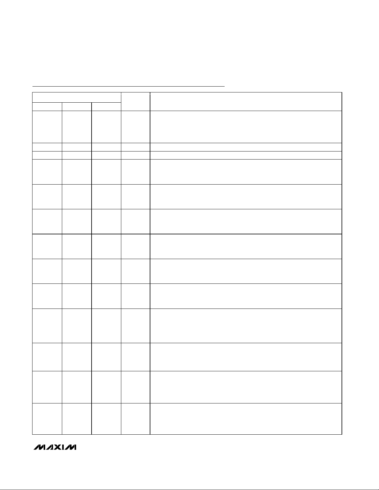
PROGRAMMABLE ARRAY
GPI1
GPI2
GPI3
GPI4 *
MARGIN
MR
TIMING BLOCK 1
TIMING BLOCK 2
TIMING BLOCK 3
TIMING BLOCK 4
TIMING BLOCK 5
TIMING BLOCK 6
TIMING BLOCK 7
TIMING BLOCK 8
TIMING BLOCK 9
TIMING BLOCK 10
MAIN
OSCILLATOR
V
REF
IN2 DETECTOR
IN3 DETECTOR
IN4 DETECTOR
IN5 DETECTOR
IN6 DETECTOR
IN2
IN3
IN4
IN5*
IN6*
IN1
IN_
DETECTOR
PO2 OUTPUT
PO3 OUTPUT
PO4 OUTPUT
PO5 OUTPUT
PO6 OUTPUT
PO7 OUTPUT
PO8 OUTPUT
PO2
PO3
PO4
PO5
PO6*
PO7*
PO8*
PO1
1µF
1µF
2-WIRE
INTERFACE
SDA
SCL
A0
A1
USER
EEPROM
CONFIG
REGISTERS
CONFIG
EEPROM
GND
* FOR MAX6889/MAX6890 ONLY.
** FOR MAX6889 ONLY.
IN7 DETECTORIN7**
IN8 DETECTORIN8**
5.4V
LDO
PO9 OUTPUT
PO10 OUTPUT
PO9**
PO10**
OPEN-DRAIN OR
WEAK PULLUP
SWITCH
2.55V LDO
OUTPUT
10kΩ
PO_ OUTPUT
10µA POWER-UP
PULLDOWN
LO/
HI
EEPROM
CHARGE PUMP
2.55V
LDO
DBP
V
CC
MAX6889
MAX6890
MAX6891
VIRTUAL
DIODES
Functional Diagram
MAX6889/MAX6890/MAX6891
EEPROM-Programmable, Octal/Hex/Quad,
Power-Supply Sequencers/Supervisors
12 ______________________________________________________________________________________
Detailed Description
The MAX6889/MAX6890/MAX6891 EEPROM-configurable, multivoltage supply sequencers/supervisors
monitor several voltage detector inputs and generalpurpose logic inputs, and feature programmable outputs for highly-configurable power-supply sequencing
applications. The MAX6889 features eight voltage
detector inputs and ten programmable outputs. The
MAX6890 features six voltage detector inputs and eight
programmable outputs, while the MAX6891 features
four voltage detector inputs and five programmable
outputs. Manual reset and margin disable inputs simplify board-level testing during the manufacturing
process.
All voltage detectors provide configurable thresholds
for undervoltage detection. The high-voltage input (IN1)
monitors voltages from 1.25V to 7.625V in 25mV increments, or 2.5V to 13.2V in 50mV increments. Inputs
(IN2–IN7) monitor voltages from 0.5V to 3.05V in 10mV
increments, or 1.0V to 5.5V in 20mV increments. An
additional high-voltage input (IN8, MAX6889 only) monitors voltages from 1.25V to 7.625V in 25mV increments, or 2.5V to 15.25V in 50mV increments. To
monitor thresholds from 0.1667V to 1.0167V in 3.3mV
increments, the respective input voltage detector must
be programmed for high impedance (high-Z) and an
external voltage-divider must be connected.
The host controller communicates with the
MAX6889/MAX6890/MAX6891s’ internal 512-bit user
EEPROM, configuration EEPROM, and configuration
registers through an SMBus/I2C-compatible serial interface (see Figure 1).
Programmable output options include active-high, activelow, open drain, and weak pullup. Program each output
to assert on any voltage detector input, general-purpose
logic input, watchdog timer, or manual reset. Programmable timing delay blocks configure each output to wait
between 25µs and 1600ms before deasserting.
The MAX6889/MAX6890/MAX6891 feature a watchdog
timer for added flexibility. Program the watchdog timer to
assert one or more programmable outputs. Program the
watchdog timer to clear on a combination of one GPI_
input and one programmable output, one of the GPI_
inputs only, or one of the programmable outputs only.
The initial and normal watchdog timeout periods are
independently programmable from 6.25ms to 102.4s.
LOGIC NETWORK
FOR PO_
COMPARATORS
MR, GPI_,
MARGIN
IN _
OUTPUT
STAGES
ANALOG
BLOCK
DIGITAL
BLOCK
SERIAL
INTERFACE
REGISTER BANK
BOOT
CONTROLLER
EEPROM
(USER AND CONFIG)
SDA,
SCL
WATCHDOG
TIMER
GPI_
PO_
Figure 1. Top-Level Block Diagram

MAX6889/MAX6890/MAX6891
EEPROM-Programmable, Octal/Hex/Quad,
Power-Supply Sequencers/Supervisors
______________________________________________________________________________________ 13
Powering the
MAX6889/MAX6890/MAX6891
The MAX6889/MAX6890/MAX6891 derive power from
the voltage detector inputs: IN1–IN5 (MAX6889/
MAX6890), IN1–IN4 (MAX6891), or an external V
CC
supply. A virtual diode-ORing scheme selects the positive input that supplies power to the device (see the
Functional Diagram). IN1 must be at least 4V, or one of
IN2–IN5 (MAX6889/MAX6890)/IN2–IN4 (MAX6891)
must be at least 2.7V to ensure device operation. An
internal LDO regulates IN1 down to 5.4V.
The highest input voltage on IN2–IN5 (MAX6889/
MAX6890)/IN2–IN4 (MAX6891) supplies power to the
device, unless V
IN1
> 6.5V, in which case IN1 supplies
power to the device. For 4V < V
IN1
< 6.5V and one of
V
IN2–VIN5
> 2.7V, the input power source cannot be
determined due to the dropout voltage of the LDO.
Internal hysteresis ensures that the supply input that initially powered the device continues to power the device
when multiple input voltages are within 50mV of
each other.
VCCpowers the analog circuitry. Bypass VCCto GND
with a 1µF ceramic capacitor installed as close to the
device as possible. The internal supply voltage, measured at V
CC
, equals the maximum of IN2–IN5 if V
IN1
=
0V, or equals 5.4V when V
IN1
> 6.5V. Do not use the
internally generated V
CC
to provide power to external
circuitry. Power cannot be supplied through highimpedance voltage detector inputs. To externally supply power through VCC:
MAX6889/MAX6890/MAX6891
FEATURE DESCRIPTION
High-Voltage Input IN1
• 2.5V to 13.2V threshold in 50mV increments.
• 1.25V to 7.625V threshold in 25mV increments.
Positive Voltage Input
IN2–IN7 (MAX6889)
IN2–IN6 (MAX6890)
IN2–IN4 (MAX6891)
• 1V to 5.5V threshold in 20mV increments.
• 0.5V to 3.05V threshold in 10mV increments.
• 0.1667V to 1.0167V threshold in 3.3mV increments in high-Z mode.
High-Voltage Input IN8
(MAX6889)
• 2.5V to 15.25V threshold in 50mV increments.
• 1.25V to 7.625V threshold in 25mV increments.
• 0.1667V to 1.0167V threshold in 3.3mV increments in high-Z mode.
Programmable Outputs
PO1–PO10 (MAX6889)
PO1–PO8 (MAX6890)
PO1–PO5 (MAX6891)
• Active-high or active-low.
• Open-drain or weak pullup output.
• Dependent on MR, MARGIN, IN_, GPI_, and WD.
• Programmable reset timeout periods of 25µs, 1.5625ms, 6.25ms, 25ms, 50ms, 200ms, 400ms,
or 1.6s.
General-Purpose Logic Inputs:
GPI1–GPI4
(MAX6889–MAX6890)
GPI1–GPI3 (MAX6891)
• Active-high or active-low logic levels.
• Configure GPI_ as inputs to the watchdog timer or the programmable output stages.
Watchdog Timer
• Clear dependent on any combination of one GPI_ input and one programmable output, a GPI_
input only, or a programmable output only.
• Initial watchdog timeout period of 6.25ms, 25ms, 100ms, 400ms, 1.6s, 6.4s, 25.6s, or 102.4s.
• Normal watchdog timeout period of 6.25ms, 25ms, 100ms, 400ms, 1.6s, 6.4s, 25.6s, or 102.4s.
• Watchdog enable/disable.
Manual Reset Input (MR)
• Forces PO_ into the active output state when MR = GND.
• PO_ deassert after MR releases high and the PO_ timeout period expires.
VCC Power Mode
Programs whether the device is powered from the highest IN_ input or from an external supply
connected to V
CC
.
Write Disable Locks user EEPROM based on PO_.
Configuration Lock Locks configuration registers and EEPROM.
Table 1. Programmable Features

MAX6889/MAX6890/MAX6891
EEPROM-Programmable, Octal/Hex/Quad,
Power-Supply Sequencers/Supervisors
14 ______________________________________________________________________________________
1) Apply a voltage between 2.7V and 5.5V to one of
VCCor IN2–IN5.
2) Program the internal/external VCCpower EEPROM
at AEh, Bit[2] = 1 (see Table 22).
3) Power down the device.
Subsequent power-ups and software reboots require
an externally supplied VCCto ensure the device is fully
operational.
The MAX6889/MAX6890/MAX6891 also generate a digital supply voltage (DBP) for the internal logic circuitry
and the EEPROM. Bypass DBP to GND with a 1µF
ceramic capacitor installed as close to the device as
possible. The nominal DBP output voltage is 2.55V. Do
not use DBP to provide power to external circuitry.
Inputs
The MAX6889/MAX6890/MAX6891 contain multiple
logic and voltage detector inputs. Each voltage detector input is monitored for undervoltage thresholds.
Table 1 summarizes these various inputs. Set the
threshold voltage for each voltage detector input with
registers 00h–07h. Each threshold voltage is an undervoltage threshold. Set the threshold range for each voltage detector with register 08h.
High-Voltage Input (IN1)
IN1 offers threshold voltages of 2.5V to 13.2V in 50mV
increments, or 1.25V to 7.625V in 25mV increments.
Use the following equations to set the threshold voltages for IN1:
where VTHis the desired threshold voltage and x is the
decimal code for the desired threshold (Table 2). For
the 2.5V to 13.2V range, x must equal 214 or less; oth-
erwise the threshold exceeds the maximum operating
voltage of IN1.
IN2–IN7
The IN2–IN7 positive voltage detectors monitor voltages from 1V to 5.5V in 20mV increments, 0.5V to
3.05V in 10mV increments, or 0.1667V to 1.0167V in
3.3mV increments in high-Z mode. Use the following
equations to set the threshold voltages for IN_:
where VTHis the desired threshold voltage and x is the
decimal code for the desired threshold (Table 3). For
the 1V to 5.5V range, x must equal 225 or less; otherwise the threshold exceeds the maximum operating
voltage of IN2–IN7.
High-Voltage Input (IN8)
Configure IN8 to detect positive thresholds from 2.5V to
15.25V in 50mV increments, 1.25V to 7.625V in 25mV
increments, or 0.1667V to 1.0167V in 3.3mV increments
in high-Z mode. Use the following equations to set the
threshold voltages for IN8:
where VTHis the desired threshold voltage and x is the
decimal code for the desired threshold (Table 4).
x
VV
V
for V to V range
x
VV
V
for V to V range
x
VV
V
for V to V high Z range
TH
TH
TH
=
=
=
−
−
−
−
25
005
25 1525
125
0 025
125 7625
0 1667
0 0033
0 1667 1 0167
.
.
..
.
.
..
.
.
..
x
VV
V
for V to V range
x
VV
V
for V to V range
x
VV
V
for V to V high Z range
TH
TH
TH
=
=
=
−
−
−
−
1
002
155
05
01
05 305
0 1667
0 0033
0 1667 1 0167
.
.
.
.
..
.
.
..
x
VV
V
for V to V range
x
VV
V
for V to V range
TH
TH
=
−
=
−
25
005
25 132
125
0 025
125 7625
.
.
..
.
.
..
REGISTER
ADDRESS
EEPROM
BIT
DESCRIPTION
00h 80h [7:0] IN1 undervoltage detector threshold (V1) (see equations in the Inputs section)
08h 88h [0]
IN1 range selection. 0 = 2.5V to 13.2V range in 50mV increments. 1 = 1.25V to 7.625V
range in 25mV increments.
09h 89h [0] Must be set to “0” for normal operation
Table 2. IN1 Threshold Settings
MEMORY
ADDRESS
RANGE

MAX6889/MAX6890/MAX6891
EEPROM-Programmable, Octal/Hex/Quad,
Power-Supply Sequencers/Supervisors
______________________________________________________________________________________ 15
GPI1–GPI4
The GPI1–GPI4 (General-Purpose Input) programmable
logic inputs control power-supply sequencing (programmable outputs), reset/interrupt signaling, and
watchdog functions (see the Configuring the Watchdog
Timer section). Configure GPI1–GPI4 for active-low or
active-high logic (Table 5). GPI1–GPI4 internally pull
down to GND through a 10µA current sink.
MR
The manual reset (MR) input initiates a reset condition.
See Table 6 to program the PO_ outputs to assert when
MR is low. All affected programmable outputs remain
asserted (see the Programmable Outputs section) for
their PO_ timeout periods after MR releases high. An
internal 10µA current source pulls MR to DBP. Leave
MR unconnected or connect to DBP if unused.
MAX6889/MAX6890/MAX6891
REGISTER
ADDRESS
EEPROM
MEMORY
BIT
DESCRIPTION
01h 81h
IN2 undervoltage detector threshold (V2) (see equations in the Inputs section)
02h 82h
IN3 undervoltage detector threshold (V3) (see equations in the Inputs section)
03h 83h
IN4 undervoltage detector threshold (V4) (see equations in the Inputs section)
04h 84h
IN 5 ( M AX 6889/M AX 6890 onl y) und er voltag e d etector thr eshol d ( V 5) ( see equations i n the Inputs secti on)
05h 85h
IN 6 ( M AX 6889/M AX 6890 onl y) und er voltag e d etector thr eshol d ( V 6) ( see equations i n the Inputs secti on)
06h 86h
IN7 (MAX6889 only) undervoltage detector threshold (V7) (see equations in the Inputs section)
[1]
IN2 range selection, 0 = 1V to 5.5V range in 20mV increments, 1 = 0.5V to 3.05V range in
10mV increments
[2]
IN3 range selection, 0 = 1V to 5.5V range in 20mV increments, 1 = 0.5V to 3.05V range in
10mV increments
[3]
IN4 range selection, 0 = 1V to 5.5V range in 20mV increments, 1 = 0.5V to 3.05V range in
10mV increments
[4]
IN5 (MAX6889/MAX6890 only) range selection, 0 = 1V to 5.5V range in 20mV increments, 1 =
0.5V to 3.05V range in 10mV increments
[5]
IN6 (MAX6889/MAX6890 only) range selection, 0 = 1V to 5.5V range in 20mV increments, 1 =
0.5V to 3.05V range in 10mV increments
[6]
IN7 (MAX6889 only) range selection, 0 = 1V to 5.5V range in 20mV increments, 1 = 0.5V to
3.05V range in 10mV increments
08h 88h
[7] Not used
[1]
IN2 input impedance. 0 = normal mode. 1 = high-Z mode, with a 0.1667V to 1.0167V range in
3.3mV increments.
[2]
IN3 input impedance. 0 = normal mode. 1 = high-Z mode, with a 0.1667V to 1.0167V range in
3.3mV increments.
[3]
IN4 input impedance. 0 = normal mode. 1 = high-Z mode, with a 0.1667V to 1.0167V range in
3.3mV increments.
[4]
IN5 input impedance. 0 = normal mode. 1 = high-Z mode, with a 0.1667V to 1.0167V range in
3.3mV increments.
[5]
IN6 input impedance. 0 = normal mode. 1 = high-Z mode, with a 0.1667V to 1.0167V range in
3.3mV increments.
09h 89h
[6]
IN7 input impedance. 0 = normal mode. 1 = high-Z mode, with a 0.1667V to 1.0167V range in
3.3mV increments.
Table 3. IN2–IN7 Threshold Settings
ADDRESS
RANGE
[7:0]
[7:0]
[7:0]
[7:0]
[7:0]
[7:0]

MAX6889/MAX6890/MAX6891
EEPROM-Programmable, Octal/Hex/Quad,
Power-Supply Sequencers/Supervisors
16 ______________________________________________________________________________________
MARGIN
MARGIN allows system-level testing while power supplies exceed the normal ranges. Driving MARGIN low
forces the programmable outputs to hold the last state
while system-level testing occurs. Leave MARGIN
unconnected or connect to DBP if unused. An internal
10µA current source pulls MARGIN to DBP. The state of
each programmable output does not change while
MARGIN = GND. MARGIN overrides MR if both assert
at the same time.
Programmable Outputs
The MAX6889 features ten programmable outputs, the
MAX6890 features eight programmable outputs, and
the MAX6891 features five programmable outputs.
Selectable output stage configurations include: activelow or active-high, open drain, or weak pullup. During
power-up, the programmable outputs pull to GND with
an internal 10µA current sink for 1V < VCC< V
UVLO
.
The programmable outputs remain in their active states
until their respective PO timeout period expires, and all
of the programmed conditions are met for each output.
Any output programmed to depend on no condition
always remains in its active state (Table 17). An output
configured as active-high is considered asserted when
that output is logic-high.
The voltage monitors generate fault signals (logical 0) to
the MAX6889/MAX6890/MAX6891s’ logic array when an
input voltage is below the programmed undervoltage
threshold. For example, the PO3 (Table 9) programmable
output may depend on the IN1 undervoltage threshold,
and the state of GPI1. Write “1”s to R10h[0] and R11h[1]
to configure as indicated. IN1 must be above the undervoltage threshold (Table 2) and GPI1 must be inactive
(Table 5) to be a logic “1,” then PO3 deasserts. The logic
state of PO3, in this example, is equivalent to the logical
statement: “V1 · GPI1.”
Registers 0Ah through 27h configure each of the programmable outputs. Programmable timing blocks set
the PO_ timeout period from 25µs to 1600ms for each
programmable output. See Table 17 to set the active
state (active-high or active-low) for each programmable
output and Tables 18 and 19 to select the output stage
types, and PO_ timeout periods for each output. Each
programmable output allows a different set of conditions to assert each output as shown in Tables 7–16.
REGISTER
ADDRESS
EEPROM
MEMORY
BIT
DESCRIPTION
07h 87h [7:0] IN8 undervoltage detector threshold (V8) (see equations in the Inputs section)
08h 88h [7]
IN8 range selection.
0 = 2.5V to 15.25V range in 50mV increments.
1 = 1.25V to 7.625V range in 25mV increments.
09h 89h [7]
IN8 input impedance. 0 = normal mode. 1 = high-Z mode, with a 0.1667V to 1.0167V
range in 3.3mV increments.
Table 4. IN8 Threshold Settings
REGISTER
ADDRESS
BIT
DESCRIPTION
[0] GPI1. 0 = active-low, 1 = active-high.
[1] GPI2. 0 = active-low, 1 = active-high.
[2] GPI3. 0 = active-low, 1 = active-high.
28h A8h
[3] GPI4 (MAX6889/MAX6890 only). 0 = active-low, 1 = active-high.
Table 5. GPI1–GPI4 Active Logic States
ADDRESS
RANGE
EEPROM
ADDRESS
RANGE

MAX6889/MAX6890/MAX6891
EEPROM-Programmable, Octal/Hex/Quad,
Power-Supply Sequencers/Supervisors
______________________________________________________________________________________ 17
MAX6889/MAX6890/MAX6891
REGISTER
ADDRESS
EEPROM
MEMORY
BIT
DESCRIPTION
0Bh 8Bh [5] PO1. 0 = PO1 independent of MR, 1 = PO1 asserts when MR = low.
0Eh 8Eh [5] PO2. 0 = PO2 independent of MR, 1 = PO2 asserts when MR = low.
11h 91h [5] PO3. 0 = PO3 independent of MR, 1 = PO3 asserts when MR = low.
14h 94h [5] PO4. 0 = PO4/PO2 independent of MR, 1 = PO4 asserts when MR = low.
17h 97h [5] PO5. 0 = PO5 independent of MR, 1 = PO5 asserts when MR = low.
1Ah 9Ah [5]
PO6 (MAX6889/MAX6890 only). 0 = PO6 independent of MR,
1 = PO6 asserts when MR = low.
1Dh 9Dh [5]
PO7 (MAX6889/MAX6890 only). 0 = PO7 independent of MR,
1 = PO7 asserts when MR = low.
20h A0h [5]
PO8 (MAX6889/MAX6890 only). 0 = PO8 independent of MR,
1 = PO8 asserts when MR = low.
23h A3h [5] PO9 (MAX6889 only). 0 = PO9 independent of MR, 1 = PO9 asserts when MR = low.
26h A6h [5] PO10 (MAX6889 only). 0 = PO10 independent of MR, 1 = PO10 asserts when MR = low.
Table 6. Programmable Output Behavior and MR
REGISTER
ADDRESS
EEPROM
MEMORY
BIT OUTPUT ASSERTION CONDITIONS
[0] 1 = PO1 assertion depends on IN1 undervoltage threshold (Table 2)
[1] 1 = PO1 assertion depends on IN2 undervoltage threshold (Table 3)
[2] 1 = PO1 assertion depends on IN3 undervoltage threshold (Table 3)
[3] 1 = PO1 assertion depends on IN4 undervoltage threshold (Table 3)
[4]
1 = PO1 assertion depends on IN5 (MAX6889/MAX6890 only) undervoltage threshold
(Table 3)
[5]
1 = PO1 assertion depends on IN6 (MAX6889/MAX6890 only) undervoltage threshold
(Table 3)
[6] 1 = PO1 assertion depends on IN7 (MAX6890 only) undervoltage threshold (Table 3)
0Ah 8Ah
[7] 1 = PO1 assertion depends on IN8 (MAX6890 only) undervoltage threshold (Table 4)
[0] 1 = PO1 assertion depends on watchdog (Table 20)
[1] 1 = PO1 assertion depends on GPI1 (Table 5)
[2] 1 = PO1 assertion depends on GPI2 (Table 5)
[3] 1 = PO1 assertion depends on GPI3 (Table 5)
[4] 1 = PO1 assertion depends on GPI4 (MAX6889/MAX6890 only) (Table 5)
[5] 1 = PO1 asserts when MR = low (Table 6)
0Bh 8Bh
[7:6] Not used
Table 7. PO1 Output Dependency
Note: Table 7 only applies to PO1. Write a “0” to a bit to make the PO1 output independent of the respective signal (IN_ thresholds,
WD, GPI_, or
MR
).
ADDRESS
RANGE
ADDRESS

MAX6889/MAX6890/MAX6891
EEPROM-Programmable, Octal/Hex/Quad,
Power-Supply Sequencers/Supervisors
18 ______________________________________________________________________________________
REGISTER
ADDRESS
EEPROM
MEMORY
BIT OUTPUT ASSERTION CONDITIONS
[0] 1 = PO2 assertion depends on IN1 undervoltage threshold (Table 2)
[1] 1 = PO2 assertion depends on IN2 undervoltage threshold (Table 3)
[2] 1 = PO2 assertion depends on IN3 undervoltage threshold (Table 3)
[3] 1 = PO2 assertion depends on IN4 undervoltage threshold (Table 3)
[4]
1 = PO2 assertion depends on IN5 (MAX6889/MAX6890 only) undervoltage threshold
(Table 3)
[5]
1 = PO2 assertion depends on IN6 (MAX6889/MAX6890 only) undervoltage threshold
(Table 3)
[6] 1 = PO2 assertion depends on IN7 (MAX6890 only) undervoltage threshold (Table 3)
0Dh 8Dh
[7] 1 = PO2 assertion depends on IN8 (MAX6890 only) undervoltage threshold (Table 4)
[0] 1 = PO2 assertion depends on watchdog (Table 20)
[1] 1 = PO2 assertion depends on GPI1 (Table 5)
[2] 1 = PO2 assertion depends on GPI2 (Table 5)
[3] 1 = PO2 assertion depends on GPI3 (Table 5)
[4] 1 = PO2 assertion depends on GPI4 (MAX6889/MAX6890 only) (Table 5)
[5] 1 = PO2 asserts when MR = low (Table 6)
0Eh 8Eh
[7:6] Not used
Table 8. PO2 Output Dependency
Note: Table 8 only applies to PO2. Write a “0” to a bit to make the PO2 output independent of the respective signal (IN_ thresholds,
WD, GPI_, or
MR
).
ADDRESS

MAX6889/MAX6890/MAX6891
EEPROM-Programmable, Octal/Hex/Quad,
Power-Supply Sequencers/Supervisors
______________________________________________________________________________________ 19
REGISTER
ADDRESS
EEPROM
MEMORY
BIT OUTPUT ASSERTION CONDITIONS
[0] 1 = PO3 assertion depends on IN1 undervoltage threshold (Table 2)
[1] 1 = PO3 assertion depends on IN2 undervoltage threshold (Table 3)
[2] 1 = PO3 assertion depends on IN3 undervoltage threshold (Table 3)
[3] 1 = PO3 assertion depends on IN4 undervoltage threshold (Table 3)
[4]
1 = PO3 assertion depends on IN5 (MAX6889/MAX6890 only) undervoltage threshold
(Table 3)
[5]
1 = PO3 assertion depends on IN6 (MAX6889/MAX6890 only) undervoltage threshold
(Table 3)
[6] 1 = PO3 assertion depends on IN7 (MAX6890 only) undervoltage threshold (Table 3)
10h 90h
[7] 1 = PO3 assertion depends on IN8 (MAX6890 only) undervoltage threshold (Table 4)
[0] 1 = PO3 assertion depends on watchdog (Table 20)
[1] 1 = PO3 assertion depends on GPI1 (Table 5)
[2] 1 = PO3 assertion depends on GPI2 (Table 5)
[3] 1 = PO3 assertion depends on GPI3 (Table 5)
[4] 1 = PO3 assertion depends on GPI4 (MAX6889/MAX6890 only) (Table 5)
[5] 1 = PO3 asserts when MR = low (Table 6)
11h 11h
[7:6] Not used
Table 9. PO3 Output Dependency
Note: Table 9 only applies to PO3. Write a “0” to a bit to make the PO3 output independent of the respective signal (IN_ thresholds,
WD, GPI_, or
MR
).
ADDRESS

MAX6889/MAX6890/MAX6891
EEPROM-Programmable, Octal/Hex/Quad,
Power-Supply Sequencers/Supervisors
20 ______________________________________________________________________________________
REGISTER
ADDRESS
EEPROM
MEMORY
BIT OUTPUT ASSERTION CONDITIONS
[0] 1 = PO4 assertion depends on IN1 undervoltage threshold (Table 2)
[1] 1 = PO4 assertion depends on IN2 undervoltage threshold (Table 3)
[2] 1 = PO4 assertion depends on IN3 undervoltage threshold (Table 3)
[3] 1 = PO4 assertion depends on IN4 undervoltage threshold (Table 3)
[4]
1 = PO4 assertion depends on IN5 (MAX6889/MAX6890 only) undervoltage threshold
(Table 3)
[5]
1 = PO4 assertion depends on IN6 (MAX6889/MAX6890 only) undervoltage threshold
(Table 3)
[6] 1 = PO4 assertion depends on IN7 (MAX6890 only) undervoltage threshold (Table 3)
13h 93h
[7] 1 = PO4 assertion depends on IN8 (MAX6890 only) undervoltage threshold (Table 4)
[0] 1 = PO4 assertion depends on watchdog (Table 20)
[1] 1 = PO4 assertion depends on GPI1 (Table 5)
[2] 1 = PO4 assertion depends on GPI2 (Table 5)
[3] 1 = PO4 assertion depends on GPI3 (Table 5)
[4] 1 = PO4 assertion depends on GPI4 (MAX6889/MAX6890 only) (Table 5)
[5] 1 = PO4 asserts when MR = low (Table 6)
14h 14h
[7:6] Not used
Table 10. PO4 Output Dependency
Note: Table 10 only applies to PO4. Write a “0” to a bit to make the PO4 output independent of the respective signal (IN_ thresholds,
WD, GPI_, or
MR
).
ADDRESS

MAX6889/MAX6890/MAX6891
EEPROM-Programmable, Octal/Hex/Quad,
Power-Supply Sequencers/Supervisors
______________________________________________________________________________________ 21
REGISTER
ADDRESS
EEPROM
MEMORY
BIT OUTPUT ASSERTION CONDITIONS
[0] 1 = PO5 assertion depends on IN1 undervoltage threshold (Table 2)
[1] 1 = PO5 assertion depends on IN2 undervoltage threshold (Table 3)
[2] 1 = PO5 assertion depends on IN3 undervoltage threshold (Table 3)
[3] 1 = PO5 assertion depends on IN4 undervoltage threshold (Table 3)
[4]
1 = PO5 assertion depends on IN5 (MAX6889/MAX6890 only) undervoltage threshold
(Table 3)
[5]
1 = PO5 assertion depends on IN6 (MAX6889/MAX6890 only) undervoltage threshold
(Table 3)
[6] 1 = PO5 assertion depends on IN7 (MAX6890 only) undervoltage threshold (Table 3)
16h 96h
[7] 1 = PO5 assertion depends on IN8 (MAX6890 only) undervoltage threshold (Table 4)
[0] 1 = PO5 assertion depends on watchdog (Table 20)
[1] 1 = PO5 assertion depends on GPI1 (Table 5)
[2] 1 = PO5 assertion depends on GPI2 (Table 5)
[3] 1 = PO5 assertion depends on GPI3 (Table 5)
[4] 1 = PO5 assertion depends on GPI4 (MAX6889/MAX6890 only) (Table 5)
[5] 1 = PO5 asserts when MR = low (Table 6)
17h 17h
[7:6] Not used
Table 11. PO5 Output Dependency
Note: Table 11 only applies to PO5. Write a “0” to a bit to make the PO5 output independent of the respective signal (IN_ thresholds,
WD, GPI_, or
MR
).
ADDRESS

MAX6889/MAX6890/MAX6891
EEPROM-Programmable, Octal/Hex/Quad,
Power-Supply Sequencers/Supervisors
22 ______________________________________________________________________________________
REGISTER
ADDRESS
EEPROM
MEMORY
BIT OUTPUT ASSERTION CONDITIONS
[0] 1 = PO7 assertion depends on IN1 undervoltage threshold (Table 2)
[1] 1 = PO7 assertion depends on IN2 undervoltage threshold (Table 3)
[2] 1 = PO7 assertion depends on IN3 undervoltage threshold (Table 3)
[3] 1 = PO7 assertion depends on IN4 undervoltage threshold (Table 3)
[4] 1 = PO7 assertion depends on IN5 undervoltage threshold (Table 3)
[5] 1 = PO7 assertion depends on IN6 undervoltage threshold (Table 3)
[6] 1 = PO7 assertion depends on IN7 (MAX6890 only) undervoltage threshold (Table 3)
1Ch 9Ch
[7] 1 = PO7 assertion depends on IN8 (MAX6890 only) undervoltage threshold (Table 4)
[0] 1 = PO7 assertion depends on watchdog (Table 20)
[1] 1 = PO7 assertion depends on GPI1 (Table 5)
[2] 1 = PO7 assertion depends on GPI2 (Table 5)
[3] 1 = PO7 assertion depends on GPI3 (Table 5)
[4] 1 = PO7 assertion depends on GPI4 (Table 5)
[5] 1 = PO7 asserts when MR = low (Table 6)
1Dh 9Dh
[7:6] Not used
Table 13. PO7 (MAX6889/MAX6890 Only) Output Dependency
Note: Table 13 only applies to PO7 (MAX6889/MAX6890 only). Write a “0” to a bit to make the PO7 output independent of the
respective signal (IN_ thresholds, WD, GPI_, or
MR
).
REGISTER
ADDRESS
EEPROM
MEMORY
BIT OUTPUT ASSERTION CONDITIONS
[0] 1 = PO6 assertion depends on IN1 undervoltage threshold (Table 2)
[1] 1 = PO6 assertion depends on IN2 undervoltage threshold (Table 3)
[2] 1 = PO6 assertion depends on IN3 undervoltage threshold (Table 3)
[3] 1 = PO6 assertion depends on IN4 undervoltage threshold (Table 3)
[4] 1 = PO6 assertion depends on IN5 undervoltage threshold (Table 3)
[5] 1 = PO6 assertion depends on IN6 undervoltage threshold (Table 3)
[6] 1 = PO6 assertion depends on IN7 (MAX6890 only) undervoltage threshold (Table 3)
19h 99h
[7] 1 = PO6 assertion depends on IN8 (MAX6890 only) undervoltage threshold (Table 4)
[0] 1 = PO6 assertion depends on watchdog (Table 20)
[1] 1 = PO6 assertion depends on GPI1 (Table 5)
[2] 1 = PO6 assertion depends on GPI2 (Table 5)
[3] 1 = PO6 assertion depends on GPI3 (Table 5)
[4] 1 = PO6 assertion depends on GPI4 (Table 5)
[5] 1 = PO4 asserts when MR = low (Table 6)
1Ah 9Ah
[7:6] Not used
Table 12. PO6 (MAX6889/MAX6890 Only) Output Dependency
Note: Table 12 only applies to PO6 (MAX6889/MAX6890 only). Write a “0” to a bit to make the PO6 output independent of the
respective signal (IN_ thresholds, WD, GPI_, or
MR
).
ADDRESS
ADDRESS

MAX6889/MAX6890/MAX6891
EEPROM-Programmable, Octal/Hex/Quad,
Power-Supply Sequencers/Supervisors
______________________________________________________________________________________ 23
REGISTER
ADDRESS
EEPROM
MEMORY
BIT OUTPUT ASSERTION CONDITIONS
[0] 1 = PO9 assertion depends on IN1 undervoltage threshold (Table 2)
[1] 1 = PO9 assertion depends on IN2 undervoltage threshold (Table 3)
[2] 1 = PO9 assertion depends on IN3 undervoltage threshold (Table 3)
[3] 1 = PO9 assertion depends on IN4 undervoltage threshold (Table 3)
[4] 1 = PO9 assertion depends on IN5 undervoltage threshold (Table 3)
[5] 1 = PO9 assertion depends on IN6 undervoltage threshold (Table 3)
[6] 1 = PO9 assertion depends on IN7 undervoltage threshold (Table 3)
22h A2h
[7] 1 = PO9 assertion depends on IN8 undervoltage threshold (Table 4)
[0] 1 = PO9 assertion depends on watchdog (Table 20)
[1] 1 = PO9 assertion depends on GPI1 (Table 5)
[2] 1 = PO9 assertion depends on GPI2 (Table 5)
[3] 1 = PO9 assertion depends on GPI3 (Table 5)
[4] 1 = PO9 assertion depends on GPI4 (Table 5)
[5] 1 = PO9 asserts when MR = low (Table 6)
23h A3h
[7:6] Not used
Table 15. PO9 (MAX6889 Only) Output Dependency
Note: Table 15 only applies to PO9 (MAX6889 only). Write a “0” to a bit to make the PO9 output independent of the respective signal
(IN_ thresholds, WD, GPI_, or
MR
).
REGISTER
ADDRESS
EEPROM
MEMORY
BIT OUTPUT ASSERTION CONDITIONS
[0] 1 = PO8 assertion depends on IN1 undervoltage threshold (Table 2)
[1] 1 = PO8 assertion depends on IN2 undervoltage threshold (Table 3)
[2] 1 = PO8 assertion depends on IN3 undervoltage threshold (Table 3)
[3] 1 = PO8 assertion depends on IN4 undervoltage threshold (Table 3)
[4] 1 = PO8 assertion depends on IN5 undervoltage threshold (Table 3)
[5] 1 = PO8 assertion depends on IN6 undervoltage threshold (Table 3)
[6] 1 = PO8 assertion depends on IN7 (MAX6890 only) undervoltage threshold (Table 3)
1Fh 9Fh
[7] 1 = PO8 assertion depends on IN8 (MAX6890 only) undervoltage threshold (Table 4)
[0] 1 = PO8 assertion depends on watchdog (Table 20)
[1] 1 = PO8 assertion depends on GPI1 (Table 5)
[2] 1 = PO8 assertion depends on GPI2 (Table 5)
[3] 1 = PO8 assertion depends on GPI3 (Table 5)
[4] 1 = PO8 assertion depends on GPI4 (Table 5)
[5] 1 = PO8 asserts when MR = low (Table 6)
20h A0h
[7:6] Not used
Table 14. PO8 (MAX6889/MAX6890 Only) Output Dependency
Note: Table 14 only applies to PO8 (MAX6889/MAX6890 only). Write a “0” to a bit to make the PO8 output independent of the
respective signal (IN_ thresholds, WD, GPI_, or
MR
).
ADDRESS
ADDRESS

MAX6889/MAX6890/MAX6891
EEPROM-Programmable, Octal/Hex/Quad,
Power-Supply Sequencers/Supervisors
24 ______________________________________________________________________________________
REGISTER
ADDRESS
EEPROM
MEMORY
BIT OUTPUT ASSERTION CONDITIONS
[0] 1 = PO10 assertion depends on IN1 undervoltage threshold (Table 2)
[1] 1 = PO10 assertion depends on IN2 undervoltage threshold (Table 3)
[2] 1 = PO10 assertion depends on IN3 undervoltage threshold (Table 3)
[3] 1 = PO10 assertion depends on IN4 undervoltage threshold (Table 3)
[4] 1 = PO10 assertion depends on IN5 undervoltage threshold (Table 3)
[5] 1 = PO10 assertion depends on IN6 undervoltage threshold (Table 3)
[6] 1 = PO10 assertion depends on IN7 undervoltage threshold (Table 3)
25h A5h
[7] 1 = PO10 assertion depends on IN8 undervoltage threshold (Table 4)
[0] 1 = PO10 assertion depends on watchdog (Table 20)
[1] 1 = PO10 assertion depends on GPI1 (Table 5)
[2] 1 = PO10 assertion depends on GPI2 (Table 5)
[3] 1 = PO10 assertion depends on GPI3 (Table 5)
[4] 1 = PO10 assertion depends on GPI4 (Table 5)
[5] 1 = PO10 asserts when MR = low (Table 6)
26h A6h
[7:6] Not used
Table 16. PO10 (MAX6889 Only) Output Dependency
Note: Table 16 only applies to PO10 (MAX6890 only). Write a “0” to a bit to make the PO10 output independent of the respective signal (IN_ thresholds, WD, GPI_, or
MR
).
REGISTER
ADDRESS
EEPROM
MEMORY
BIT
AFFECTED
DESCRIPTION
0Ch 8Ch [1] PO1 0 = active-low, 1 = active-high
0Fh 8Fh [1] PO2 0 = active-low, 1 = active-high
12h 92h [1] PO3 0 = active-low, 1 = active-high
15h 95h [1] PO4 0 = active-low, 1 = active-high
18h 98h [1] PO5 0 = active-low, 1 = active-high
1Bh 9Bh [1] PO6 MAX6889/MAX6890 only. 0 = active-low, 1 = active-high.
1Eh 9Eh [1] PO7 MAX6889/MAX6890 only. 0 = active-low, 1 = active-high.
21h A1h [1] PO8 MAX6889/MAX6890 only. 0 = active-low, 1 = active-high.
24h A4h [1] PO9 MAX6889 only. 0 = active-low, 1 = active-high.
27h A7h [1] PO10 MAX6889 only. 0 = active-low, 1 = active-high.
Table 17. Programmable Output Active States
ADDRESS
ADDRESS
RANGE
OUTPUT

MAX6889/MAX6890/MAX6891
EEPROM-Programmable, Octal/Hex/Quad,
Power-Supply Sequencers/Supervisors
______________________________________________________________________________________ 25
Output Stage Configurations
Independently configure each programmable output as
active-high or active-low (Table 17). Additionally, configure each programmable output as open drain or weak
pullup (Table 18). Finally, set the PO_ timeout period for
each programmable output (Table 19). The programmable outputs can sink up to 4mA.
Weak Pullup Output Configuration
The MAX6889/MAX6890/MAX6891s’ programmable outputs
have a pullup resistance (10kΩ, typ) connected to the internal 2.55V LDO output to provide weak pullup outputs.
Open-Drain Output Configuration
Connect an external pullup resistor from the programmable output to an external voltage when configured as
an open-drain output. Open-drain configured outputs
may be pulled up to 13.2V. Choose the pullup resistor
depending on the number of devices connected to the
open-drain output and the allowable current consumption. The open-drain output configuration allows wireORed connections, and provides flexibility in setting the
pullup current.
Configuring the Watchdog Timer
(Registers 29h–2Ah)
A watchdog timer monitors microprocessor software
execution for a stalled condition and resets the microprocessor if it stalls. The output of the watchdog timer
(one of the programmable outputs) connects to the reset
input or a nonmaskable interrupt of the microprocessor.
Registers 29h–2Ah configure the watchdog functionality of the MAX6889/MAX6890/MAX6891. Program the
watchdog timer to assert one or more programmable
outputs (see Tables 7–16). Program the watchdog timer
to reset on one of the GPI_ inputs, one of the programmable outputs, or a combination of one GPI_ input and
one programmable output.
The watchdog timer features independent initial and
normal watchdog timeout periods. The initial watchdog
timeout period applies immediately after power-up,
after a software reboot, after a reset event takes place,
or after enabling the watchdog timer. The initial watchdog timeout period allows the microprocessor to per-
form its initialization process. If no pulse occurs during
the initial watchdog timeout period, the microprocessor
is taking too long to initialize, indicating a potential
problem.
The normal watchdog timeout period applies after the
initial watchdog timeout period occurs. The normal
watchdog timeout period monitors a pulsed output of
the microprocessor that indicates when normal processor behavior occurs. If no pulse occurs during the normal watchdog timeout period, this indicates that the
processor has stopped operating or is stuck in an infinite execution loop.
Register 2Ah programs the initial and normal watchdog
timeout periods, and enables or disables the watchdog
timer. See Tables 20 and 21 for a summary of the
watchdog behavior.
Configuration Lock
Lock the configuration register bank and configuration
EEPROM contents after initial programming by setting
the lock bit high (see Table 22). Locking the configuration prevents write operations to all registers except the
configuration lock register. Clear the lock bit to reconfigure the device.
Internal/External VCCPower
The MAX6889/MAX6890/MAX6891 can generate an
internal VCC, or VCCcan be externally supplied (see
Table 22). To internally generate VCCfrom the highest
voltage on IN1–IN5 set register 2Eh and EEPROM
address AEh Bit[2] = 0. To use an externally supplied,
always-on VCCensure register 2Eh and EEPROM
address AEh Bit[2] =1 (see the Powering the MAX6889/
MAX6890/MAX6891 section).
Write Disable
A unique write-disable feature protects the MAX6889/
MAX6890/MAX6891 from inadvertent user-EEPROM
writes. As input voltages that power the serial interface,
a microprocessor, or any other writing-devices fall,
unintentional data may be written onto the data bus.
The user-EEPROM write-disable function (see Table 23)
ensures that unintentional data does not corrupt the
MAX6889/MAX6890/MAX6891 EEPROM data.

MAX6889/MAX6890/MAX6891
EEPROM-Programmable, Octal/Hex/Quad,
Power-Supply Sequencers/Supervisors
26 ______________________________________________________________________________________
REGISTER
ADDRESS
EEPROM
MEMORY
BIT
AFFECTED
DESCRIPTION
0Ch 8Ch [0] PO1 0 = weak pullup, 1 = open drain
0Fh 8Fh [0] PO2 0 = weak pullup, 1 = open drain
12h 92h [0] PO3 0 = weak pullup, 1 = open drain
15h 95h [0] PO4 0 = weak pullup, 1 = open drain
18h 98h [0] PO5 0 = weak pullup, 1 = open drain
1Bh 9Bh [0] PO6 MAX6889/MAX6890 only. 0 = weak pullup, 1 = open drain.
1Eh 9Eh [0] PO7 MAX6889/MAX6890 only. 0 = weak pullup, 1 = open drain.
21h A1h [0] PO8 MAX6889/MAX6890 only. 0 = weak pullup, 1 = open drain.
24h A4h [0] PO9 MAX6889 only. 0 = weak pullup, 1 = open drain.
27h A7h [0] PO10 MAX6889 only. 0 = weak pullup, 1 = open drain.
Table 18. Programmable Output Stage Options
REGISTER
ADDRESS
EEPROM
MEMORY
BIT
AFFECTED OUTPUTS DESCRIPTION
0Ch 8Ch [4:2] PO1
0Fh 8Fh [4:2] PO2
12h 92h [4:2] PO3
15h 95h [4:2] PO4
18h 98h [4:2] PO5
1Bh 9Bh [4:2] PO6 (MAX6889/MAX6890)
1Eh 9Eh [4:2] PO7 (MAX6889/MAX6890)
21h A1h [4:2] PO8 (MAX6889/MAX6890)
24h A4h [4:2] PO9 (MAX6889 only)
27h A7h [4:2] PO10 (MAX6889 only)
000 = 25µs
001 = 1.5625ms
010 = 6.25ms
011 = 25ms
100 = 50ms
101 = 200ms
110 = 400ms
111 = 1600ms
Table 19. PO_ Timeout Periods
ADDRESS
RANGE
OUTPUT
ADDRESS
RANGE

MAX6889/MAX6890/MAX6891
EEPROM-Programmable, Octal/Hex/Quad,
Power-Supply Sequencers/Supervisors
______________________________________________________________________________________ 27
REGISTER
ADDRESS
EEPROM
MEMORY
BIT
DESCRIPTION
[1:0]
Watchdog Input Selection:
00 = GPI1 input
01 = GPI2 input
10 = GPI3 input
11 = GPI4 input (MAX6889/MAX6890 only). Selects GPI3 on MAX6891.
[5:2]
Watchdog Internal Input Selection:
0000 = PO1
0001 = PO2
0010 = PO3
0011 = PO4
0100 = PO5
0101 = PO6 (MAX6889/MAX6890 only)
0110 = PO7 (MAX6889/MAX6890 only)
0111 = PO8 (MAX6889/MAX6890 only)
1000 = PO9 (MAX6889 only)
1001 = PO10 (MAX6889 only)
[1011] to [1111] = WD is not affected by PO_
29h A9h
[7:6]
Watchdog Dependency on Inputs:
00 = Watchdog not dependent on any input
01 = Watchdog clear depends on selected GPI_ input only
01 = Watchdog clear depends on selected PO_ input only
11 = Watchdog clear depends on both selected GPI_ and PO_ inputs
Table 20. Watchdog Inputs
ADDRESS
RANGE

MAX6889/MAX6890/MAX6891
EEPROM-Programmable, Octal/Hex/Quad,
Power-Supply Sequencers/Supervisors
28 ______________________________________________________________________________________
REGISTER
ADDRESS
EEPROM
MEMORY
BIT
DESCRIPTION
[2:0]
Normal Watchdog Timeout Period:
000 = 6.25ms
001 = 25ms
010 = 100ms
011 = 400ms
100 = 1.6s
101 = 6.4s
110 = 25.6s
111 = 102.4s
[5:3]
Initial Watchdog Timeout Period (immediately following power-up, reset event, or enabling
watchdog):
000 = 6.25ms
001 = 25ms
010 = 100ms
011 = 400ms
100 = 1.6s
101 = 6.4s
110 = 25.6s
111 = 102.4s
[6]
Watchdog Enable
0 = Disables watchdog timer
1 = Enables watchdog timer
2Ah AAh
[7] Not used
Table 21. Watchdog Timeout Period Selection
REGISTER
ADDRESS
EEPROM
MEMORY
BIT
DESCRIPTION
[0]
0 = Configuration unlocked
1 = Configuration locked
[1] Not used
[2]
Internal/External V
CC
Power:
0 = V
CC
internally generated
1 = V
CC
externally supplied
2Eh AEh
[7:3] Not used
Table 22. Configuration Lock and Internal/External VCCPower Register
ADDRESS
RANGE
ADDRESS
RANGE

MAX6889/MAX6890/MAX6891
EEPROM-Programmable, Octal/Hex/Quad,
Power-Supply Sequencers/Supervisors
______________________________________________________________________________________ 29
REGISTER
ADDRESS
EEPROM
MEMORY
BIT
DESCRIPTION
[0]
0 = Write is not disabled if PO1 asserts
1 = Write disabled if PO1 asserts
[1]
0 = Write is not disabled if PO2 asserts
1 = Write disabled if PO2 asserts
[2]
0 = Write is not disabled if PO3 asserts
1 = Write disabled if PO3 asserts
[3]
0 = Write is not disabled if PO4 asserts
1 = Write disabled if PO4 asserts
[4]
0 = Write is not disabled if PO5 asserts
1 = Write disabled if PO5 asserts
[5]
0 = Write is not disabled if PO6 asserts
1 = Write disabled if PO6 asserts
[6]
0 = Write is not disabled if PO7 asserts
1 = Write disabled if PO7 asserts
2Ch ACh
[7]
0 = Write is not disabled if PO8 asserts
1 = Write disabled if PO8 asserts
[0]
0 = Write is not disabled if PO9 asserts
1 = Write disabled if PO9 asserts
[1]
0 = Write is not disabled if PO10 asserts
1 = Write disabled if PO10 asserts
2Dh ADh
[7:2] Not used
Table 23. Write Disable Register
Configuring the
MAX6889/MAX6890/MAX6891
The MAX6889/MAX6890/MAX6891 factory-default configuration sets all registers to 0h, except bits in Tables
17 and 18, which are set to 1h. Factory-default configuration sets all PO_’s as active-high, open drain (all outputs are high impedance until the device is configured
by the user). Each device requires configuration before
full power is applied to the system. To configure the
MAX6889/MAX6890/MAX6891, first apply an input voltage to IN1, or one of IN2–IN5 or V
CC
(see the Powering
the MAX6889/MAX6890/MAX6891 section). V
IN1
> 4V,
or one of V
IN2–VIN5
or VCC> 2.7V to ensure device
operation. Next, transmit data through the serial interface. Use the block write protocol to quickly configure
the device. Write to the configuration registers first to
ensure the device is configured properly. After completing the setup procedure, use the read word or
block read protocol to read back the data from the configuration registers. Lastly, use the write byte or block
write protocol to write this data to the EEPROM registers. After completing the EEPROM register configuration, apply full power to the system to begin normal
operation. The nonvolatile EEPROM stores the latest
configuration upon removal of power. Write 0s to all
EEPROM registers to clear the memory.
Software Reboot
A software reboot allows the user to restore the EEPROM
configuration to the volatile registers without cycling the
power supplies. Use the send byte command with data
byte C4h to initiate a software reboot. The 3ms (max)
power-up delay also applies after a software reboot.
Configuration EEPROM
The configuration EEPROM addresses range from 80h
to AEh. Write data to the configuration EEPROM to automatically set up the MAX6889/MAX6890/MAX6891 upon
power-up. Data is transferred from the configuration
EEPROM to the configuration registers when V
CC
exceeds UVLO during power-up or after a software
ADDRESS
RANGE

MAX6889/MAX6890/MAX6891
EEPROM-Programmable, Octal/Hex/Quad,
Power-Supply Sequencers/Supervisors
30 ______________________________________________________________________________________
STOP
CONDITION
REPEATED START
CONDITION
START
CONDITION
t
HIGH
t
LOW
t
R
t
F
t
SU:DAT
t
SU:STA
t
SU:STO
t
HD:STA
t
BUF
t
HD:STA
t
HD:DAT
SCL
SDA
START
CONDITION
Figure 3. Serial-Interface Timing Details
reboot. After VCCexceeds UVLO, an internal 1MHz
clock starts after a 5µs delay, and data transfer begins.
Data transfer disables access to the configuration registers and EEPROM. The data transfer from EEPROM to
configuration registers takes 3ms (max). Read configuration EEPROM data at any time after power-up or software reboot. Write commands to the configuration
EEPROM are allowed at any time after power-up or software reboot, unless the configuration lock bit is set (see
Table 22). The maximum cycle time to write a single
byte is 11ms (max).
User EEPROM
The 512-bit, user-EEPROM addresses range from 40h to
7Fh (see Figure 2). Store software revision data, board
revision data, and other data in these registers. The maximum cycle time to write a single byte is 11ms (max).
Configuration Register Bank and EEPROM
The configuration registers can be directly modified
through the serial interface without modifying the
EEPROM, after the power-up procedure terminates and
the configuration EEPROM data has been loaded into the
configuration register bank. Use the write byte or block
write protocols to write directly to the configuration registers. Changes to the configuration registers take effect
immediately and are lost upon power removal.
At device power-up, the register bank loads configuration data from the EEPROM. Configuration data may be
directly altered in the register bank during application
development, allowing maximum flexibility. Transfer the
new configuration data byte-by-byte to the configuration EEPROM with the write byte protocol. The next
device power-up or software reboot automatically loads
the new configuration.
SMBus/I2C-Compatible Serial Interface
The MAX6889/MAX6890/MAX6891 feature an I2C/SMBuscompatible 2-wire serial interface consisting of a serial
data line (SDA) and a serial clock line (SCL). SDA and
SCL facilitate bidirectional communication between the
MAX6889/MAX6890/MAX6891 and the master device at
clock rates up to 400kHz. Figure 3 shows the 2-wire interface timing diagram. The MAX6889/MAX6890/MAX6891
are transmit/receive slave-only devices, relying upon a
40h
USER EEPROM
7Fh
80h
CONFIGURATION
EEPROM
AEh
00h
REGISTER BANK
37h
RESERVED
Figure 2. Memory Map

MAX6889/MAX6890/MAX6891
EEPROM-Programmable, Octal/Hex/Quad,
Power-Supply Sequencers/Supervisors
______________________________________________________________________________________ 31
MAX6889/MAX6890/MAX6891MAX6889/MAX6890/MAX6891MAX6889/MAX6890/MAX6891
master device to generate a clock signal. The master
device (typically a microcontroller) generates SCL and initiates data transfer on the bus.
A master device communicates to the MAX6889/
MAX6890/MAX6891 by transmitting the proper address
followed by command and/or data words. Each transmit sequence is framed by a START (S) or REPEATED
START (SR) condition and a STOP (P) condition. Each
word transmitted over the bus is 8 bits long and is
always followed by an acknowledge pulse.
SCL is a logic input, while SDA is an open-drain
input/output. SCL and SDA both require external pullup
resistors to generate the logic-high voltage. Use 4.7kΩ
resistors for most applications.
Bit Transfer
Each clock pulse transfers one data bit. The data on
SDA must remain stable while SCL is high (Figure 4),
otherwise the MAX6889/MAX6890/MAX6891 register a
START or STOP condition (Figure 5) from the master.
SDA and SCL idle high when the bus is not busy.
Start and Stop Conditions
A master device signals the beginning of a transmission
with a START (S) condition (Figure 5) by transitioning
SDA from high to low while SCL is high. The master
device issues a STOP (P) condition (Figure 5) by transitioning SDA from low to high while SCL is high. A STOP
condition frees the bus for another transmission. The bus
remains active if a REPEATED START condition is generated, such as in the read byte or block read protocol
(see Figure 8). Both SCL and SDA are high when the bus
is not busy.
Early STOP Conditions
The MAX6889/MAX6890/MAX6891 recognize a STOP
condition at any point during transmission except if a
STOP condition occurs in the same high pulse as a
START condition. This condition is not a legal I2C format. At least one clock pulse must separate any START
and STOP condition.
Repeated START Conditions
A REPEATED START (SR) condition may indicate a
change of data direction on the bus. Such a change
occurs when a command word is required to initiate a
read operation (see Figure 8). SR may also be used
when the bus master is writing to several I2C devices
and does not want to relinquish control of the bus. The
MAX6889/MAX6890/MAX6891 serial interface supports
continuous write operations with or without an SR condition separating them. Continuous read operations
require SR conditions because of the change in direction
of data flow.
Acknowledge
The acknowledge bit (ACK) is the 9th bit attached to any
8-bit data word. The receiving device always generates
an ACK. The MAX6889/MAX6890/MAX6891 generate an
ACK when receiving an address or data by pulling SDA
low during the 9th clock period (Figure 6). When transmitting data, such as when the master device reads data
back from the MAX6889/MAX6890/MAX6891, the
MAX6889/MAX6890/MAX6891 wait for the master device
to generate an ACK. Monitoring ACK allows for detection
of unsuccessful data transfers. An unsuccessful data
transfer occurs if the receiving device is busy or if a system fault has occurred. In the event of an unsuccessful
DATA LINE STABLE,
DATA VALID
SDA
SCL
CHANGE OF
DATA ALLOWED
Figure 4. Bit Transfer
PS
START
CONDITION
SDA
SCL
STOP
CONDITION
Figure 5. Start and Stop Conditions

MAX6889/MAX6890/MAX6891
EEPROM-Programmable, Octal/Hex/Quad,
Power-Supply Sequencers/Supervisors
32 ______________________________________________________________________________________
data transfer, the bus master should reattempt communication at a later time. The MAX6889/MAX6890/
MAX6891 generate a NACK after the command byte
during a software reboot, while writing to the EEPROM,
or when receiving an illegal memory address.
Slave Address
SA7 through SA4 represent the standard 2-wire interface address (1010) for devices with EEPROM. SA3
and SA2 correspond to the A1 and A0 address inputs
of the MAX6889/MAX6890/MAX6891 (hardwired as
logic-low or logic-high). SA0 is a read/write flag bit (0 =
write, 1 = read).
The A0 and A1 address inputs allow up to four
MAX6889/MAX6890 to connect to one bus, while the
A0 address input allows up to two MAX6891s to con-
nect to one bus. Connect A0 and A1 to GND or to the
2-wire serial-interface power supply (see Figure 7).
SCL
1
S
2
89
SDA BY
TRANSMITTER
SDA BY
RECEIVER
START
CONDITION
CLOCK PULSE FOR ACKNOWLEDGE
Figure 6. Acknowledge
SDA
SCL
1
MSB LSBSTART
01
0
A1
A0
XR/W
ACK
Figure 7. Slave Address
The MAX6889/MAX6890 slave address conforms to the
following table:
X = Don’t Care
SA7 (MSB)
SA6
SA5
SA4
SA3
SA2
SA1
SA0 (LSB)
1
R/W
The MAX6891 slave address conforms to the following
table:
X = Don’t Care
SA7 (MSB)
SA6
SA5
SA4
SA3
SA2
SA1
SA0 (LSB)
1
R/W
010A1A0 X
0100A0X

MAX6889/MAX6890/MAX6891
EEPROM-Programmable, Octal/Hex/Quad,
Power-Supply Sequencers/Supervisors
______________________________________________________________________________________ 33
Send Byte
The send byte protocol allows the master device to
send one byte of data to the slave device (see Figure
8). The send byte presets a register pointer address for
a subsequent read or write. The slave sends a NACK
instead of an ACK if the master tries to send an
address that is not allowed or if the device is writing
data to EEPROM or is booting. If the master sends C0h,
the data is ACK. This could be the start of the block
write protocol, and the slave expects the following data
bytes. If the master sends a Stop condition, the internal
address pointer does not change. If the master sends
C1h, this signifies that the block read protocol is
expected, and a repeated Start condition should follow.
The device reboots if the master sends C4h. The send
byte procedure follows:
1) The master sends a Start condition.
2) The master sends the 7-bit slave address and a
write bit (low).
3) The addressed slave asserts an ACK on SDA.
4) The master sends an 8-bit data byte.
5) The addressed slave asserts an ACK on SDA.
6) The master sends a Stop condition.
Write Byte
The write byte protocol allows the master device to write
a single byte in the register bank or in the EEPROM
(configuration or user) (see Figure 8). The Write Byte
procedure follows:
1) The master sends a Start condition.
2) The master sends the 7-bit slave address and a
write bit (low).
3) The addressed slave asserts an ACK on SDA.
4) The master sends an 8-bit command code.
5) The addressed slave asserts an ACK on SDA.
6) The master sends an 8-bit data byte.
7) The addressed slave asserts an ACK on SDA.
8) The master sends a Stop condition.
In order to write a single byte to the register bank, only
the 8-bit command code and a single 8-bit data byte
are sent. The command code must be in the range of
00h to 2Eh. The data byte is written to the register bank
if the command code is valid. The slave generates a
NACK at step 5 if the command code is invalid or any
internal operations are ongoing.
In order to write a single byte of data to the user or configuration EEPROM, the 8-bit command code and a single 8-bit data byte are sent. The following 8-bit data
byte is written to the addressed EEPROM location.
Block Write
The block write protocol allows the master device to
write a block of data (1 to 16 bytes) to the EEPROM or
to the register bank (see Figure 8). The destination
address must already be set by the send byte protocol
and the command code must be C0h. If the number of
bytes to be written causes the address pointer to
exceed 2Fh for the configuration register or B7h for the
configuration EEPROM, the address pointer stops
incrementing, overwriting the last memory address with
the remaining bytes of data. Only the last data byte
sent is stored in B7h (as 2Fh is read only and a write
causes no change in the content). If the number of
bytes to be written exceeds the address pointer 7Fh for
the user EEPROM, the address pointer stops incrementing and continues writing exceeding data to the
last address. Only the last data is actually written to
7Fh. The block write procedure follows:
1) The master sends a Start condition.
2) The master sends the 7-bit slave address and a
write bit (low).
3) The addressed slave asserts an ACK on SDA.
4) The master sends the 8-bit command code for
block write (C0h).
5) The addressed slave asserts an ACK on SDA.
6) The master sends the 8-bit byte count (1 to 16
bytes) N.
7) The addressed slave asserts an ACK on SDA.
8) The master sends 8 bits of data.
9) The addressed slave asserts an ACK on SDA.
10) Repeat steps 8 and 9 N – 1 times.
11) The master generates a Stop condition.

MAX6889/MAX6890/MAX6891
EEPROM-Programmable, Octal/Hex/Quad,
Power-Supply Sequencers/Supervisors
34 ______________________________________________________________________________________
Read Byte
The read byte protocol allows the master device to
read the register or an EEPROM location (user or configuration) content of the MAX6889/MAX6890/MAX6891
(see Figure 8). The read byte procedure follows:
1) The master sends a Start condition.
2) The master sends the 7-bit slave address and a
write bit (low).
3) The addressed slave asserts an ACK on the data
line.
4) The master sends 8 data bits.
5) The active slave asserts an ACK on the data line.
6) The master sends a repeated Start condition.
7) The master sends the 7-bit slave ID plus a read bit
(high).
8) The addressed slave asserts an ACK on the data
line.
9) The slave sends 8 data bits.
10) The master asserts a NACK on the data line
11) The master generates a Stop condition.
Note that once the read has been done, the internal
pointer is increased by one, unless a memory boundary
is hit.
If the device is busy or if the address is not an allowed
one, the command code is NACKed and the internal
address pointer is not altered. The master must then
interrupt the communication issuing a STOP condition.
Block Read
The block read protocol allows the master device to read
a block of 16 bytes from the EEPROM or register bank
(see Figure 8). Read fewer than 16 bytes of data by issuing an early STOP condition from the master, or by generating a NACK with the master. Previous actions through
the serial interface predetermines the first source
address. It is suggested to use a send byte protocol,
before the block read, to set the initial read address. The
block read protocol is initiated with a command code of
C1h. The block read procedure follows:
1) The master sends a Start condition.
2) The master sends the 7-bit slave address and a
write bit (low).
3) The addressed slave asserts an ACK on SDA.
4) The master sends 8 bits of the block read command (C1h).
5) The slave asserts an ACK on SDA, unless busy.
6) The master generates a repeated Start condition.
7) The master sends the 7-bit slave address and a
read bit (high).
8) The slave asserts an ACK on SDA.
9) The slave sends the 8-bit byte count (16).
10) The master asserts an ACK on SDA.
11) The slave sends 8 bits of data.
12) The master asserts an ACK on SDA.
13) Repeat steps 8 and 9 15 times.
14) The master generates a Stop condition.
Address Pointers
Use the send byte protocol to set the register address
pointers before read and write operations. For the configuration registers, valid address pointers range from
00h to 2Fh. Register addresses outside of this range
result in a NACK being issued from the MAX6889/
MAX6890/MAX6891. When using the block write protocol, the address pointer automatically increments after
each data byte, except when the address pointer is
already at 2Fh. If the address pointer is already 2Fh,
and more data bytes are being sent, these subsequent
bytes overwrite address 2Fh repeatedly. No data will
be left in 2Fh as this is a read-only address.
For the configuration EEPROM, valid address pointers
range from 80h to B7h (even if they are only meaningful
up to AEh). When using the block write protocol, the
address pointer automatically increments after each
data byte, except when the address pointer is already
at B7h. If the address pointer is already B7h, and more
data bytes are being sent, these subsequent bytes
overwrite address B7h repeatedly, leaving only the last
sent data byte stored at this register address.
For the user EEPROM, valid address pointers range
from 40h to 7Fh. As for the configuration EEPROM,
block write and block read protocols can also be used.
The internal address pointer will auto-increment up to
the user-EEPROM boundary 7Fh where the pointer will
stop incrementing. When writing, only the last data written will be stored in 7Fh.

MAX6889/MAX6890/MAX6891
EEPROM-Programmable, Octal/Hex/Quad,
Power-Supply Sequencers/Supervisors
______________________________________________________________________________________ 35
MAX6889/MAX6890/MAX6891MAX6889/MAX6890/MAX6891MAX6889/MAX6890/MAX6891MAX6889/MAX6890/MAX6891MAX6889/MAX6890/MAX6891MAX6889/MAX6890/MAX6891
WRITE BYTE FORMAT
SADDRESS
7 bits
SEND BYTE FORMAT
WR
ACK DATA
8 bits
ACK P
Data Byte–presets the
internal address pointer
or represents a command.
BLOCK WRITE FORMAT
SADDRESS WR
ACK COMMAND ACK
BYTE
COUNT= N
ACK
DATA BYTE
1
ACK
DATA BYTE
...
ACK
DATA BYTE
N
ACK P
7 bits C0h 8 bits 8 bits 8 bits
Slave Address–
equivalent to chipselect line of a 3wire interface.
Command Byte–
prepares device
for block
write operation.
Data Byte–first data goes into the address preset
with a previous "Set Address" and the following data
in the following locations.
BLOCK READ FORMAT
SADDRESS WR ACK COMMAND ACK SR ADDRESS WR ACK
8 bits
BYTE
COUNT = N
ACK
DATA BYTE
1
ACK
DATA BYTE
...
ACK
DATA BYTE
N
ACK P
7 bits C1h 7 bits 8 bits 8 bits8 bits 8 bits
Slave Address–
equivalent to chipselect line of a 3wire interface.
Command Byte–
prepares device
for block
operation.
Slave Address–
equivalent to chipselect line of a 3wire interface.
Data Byte–data comes from the address set by a
previous "send byte".
S = Start condition.
P = Stop condition.
Shaded = Slave transmission.
SR = Repeated start condition.
Slave Address–
equivalent to chipselect line of a 3wire interface.
S ADDRESS WR ACK COMMAND ACK DATA ACK P
7 bits 8 bits 8 bits
Slave Address–
equivalent to chipselect line of a 3wire interface.
Command Byte–
selects register
EEPROM location you
are writing to.
Data Byte–data goes into the
register (or EEPROM location)
set by the command byte.
0
0
0
10
READ BYTE FORMAT
SADDRESS WR
ACK DATA ACK
SR
ACK DATA ACK P
7 bits 8 bits 8 bits
Slave Address–
equivalent to chipselect line of a
3-wire interface.
Data Byte—presets
the internal address
pointer.
Data Byte–data read
from the preset register
(or EEPROM) address.
0
ADDRESS
WR
7 bits
1
Slave Address—
equivalent to chipselect line of a
3-wire interface.
Figure 8. SMBus/I2C Protocols
Applications Information
Configuration Download at Power-up
The configuration of the MAX6889/MAX6890/MAX6891
(undervoltage thresholds, PO_ timeout periods, watchdog behavior, programmable output conditions and
configurations, etc.) depends on the contents of the
EEPROM. The EEPROM is comprised of buffered latches that store the configuration. The local volatile memory latches lose their contents at power-down. Therefore,
at power-up, the device configuration must be restored
by downloading the contents of the EEPROM (non-
volatile memory) to the local latches. This download
occurs in a number of steps:
1) Programmable outputs go high impedance with no
power applied to the device.
2) When VCCexceeds 1V, all programmable outputs are
weakly pulled to GND through a 10µA current sink.
3) When VCCexceeds UVLO, the configuration
EEPROM starts to download its contents to the
volatile configuration registers. The programmable
outputs assume their programmed conditional output state when VCCexceeds UVLO.

MAX6889/MAX6890/MAX6891
EEPROM-Programmable, Octal/Hex/Quad,
Power-Supply Sequencers/Supervisors
36 ______________________________________________________________________________________
REGISTER
ADDRESS
EEPROM
MEMORY
READ/
WRITE
DESCRIPTION
00h 80h R/W IN1 undervoltage detector threshold (Table 2)
01h 81h R/W IN2 undervoltage detector threshold (Table 3)
02h 82h R/W IN3 undervoltage detector threshold (Table 3)
03h 83h R/W IN4 undervoltage detector threshold (Table 3)
04h 84h R/W IN5 undervoltage detector threshold (MAX6889/MAX6890 only) (Table 3)
05h 85h R/W IN6 undervoltage detector threshold (MAX6889/MAX6890 only) (Table 3)
06h 86h R/W IN7 undervoltage detector threshold (MAX6889 only) (Table 3)
07h 87h R/W IN8 undervoltage detector threshold (MAX6889 only) (Table 4)
08h 88h R/W Threshold range selection (Tables 2, 3, and 4)
09h 89h R/W High-Z mode selection (Tables 2, 3, and 4)
0Ah 8Ah R/W PO1 input selection (Table 7)
0Bh 8Bh R/W PO1 input selection (Table 7)
0Ch 8Ch R/W
PO1 timeout period, programmable output polarity, and output type selection
(Tables 17, 18, and 19)
0Dh 8Dh R/W PO2 input selection (Table 8)
0Eh 8Eh R/W PO2 input selection (Table 8)
Register Map
4) Any attempt to communicate with the device prior to
this download completion results in a NACK being
issued from the MAX6889/MAX6890/MAX6891.
Forcing Programmable Outputs High
During Power-up
A weak, 10µA pulldown current holds all programmable
outputs low during power-up until VCCexceeds the
undervoltage-lockout (UVLO) threshold. Applications
requiring a guaranteed high programmable output for
VCCdown to GND require external pullup resistors to
maintain the logic state until VCCexceeds UVLO. Use
20kΩ resistors for most applications.
Uses for General-Purpose Inputs (GPI_)
Watchdog Timer
Program GPI_ as an input to the watchdog timer in the
MAX6889/MAX6890/MAX6891. The GPI_ input must
toggle within the watchdog timeout period; otherwise
any programmable output dependent on the watchdog
timer will assert.
Additional Manual Reset Functions
The programmable outputs allow a set of conditions to
assert the output. Program the set of conditions to
depend on one of the GPI_ inputs. Any output that
depends on GPI_ asserts when GPI_ is held in its
active state, effectively acting as a manual reset input.
Other Fault Signals from µC
Connect a general-purpose output from a µC to one of
the GPI_ inputs to allow interrupts to assert any output
of the MAX6889/MAX6890/MAX6891. Configure one of
the programmable outputs to assert on whichever GPI_
input connects to the general-purpose output of the µC.
Layout and Bypassing
For better noise immunity, bypass each of the voltage
detector inputs to GND with 0.1µF capacitors installed
as close to the device as possible. Bypass VCCand
DBP to GND with 1µF capacitors installed as close to the
device as possible. VCC(when not externally supplied)
and DBP are internally generated voltages and should
not be used to supply power to external circuitry.
Configuration Latency Period
A delay of less than 5µs occurs between writing to the
configuration registers and the time when these
changes actually take place, unless when changing
one of the voltage detector’s thresholds. Changing a
voltage detector threshold typically takes 150µs. When
changing EEPROM contents, a software reboot or
cycling of power is required for these changes to transfer to volatile memory.
Chip Information
PROCESS: BiCMOS
ADDRESS

MAX6889/MAX6890/MAX6891
EEPROM-Programmable, Octal/Hex/Quad,
Power-Supply Sequencers/Supervisors
______________________________________________________________________________________ 37
REGISTER
ADDRESS
EEPROM
MEMORY
READ/
WRITE
DESCRIPTION
0Fh 8Fh R/W PO2 timeout period and output type selection (Tables 17, 18, and 19)
10h 90h R/W PO3 input selection (Table 9)
11h 91h R/W PO3 input selection (Table 9)
12h 92h R/W PO3 timeout period and output type selection (Tables 17, 18, and 19)
13h 93h R/W PO4 input selection (Table 10)
14h 94h R/W PO4 input selection (Table 10)
15h 95h R/W PO4 timeout period and output type selection (Tables 17, 18, and 19)
16h 96h R/W PO5 input selection (Table 11)
17h 97h R/W PO5 input selection (Table 11)
18h 98h R/W PO5 timeout period and output type selection (Tables 17, 18, and 19)
19h 99h R/W PO6 (MAX6889/MAX6890) input selection (Table 12)
1Ah 9Ah R/W PO6 (MAX6889/MAX6890) input selection (Table 12)
1Bh 9Bh R/W P O6 ( M AX 6889/M AX 6890) ti m eout p er i od and outp ut typ e sel ecti on ( Tab l es 17, 18, and 19)
1Ch 9Ch R/W PO7 (MAX6889/MAX6890) input selection (Table 13)
1Dh 9Dh R/W PO7 (MAX6889/MAX6890) input selection (Table 13)
1Eh 9Eh R/W P O7 ( M AX 6889/M AX 6890) ti m eout p er i od and outp ut typ e sel ecti on ( Tab l es 17, 18, and 19)
1Fh 9Fh R/W PO8 (MAX6889/MAX6890) input selection (Table 14)
20h A0h R/W PO8 (MAX6889/MAX6890) input selection (Table 14)
21h A1h R/W P O8 ( M AX 6889/M AX 6890) ti m eout p er i od and outp ut typ e sel ecti on ( Tab l es 17, 18, and 19)
22h A2h R/W PO9 (MAX6889 only) input selection (Table 15)
23h A3h R/W PO9 (MAX6889 only) input selection (Table 15)
24h A4h R/W PO9 (MAX6889 only) timeout period and output type selection (Tables 17, 18, and 19)
25h A5h R/W PO10 (MAX6889 only) input selection (Table 16)
26h A6h R/W PO10 (MAX6889 only) input selection (Table 16)
27h A7h R/W PO10 (MAX6889 only) timeout period and output type selection (Tables 17, 18, and 19)
28h A8h R/W GPI_ input polarity selection
29h A9h R/W WD input selection and clear dependency (Table 20)
2Ah AAh R/W WD initial and normal timeout duration and disable (Table 21)
2Bh ABh — Reserved. Should not be overwritten.
2Ch ACh R/W User EEPROM write disable (Table 23)
2Dh ADh R/W User EEPROM write disable (Table 23)
2Eh AEh R/W Configuration lock and internal/external VCC power (Table 22)
Register Map (continued)
ADDRESS

MAX6889/MAX6890/MAX6891
EEPROM-Programmable, Octal/Hex/Quad,
Power-Supply Sequencers/Supervisors
38 ______________________________________________________________________________________
32 31 30 29 28 27 26
9101112131415
18
19
20
21
22
23
24
7
6
5
4
3
2
1
MAX6889
(5mm x 5mm THIN QFN)
TOP VIEW
PO3
PO2
PO4
GND
PO5
PO6
PO7
8
*EXPOSED PAD
*EXPOSED PAD INTERNALLY CONNECTED TO GND.
PO8
PO1
N.C.
IN1
IN2
IN3
IN4
IN5
25
IN6
IN7
IN8
DBP
V
CC
GPI1
GPI2
GPI3
17
GPI4
A0
SCL
16
A1
SDA
MR
MARGIN
PO10
PO9
28 27 26 25 24 23 22
891011 12 13
16
17
18
19
20
21
7
6
5
4
3
2
1
(5mm x 5mm THIN QFN)
TOP VIEW
PO3
PO2
PO4
GND
PO5
PO6
PO7
*EXPOSED PAD
*EXPOSED PAD INTERNALLY CONNECTED TO GND.
PO1
N.C.
IN1
IN2
IN3
IN4
IN5
IN6
DBP
V
CC
GPI1
GPI2
GPI3
15
GPI4
A0
SCL
14
A1
SDA
MR
MARGIN
PO8
20 19 18 17 16
678910
11
12
13
14
15
5
4
3
2
1
(5mm x 5mm THIN QFN)
TOP VIEW
PO3
PO2
PO4
GND
PO5
*EXPOSED PAD
*EXPOSED PAD INTERNALLY CONNECTED TO GND.
PO1
IN1
IN2
IN3
IN4
DBP
V
CC
GPI1
GPI2
GPI3
A0
SCL
SDA
MR
MARGIN
MAX6890
MAX6891
Pin Configurations

MAX6889/MAX6890/MAX6891
EEPROM-Programmable, Octal/Hex/Quad,
Power-Supply Sequencers/Supervisors
______________________________________________________________________________________ 39
MAX6891
DC-DC
1
DBP
PO1IN1
DC-DC
2
IN2
PO2
DC-DC
3
IN3
PO3
GND
IN4
SDA
SDA
2.5V
3.3V
5V
12V
µP
SCL
SCL
PO4
RESET
PO5
A0
NMI, WD ALERT
GPI1
(WD)
LOGIC OUTPUT
R
PU
R
PU
12V SUPPLY
PO1
PO2
PO3
12V BUS INPUT
t
PO1
ENABLE 5V DC-DC CONVERTER
GPI2
GPI3
V
CC
MARGIN
MR
12V
5V SUPPLY
5V OUTPUT
t
PO2
ENABLE 2.5V DC-DC CONVERTER
2.5V SUPPLY
2.5V OUTPUT
t
PO3
ENABLE 3.3V DC-DC CONVERTER
3.3V SUPPLY
PO4
3.3V OUTPUT
SYSTEM RESET
t
PO4
Typical Operating Circuit

MAX6889/MAX6890/MAX6891
EEPROM-Programmable, Octal/Hex/Quad,
Power-Supply Sequencers/Supervisors
Maxim cannot assume responsibility for use of any circuitry other than circuitry entirely embodied in a Maxim product. No circuit patent licenses are
implied. Maxim reserves the right to change the circuitry and specifications without notice at any time.
40 ____________________Maxim Integrated Products, 120 San Gabriel Drive, Sunnyvale, CA 94086 408-737-7600
© 2005 Maxim Integrated Products Printed USA is a registered trademark of Maxim Integrated Products, Inc.
Package Information
(The package drawing(s) in this data sheet may not reflect the most current specifications. For the latest package outline information,
go to www.maxim-ic.com/packages
.)
QFN THIN.EPS
D2
(ND-1) X e
e
D
C
PIN # 1
I.D.
(NE-1) X e
E/2
E
0.08 C
0.10 C
A
A1
A3
DETAIL A
E2/2
E2
0.10 M C A B
PIN # 1 I.D.
b
0.35x45∞
D/2
D2/2
L
C
L
C
e e
L
CC
L
k
LL
DETAIL B
L
L1
e
XXXXX
MARKING
G
1
2
21-0140
PACKAGE OUTLINE,
16, 20, 28, 32L THIN QFN, 5x5x0.8mm
-DRAWING NOT TO SCALE-
L
COMMON DIMENSIONS
3.353.15
T2855-1 3.25 3.353.15 3.25
MAX.
3.20
EXPOSED PAD VARIATIONS
3.00T2055-2 3.10
D2
NOM.MIN.
3.203.00 3.10
MIN.E2NOM. MAX.
NE
ND
PKG.
CODES
1. DIMENSIONING & TOLERANCING CONFORM TO ASME Y14.5M-1994.
2. ALL DIMENSIONS ARE IN MILLIMETERS. ANGLES ARE IN DEGREES.
3. N IS THE TOTAL NUMBER OF TERMINALS.
4. THE TERMINAL #1 IDENTIFIER AND TERMINAL NUMBERING CONVENTION SHALL
CONFORM TO JESD 95-1 SPP-012. DETAILS OF TERMINAL #1 IDENTIFIER ARE
OPTIONAL, BUT MUST BE LOCATED WITHIN THE ZONE INDICATED. THE TERMINAL #1
IDENTIFIER MAY BE EITHER A MOLD OR MARKED FEATURE.
5. DIMENSION b APPLIES TO METALLIZED TERMINAL AND IS MEASURED BETWEEN 0.25 mm AND 0.30 mm
FROM TERMINAL TIP.
6. ND AND NE REFER TO THE NUMBER OF TERMINALS ON EACH D AND E SIDE RESPECTIVELY.
7. DEPOPULATION IS POSSIBLE IN A SYMMETRICAL FASHION.
8. COPLANARITY APPLIES TO THE EXPOSED HEAT SINK SLUG AS WELL AS THE TERMINALS.
9. DRAWING CONFORMS TO JEDEC MO220, EXCEPT EXPOSED PAD DIMENSION FOR T2855-1,
T2855-3 AND T2855-6.
NOTES:
SYMBOL
PKG.
N
L1
e
E
D
b
A3
A
A1
k
10. WARPAGE SHALL NOT EXCEED 0.10 mm.
JEDEC
T1655-1
3.203.00 3.10 3.00 3.10 3.20
0.70 0.800.75
4.90
4.90
0.25
0.250--
4
WHHB
4
16
0.350.30
5.10
5.105.00
0.80 BSC.
5.00
0.05
0.20 REF.
0.02
MIN. MAX.NOM.
16L 5x5
3.10
T3255-2
3.00
3.20
3.00 3.10 3.20
2.70
T2855-2 2.60 2.602.80 2.70 2.80
L
0.30 0.500.40
---
---
WHHC
20
5
5
5.00
5.00
0.30
0.55
0.65 BSC.
0.45
0.25
4.90
4.90
0.25
0.65
--
5.10
5.10
0.35
20L 5x5
0.20 REF.
0.75
0.02
NOM.
0
0.70
MIN.
0.05
0.80
MAX.
---
WHHD-1
28
7
7
5.00
5.00
0.25
0.55
0.50 BSC.
0.45
0.25
4.90
4.90
0.20
0.65
--
5.10
5.10
0.30
28L 5x5
0.20 REF.
0.75
0.02
NOM.
0
0.70
MIN.
0.05
0.80
MAX.
---
WHHD-2
32
8
8
5.00
5.00
0.40
0.50 BSC.
0.30
0.25
4.90
4.90
0.50
--
5.10
5.10
32L 5x5
0.20 REF.
0.75
0.02
NOM.
0
0.70
MIN.
0.05
0.80
MAX.
0.20 0.25 0.30
DOWN
BONDS
ALLOWED
NO
YES3.103.00 3.203.103.00 3.20T2055-3
3.103.00 3.203.103.00 3.20T2055-4
T2855-3 3.15 3.25 3.35 3.15 3.25 3.35
T2855-6 3.15 3.25 3.35 3.15 3.25 3.35
T2855-4 2.60 2.70 2.80 2.60 2.70 2.80
T2855-5 2.60 2.70 2.80 2.60 2.70 2.80
T2855-7 2.60 2.70
2.80
2.60 2.70 2.80
3.203.00 3.10T3255-3 3.203.00 3.10
3.203.00 3.10T3255-4 3.203.00 3.10
NO
NO
NO
NO
NO
NO
NO
NO
YES
YES
YES
YES
3.203.00T1655-2 3.10 3.00 3.10 3.20 YES
NO3.203.103.003.10T1655N-1 3.00 3.20
3.353.15T2055-5 3.25 3.15 3.25 3.35
Y
3.35
3.15T2855N-1 3.25 3.15 3.25 3.35
N
3.35
3.15T2855-8 3.25 3.15 3.25 3.35
Y
3.203.10T3255N-1 3.00
NO
3.203.103.00
L
0.40
0.40
**
**
**
**
**
**
**
**
**
**
**
**
**
**
**
**
**
**
**
SEE COMMON DIMENSIONS TABLE
±0.15
11. MARKING IS FOR PACKAGE ORIENTATION REFERENCE ONLY.
G
2
2
21-0140
PACKAGE OUTLINE,
16, 20, 28, 32L THIN QFN, 5x5x0.8mm
-DRAWING NOT TO SCALE-
12. NUMBER OF LEADS SHOWN ARE FOR REFERENCE ONLY.
 Loading...