

Page 1
General Description
The MAX6877/MAX6878/MAX6879 multivoltage power
trackers/sequencers/supervisors monitor up to three
system voltages and provide proper power-up and
power-down control for systems requiring voltage tracking or sequencing. These devices ensure controlled
voltage tracking within a specified range or sequencing
in the proper order as system power supplies are
enabled. The MAX6877/MAX6878/MAX6879 generate
all required voltages and timing to control up to three
external n-channel pass FETs for the OUT1/OUT2/
OUT3 supply voltages (see the Selector Guide for different features of each device).
The MAX6877/MAX6878/MAX6879 feature adjustable
undervoltage thresholds for each input supply. When all
the voltages are above these adjustable thresholds, the
devices turn on the external n-channel MOSFETs to
either sequence or track the voltages to the system.
During voltage-tracking mode, the voltage at the GATE
of each MOSFET is increased to slowly bring up all
supplies at a controlled slew rate. The MAX6877/
MAX6878/MAX6879 feature an autoretry or latch-off
mode with capacitor-adjusted timing.
These devices also provide a controlled power-down
(tracking mode) when the system shuts off in an orderly
manner. When an unexpected fault occurs, the outputs
are all pulled down simultaneously with an internal
100Ω pulldown to help discharge capactive loads at
the MOSFET’s source. The MAX6877/MAX6878/
MAX6879 feature independent internal charge pumps
to fully enhance the external FETs for low-voltage drop
at highpass current. The MAX6877 and MAX6878 also
feature a power-good output with a selectable timeout
period that can be used for system reset.
The MAX6877/MAX6878/MAX6879 are available in
small 4mm x 4mm 24-pin and 16-pin thin QFN packages and are fully specified over the -40°C to +85°C
extended operating temperature range.
Applications
Multivoltage Systems
Networking Systems
Telecom
Storage Equipment
Servers/Workstations
Features
♦ Pin-Selectable Tracking or Sequencing Control
for Up to Three Supply Voltages
♦ Capacitor-Adjustable Power-Up/Down Tracking
Slew Rate
♦ Capacitor-Adjustable Power-Up Sequencing Delay
♦ Internal Charge Pumps to Enhance External
n-Channel FETs
♦ Capacitor-Adjustable Timeout Period Power-Good
Output (MAX6877/MAX6878)
♦ Adjustable Undervoltage Lockout or
Logic-Enable Input
♦ Internal 100Ω Pulldown for Each Output to
Discharge Capacitive Load Quickly
♦ 0.5V to 5.5V Nominal IN_/OUT_ Range
♦ 2.7V to 5.5V Operating Voltage Range
♦ Immune to Short Voltage Transients
♦ Small 4mm x 4mm 24-Pin or 16-Pin Thin QFN
Packages
MAX6877/MAX6878/MAX6879
Dual-/Triple-Voltage, Power-Supply
Trackers/Sequencers/Supervisors
________________________________________________________________ Maxim Integrated Products 1
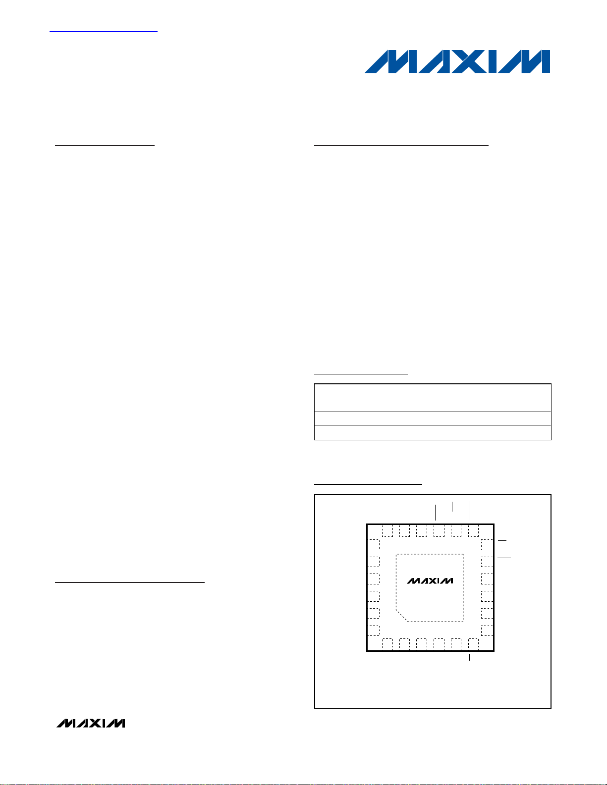
Pin Configurations
Ordering Information
19-3771; Rev 0; 7/05
For pricing, delivery, and ordering information, please contact Maxim/Dallas Direct! at
1-888-629-4642, or visit Maxim’s website at www.maxim-ic.com.
Ordering Information continued at end of data sheet.
+Denotes lead-free package.
Selector Guide appears at end of data sheet.
Pin Configurations continued at end of data sheet.
查询MAX6877供应商
PART TEMP RANGE
MAX6877ETG+ -40°C to +85°C 24 Thin QFN T2444-4
MAX6877ETG -40°C to +85°C 24 Thin QFN T2444-4
PINPACKAGE
PKG
CODE
TOP VIEW
GATE2
19
OUT1
20
GATE1
21
22
IN3
IN2
23
24
IN1
*EXPOSED PADDLE CONNECTED TO GND.
GATE3
OUT2
1718 16 14 13
+
12
CC
V
ABP
4mm x 4mm THIN QFN
OUT3
15
MAX6877
EP*
456
3
SET3
FAULT
SET2
PG/RST
SET1
MARGIN
12
11
10
9
8
7
EN/UV
TRK/SEQ
LTCH/RTR
TIMEOUT
SLEW
DELAY
GND
Page 2
MAX6877/MAX6878/MAX6879
Dual-/Triple-Voltage, Power-Supply
Trackers/Sequencers/Supervisors
2 _______________________________________________________________________________________
ABSOLUTE MAXIMUM RATINGS
ELECTRICAL CHARACTERISTICS
(VCC, IN1, IN2, or IN3 = +2.7V to +5.5V, EN/UV = MARGIN = ABP, TA= -40°C to +85°C, unless otherwise specified. Typical values
are at T
A
= +25°C, unless otherwise noted.) (Note 1)
Stresses beyond those listed under “Absolute Maximum Ratings” may cause permanent damage to the device. These are stress ratings only, and functional
operation of the device at these or any other conditions beyond those indicated in the operational sections of the specifications is not implied. Exposure to
absolute maximum rating conditions for extended periods may affect device reliability.
IN1, IN2, IN3, VCC....................................................-0.3V to +6V
ABP
.....................................-0.3V to the highest of V
IN1
- V
IN3
or V
CC
SET1, SET2, SET3 ....................................................-0.3V to +6V
GATE1, GATE2, GATE3 .........................................-0.3V to +12V
OUT1, OUT2, OUT3 .................................................-0.3V to +6V
LTCH/RTR, TRK/SEQ, MARGIN ...............................-0.3V to +6V
FAULT, PG/RST, EN/UV ...........................................-0.3V to +6V
DELAY, SLEW, TIMEOUT .........................................-0.3V to +6V
OUT_ Current....................................................................±50mA
GND Current.....................................................................±50mA
Input/Output Current (all pins except
OUT_ and GND) ...........................................................±20mA
Continuous Power Dissipation (T
A
= +70°C)
16-Pin 4mm x 4mm Thin QFN
(derate 16.9mW/°C above +70°C).............................1349mW
24-Pin 4mm x 4mm Thin QFN
(derate 20.8mW/°C above +70°C).............................1667mW
Operating Temperature Range ...........................-40°C to +85°C
Storage Temperature Range .............................-65°C to +150°C
Maximum Junction Temperature .....................................+150°C
Lead Temperature (soldering, 10s) .................................+300°C
(All voltages referenced to GND, unless otherwise noted.)
PARAMETER SYMBOL CONDITIONS MIN TYP MAX UNITS
Operating Voltage Range V
Supply Current I
SET_ Threshold Range V
SET_ Threshold Hysteresis V
SET_ Input Current I
EN/UV Input Voltage
EN/UV Input Current I
EN/UV Input Pulse Width t
DELAY, TIMEOUT Output Current I
DELAY, TIMEOUT Threshold
Voltage
SLEW Output Current (Note 4) I
Track/Sequence Slew-Rate
Timebase Accuracy
Timebase/C
S l ew - Rate Accur acy d ur i ng P ow er U p and P ow er - D ow n
Power-Good Threshold V
Ratio 100pF < C
SLEW
TH_HYS
V
V
CC
CC
TH
SET
EN_R
EN_F
EN
EN
D
S
SR C
TH_PG
Voltage on ABP (the highest of VCC or IN_)
to ensure that PG/RST and FAULT are valid
and GATE_ = 0V
Voltage on ABP (the highest of VCC or IN_)
to ensure the device is fully operational
V
= 5.5V , IN 1 = IN 2 = IN 3 = 3.3V , no l oad 1.1 1.8 mA
C C
SET_ falling, TA = +25oC 0.4925 0.5 0.5075
SET_ falling, TA = -40oC to +85oC 0.4875 0.5 0.5125
SET_ rising 0.5 %
SET_ = 0.5V -100 +100 nA
Input rising 1.286
Input falling 1.22 1.25 1.28
EN/UV falling, 100mV overdrive 7 µs
(Notes 2, 3) 2.12 2.5 2.88 µA
= 3.3V 1.25 V
V
C C
= 200pF (Note 4) -15 +15 %
SLEW
C
= 200pF, ABP = 5.5V (Note 4) -50 +50 %
SLEW
V
falling 91.5 92.5 93.5 %
OUT_
< 1nF (Note 4) 104 kΩ
SLEW
1.4
2.7 5.5
-5 +5 µA
22.5 25 27.5 µA
V
V
V
Page 3
MAX6877/MAX6878/MAX6879
Dual-/Triple-Voltage, Power-Supply
Trackers/Sequencers/Supervisors
_______________________________________________________________________________________ 3
Note 1: Specifications guaranteed for the stated global conditions. 100% production tested at TA= +25°C and TA= +85°C.
Specifications at T
A
= -40°C to +85°C are guaranteed by design. These devices meet the parameters specified when at
least one of V
CC
, IN1/IN2/IN3 is between 2.7V to 5.5V, while the remaining IN1/IN2/IN3 are between 0 and 5.5V.
Note 2: A current I
D
= 2.5µA ±15% is generated internally and is used to set the DELAY and TIMEOUT periods and used as a refer-
ence for t
DELAY
and t
TIMEOUT
.
Note 3: The total DELAY is t
DELAY
= 200ms + (500kΩ x C
DELAY
). Leave DELAY unconnected for 200µs delay. The total TIMEOUT is
t
TIMEOUT
= 200µs + (500kΩ x C
TIMEOUT
). Leave TIMEOUT unconnected for 200µs timeout.
Note 4: A current I
S
= 25µA ±10% is generated internally and used as a reference for t
FAULT
, t
RETRY
, and slew rate.
Note 5: During power-up, only the condition OUT_ < ramp - V
TRK
is checked in order to stop the ramp. However, both conditions
OUT_ < ramp - V
TRK_F
and OUT_ > ramp + V
TRK_F
cause a fault. During power-down, only the condition OUT > ramp +
V
TRK
is checked in order to stop the ramp. However, both conditions OUT_ < ramp - V
TRK_F
and OUT_ > ramp + V
TRK_F
cause a fault (see Figure 10). Therefore, if OUT1, OUT2, and OUT3 (during power-up tracking and power-down) differ by
more than 2 x V
TRK_F
, a fault condition is asserted.
Note 6: A 100Ω pulldown to GND activated by a fault condition. See the Internal Pulldown section.
ELECTRICAL CHARACTERISTICS (continued)
(VCC, IN1, IN2, or IN3 = +2.7V to +5.5V, EN/UV = MARGIN = ABP, TA= -40°C to +85°C, unless otherwise specified. Typical values
are at T
A
= +25°C, unless otherwise noted.) (Note 1)
PARAMETER SYMBOL CONDITIONS MIN TYP MAX UNITS
Power-Good Threshold Hysteresis V
GATE_ Output High V
GATE_ Pullup Current I
HYS_PGVOUT_
GOH
GUP
I
GD
GATE_ Pulldown Current
I
GDS
SET_ to GATE_ Delay t
FAULT, PG/RST Output Low V
Tracking Differential Voltage Stop
Ramp
Tracking Differential Fault Voltage V
D-GATE
OL
V
TRK
TRK_F
Tracking Differential Voltage
Hysteresis
Power-Low Threshold V
Power-Low Hysteresis V
TH_PL
TH_PLHYS
OUT to GND Pulldown Impedance V
MARGIN, TRK/SEQ, LTCH/RTR
Pullup Current
MARGIN, TRK/SEQ, LTCH/RTR
Input Voltage
I
IN
V
IL
V
IH
MARGIN, TRK/SEQ, LTCH/RTR
Glitch Rejection
rising 0.5 %
I
SOURCE
= 0.5µA
During power-up and power-down,
V
= 1V
GATE_
During power-up and power-down,
V
= 5V
GATE_
When disabled, V
When disabled, V
GATE_
GATE_
= 5V, V
= 5V, V
IN_
IN_
IN_ +
4.2
2.5 4 µA
2.5 4 µA
≥ 2.7V 9.5
≥ 4V 20
IN_ +
5.0
IN_ +
5.8
V
mA
SET falling, 25mV overdrive 6 µs
V
IN_
V
IN_
≥ 2.7V, I
≥ 4.0V, I
= 1mA, output asserted 0.3
SINK
= 4mA, output asserted 0.4
SINK
V
Differential between each of the OUT_ and
the ramp voltage during power-up and
75 125 180 mV
power-down, Figure 10 (Note 5)
Differential between each of the OUT_ and
the ramp voltage, Figure 10 (Note 5)
200 250 310 mV
20 %
OUT_ falling 125 142 170 mV
OUT_ rising 10 mV
> 2.7V (Note 6) 100 Ω
ABP
71013µA
0.8
2.0
V
100 ns
Page 4
MAX6877/MAX6878/MAX6879
Dual-/Triple-Voltage, Power-Supply
Trackers/Sequencers/Supervisors
4 _______________________________________________________________________________________
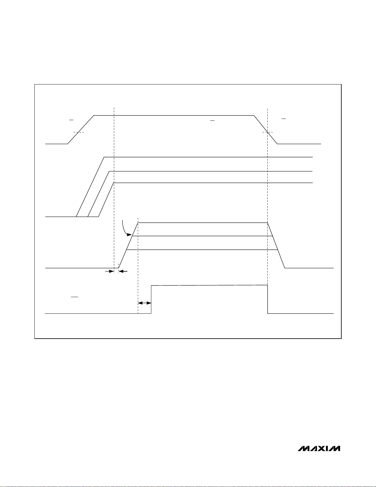
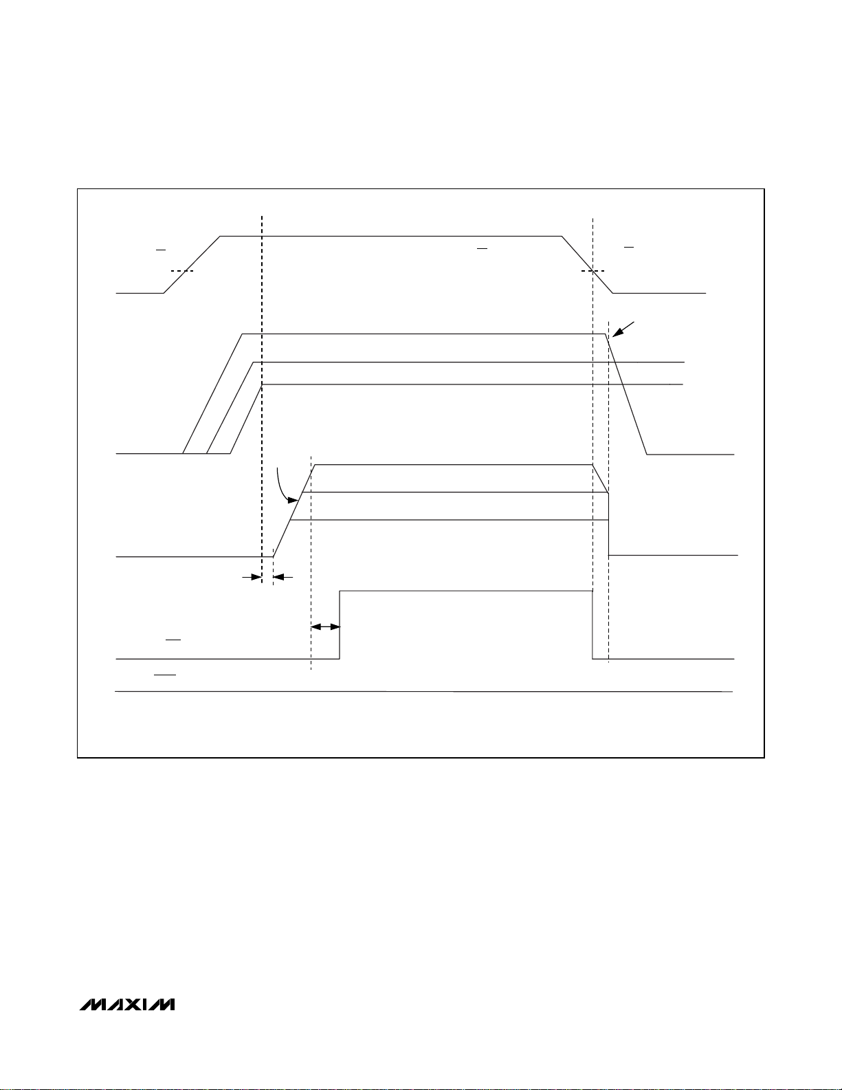
Figure 1. Tracking Timing Diagram in Normal Mode
EN/UV
V
EN_R
IN_
OUT_
EN/UV
IN1 = 2.5V
IN2 = 1.8V
IN3 = 0.7V
CAPACITORADJUSTED
SLEW RATE
t
DELAY
BUS VOLTAGE MONITORED THROUGH EN/UV INPUT
MONITORED THROUGH SET THRESHOLDS ON SET_ INPUTS
OUT1 = 2.5V
OUT2 = 1.8V
OUT3 = 0.7V
EN/UV
V
EN_F
PG/RST
t
TIMEOUT
Page 5
MAX6877/MAX6878/MAX6879
Dual-/Triple-Voltage, Power-Supply
Trackers/Sequencers/Supervisors
_______________________________________________________________________________________ 5
Figure 2. Tracking in Fast Shutdown Mode
EN/UV
V
EN_R
PG/RST
IN_
OUT_
IN1 = 2.5V
IN2 = 1.8V
IN3 = 0.7V
CAPACITORADJUSTED
SLEW RATE
t
DELAY
t
TIMEOUT
BUS VOLTAGE MONITORED THROUGH EN/UV INPUT
MONITORED THROUGH SET THRESHOLDS ON SET_ INPUTS
OUT1 = 2.5V
OUT2 = 1.8V
OUT3 = 0.7V
EN/UV
V
EN_F
IN1 GOES BELOW
SET1 THRESHOLD
FAULT = HIGH
FORCED INTO QUICK SHUTDOWN AFTER NORMAL SHUTDOWN WHEN IN1 GOES BELOW ITS SET VOLTAGE
Page 6
MAX6877/MAX6878/MAX6879
Dual-/Triple-Voltage, Power-Supply
Trackers/Sequencers/Supervisors
6 _______________________________________________________________________________________
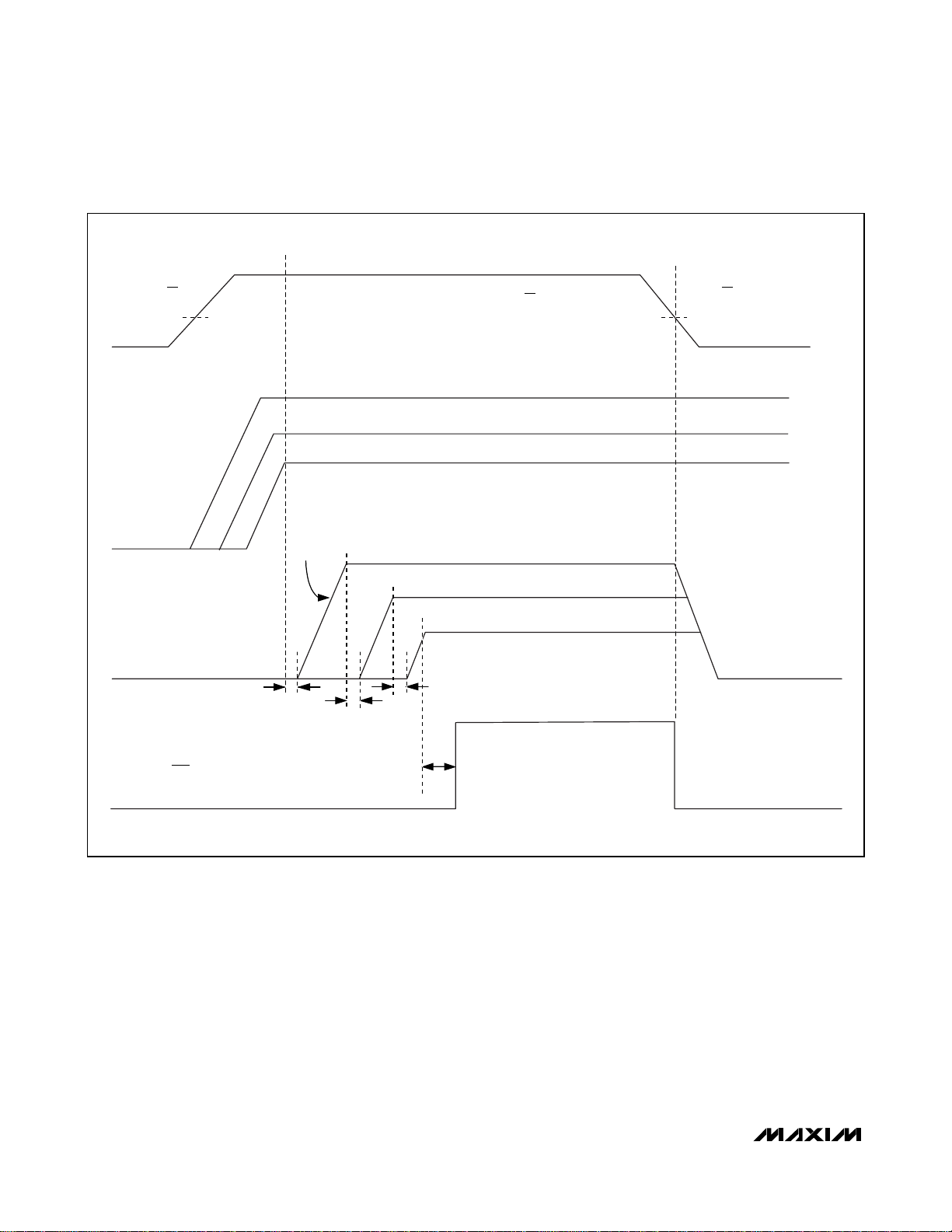
Figure 3. Sequencing in Normal Mode
EN/UV
V
EN_R
IN1 = 2.5V
IN2 = 1.8V
IN_
OUT_
IN3 = 0.7V
CAPACITORADJUSTED
SLEW RATE
t
DELAY
BUS VOLTAGE MONITORED THROUGH EN/UV INPUT
MONITORED THROUGH SET THRESHOLDS ON SET_ INPUTS
OUT1 = 2.5V
OUT2 = 1.8V
OUT3 = 0.7V
t
t
DELAY
DELAY
EN/UV
V
EN_F
t
PG/RST
TIMEOUT
Page 7
MAX6877/MAX6878/MAX6879
Dual-/Triple-Voltage, Power-Supply
Trackers/Sequencers/Supervisors
_______________________________________________________________________________________ 7
V
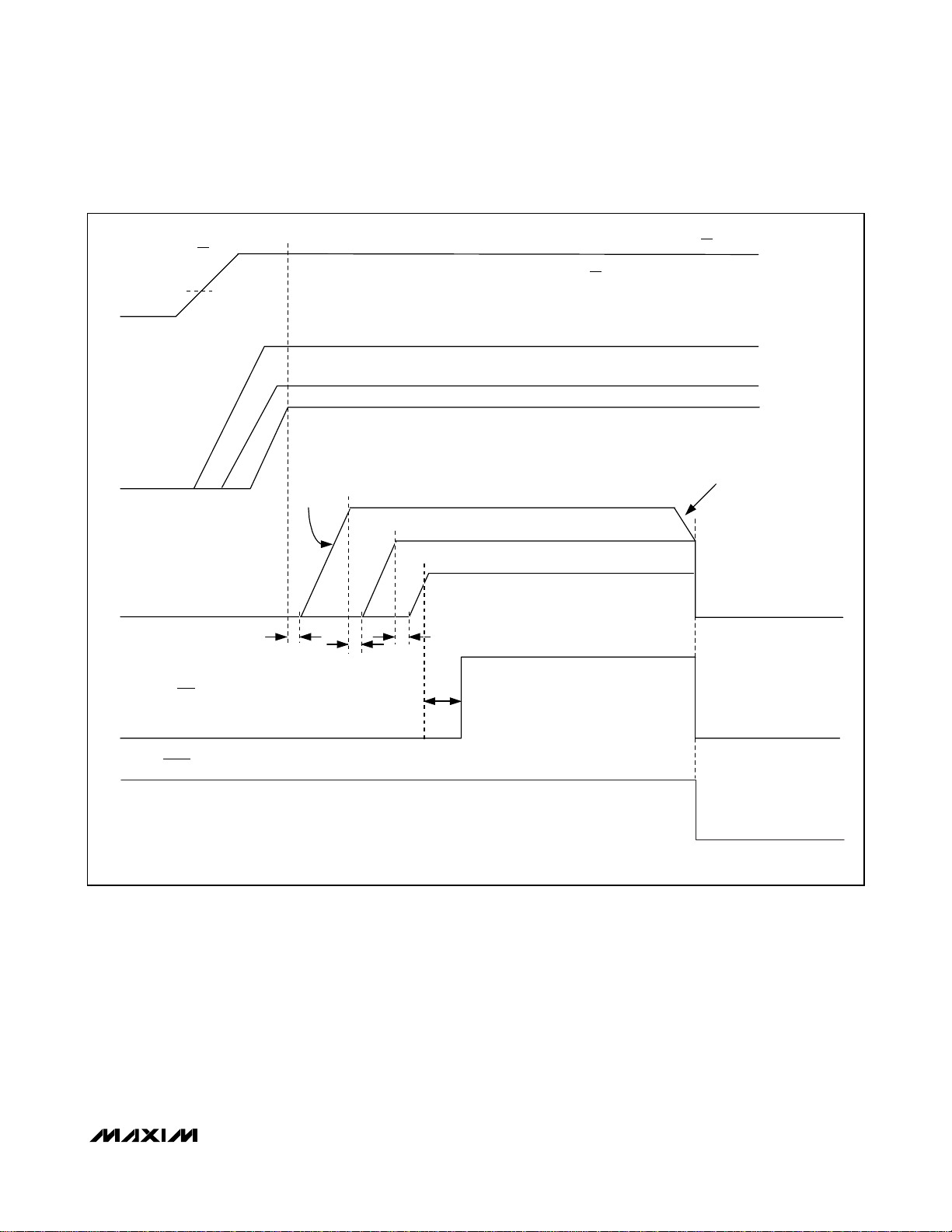
Figure 4. Sequencing in Fast Shutdown Mode
EN_R
IN_
EN/UV
EN/UV
BUS VOLTAGE MONITORED THROUGH EN/UV INPUT
IN1 = 2.5V
IN2 = 1.8V
IN3 = 0.7V
MONITORED THROUGH SET THRESHOLDS ON SET_ INPUTS
CAPACITORADJUSTED
SLEW RATE
OUT_
t
DELAY
PG/RST
FAULT
FORCED INTO QUICK SHUTDOWN WHEN OUT1 FALLS BELOW 92.5% of IN1
t
DELAY
OUT1 = 3.3V
t
DELAY
t
TIMEOUT
OUT2 = 1.8V
OUT3 = 0.7V
OUT_ FORCED
BELOW V
TH_PG
Page 8
MAX6877/MAX6878/MAX6879
Dual-/Triple-Voltage, Power-Supply
Trackers/Sequencers/Supervisors
8 _______________________________________________________________________________________
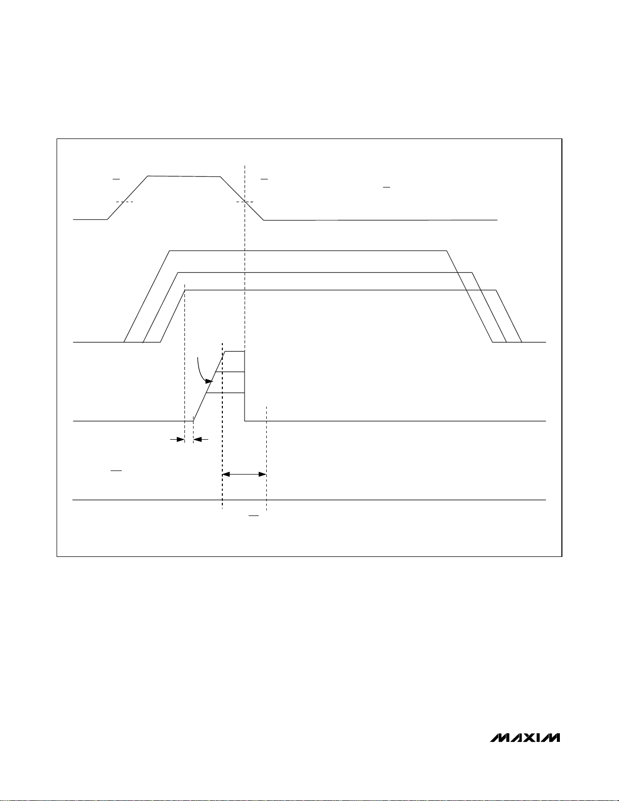
Figure 5. Timing Diagram (Aborted Tracking)
EN/UV
V
EN_R
IN1 = 2.5V
IN2 = 1.8V
IN3 = 0.7V
IN_
CAPACITORADJUSTED
SLEW RATE
OUT_
t
PG/RST = LOW
DELAY
EN/UV
BUS VOLTAGE MONITORED THROUGH EN/UV INPUT
V
EN_F
MONITORED THROUGH SET THRESHOLDS ON SET_ INPUTS
OUT1 = 2.5V
OUT2 = 1.8V
OUT3 = 0.7V
*t
TIMEOUT
*ANY POWER-DOWN CONDITION BEFORE t
(PG/RST ASSERTED) CAUSES A SHUTDOWN.
TIMEOUT
Page 9

MAX6877/MAX6878/MAX6879
Dual-/Triple-Voltage, Power-Supply
Trackers/Sequencers/Supervisors
_______________________________________________________________________________________ 9
Figure 6. Timing Diagram (Aborted Sequencing)
EN/UV EN/UV
V
EN_R
IN_
OUT_
BUS VOLTAGE MONITORED
THROUGH EN/UV INPUT
IN1 = 2.5V
IN2 = 1.8V
IN3 = 0.7V
CAPACITORADJUSTED
SLEW RATE
OUT1 = 2.5V
t
DELAY
t
DELAY
t
DELAY
*t
TIMEOUT
OUT2 = 1.8V
V
EN_F
MONITORED THROUGH SET THRESHOLDS ON SET_ INPUTS
OUT3 = 0.7V
PG/RST = LOW
*ANY POWER-DOWN CONDITION BEFORE t
TIMEOUT
(PG/RST ASSERTED) CAUSES A SHUTDOWN.
Page 10

MAX6877/MAX6878/MAX6879
Dual-/Triple-Voltage, Power-Supply
Trackers/Sequencers/Supervisors
10 ______________________________________________________________________________________
Figure 8. t
FAULT
and t
RETRY
Timing Diagram in Sequencing
Figure 7. t
FAULT
and t
RETRY
Timing Diagram in Tracking
EN/UV
V
EN_R
OUT2 AND OUT3 ARE WAITING
OUT_
FAULT
EN/UV
t
DELAY
t
AND t
FAULT
ALL SET_ > 0.5V AND V
RETRY
OUT1 IS SLOW
NOT TO SCALE
OR IN_ ≥ 2.7V
CC
t
FAULT
125mV
t
RETRY
t
DELAY
OUT1
OUT_
OUT2
OUT3 IS SLOW
OUT2 AND OUT3 ARE WAITING
OUT1 IS SLOW
t
FAULT
OUT1
OUT2
OUT3 IS SLOW
t
DELAY
t
DELAY
t
DELAY
FAULT
t
FAULT
ALL SET_ > 0.5V AND V
t
DELAY
AND t
NOT TO SCALE
RETRY
t
DELAY
t
DELAY
OR IN_ ≥ 2.7V
CC
t
FAULT
t
RETRY
t
FAULT
Page 11

MAX6877/MAX6878/MAX6879
Dual-/Triple-Voltage, Power-Supply
Trackers/Sequencers/Supervisors
______________________________________________________________________________________ 11
Typical Operating Characteristics
(V
CC_
= 2.7V to 5.5V, C
SLEW
= 200pF, EN = MARGIN = ABP, TA= +25°C, unless otherwise noted.)
VCC SUPPLY CURRENT
vs. INPUT VOLTAGE
1.4
1.3
1.2
1.1
1.0
SUPPLY CURRENT (mA)
CC
V
0.9
0.8
TA = +25°C
TA = -40°C
2.5 5.5
INPUT VOLTAGE (V)
NORMALIZED SET_ THRESHOLD
vs. TEMPERATURE
1.005
1.004
1.003
1.002
1.001
1.000
0.999
0.998
NORMALIZED SET_ THRESHOLD
0.997
0.996
0.995
-40 85
TEMPERATURE (°C)
DELAY TIMEOUT
vs. C
C
DELAY
DELAY
(µF)
1000
100
10
DELAY TIMEOUT (ms)
1
0.1
0.0001 1
NORMALIZED POWER-GOOD TIMEOUT
TA = +85°C
603510-15
0.10.010.001
1.15
1.10
MAX6877 toc01
1.05
1.00
0.95
0.90
0.85
NORMALIZED POWER-GOOD TIMEOUT
0.80
0.75
5.04.54.03.53.0
-40 85
TEMPERATURE (°C)
6035-15 10
NORMALIZED DELAY TIMEOUT
vs. TEMPERATURE
vs. TEMPERATURE
1.25
1.20
MAX6877 toc04
1.15
1.10
1.05
1.00
0.95
0.90
NORMALIZED DELAY TIMEOUT
0.85
0.80
0.75
-40 85
TEMPERATURE (°C)
603510-15
NORMALIZED EN/UV THRESHOLD
vs. TEMPERATURE
1.005
1.004
MAX6877 toc07
1.003
1.002
1.001
1.000
0.999
0.998
0.997
NORMALIZED EN_/UV THRESHOLD
0.996
0.995
-40 85
TEMPERATURE (°C)
603510-15
1000
MAX6877 toc02
100
10
1
POWER-GOOD TIMEOUT (ms)
0.1
0.0001 1
10,000
MAX6877 toc05
1000
SLEW RATE (V/s)
100
10
30
27
MAX6877 toc08
24
21
18
15
12
9
IN_ TRANSIENT DURATION (µs)
6
3
0
POWER-GOOD TIMEOUT
vs. C
TIMEOUT
MAX6877 toc03
0.10.010.001
C
(µF)
TIMEOUT
SLEW RATE
vs. C
SLEW
MAX6877 toc06
10 10,000
IN_ = 3.3V
0300
100 1000
C
(pF)
SLEW
IN_ TRANSIENT DURATION
vs. IN_ THRESHOLD OVERDRIVE
PG/RST GOES LOW ABOVE THE CURVE
25020015010050
IN_ THRESHOLD OVERDRIVE (mV)
MAX6877 toc09
Page 12

MAX6877/MAX6878/MAX6879
Dual-/Triple-Voltage, Power-Supply
Trackers/Sequencers/Supervisors
12 ______________________________________________________________________________________
Typical Operating Characteristics (continued)
(V
CC_
= 2.7V to 5.5V, C
SLEW
= 200pF, EN = MARGIN = ABP, TA= +25°C, unless otherwise noted.)
GATE_ VOLTAGE LOW
vs. GATE SINK CURRENT
MAX6877 toc10
GATE SINK CURRENT (mA)
GATE_ VOLTAGE LOW (V)
981 2 3 5 64 7
0.2
0.4
0.6
0.8
1.0
1.2
1.4
1.6
0
010
FAST SHUTDOWN WITH RETRY
MAX6877 toc15
100ms/div
FAULT
1V/div
OUT2
2V/div
OUT1
2V/div
OUT3
2V/div
THRESHOLD ERROR
AT OUT1,
OUT1 PULLED BELOW
92.5% OF IN1
GATE_ OUTPUT VOLTAGE HIGH
vs. GATE SOURCE CURRENT
10
9
8
7
6
5
4
3
GATE_ VOLTAGE HIGH (V)
2
1
0
03.0
GATE SOURCE CURRENT (µA)
2.52.01.51.00.5
MAX6877 toc11
TRACKING MODE
10ms/div
MAX6877 toc12
EN/UV
2V/div
OUT1
OUT2
1V/div
OUT3
SEQUENCING MODE
20ms/div
MAX6877 toc13
EN/UV
2V/div
OUT1
OUT2
1V/div
OUT3
FAST SHUTDOWN
40ms/div
MAX6877 toc14
EN/UV
2V/div
OUT1
OUT2
1V/div
OUT3
FAULT
2V/div
Page 13

MAX6877/MAX6878/MAX6879
Dual-/Triple-Voltage, Power-Supply
Trackers/Sequencers/Supervisors
______________________________________________________________________________________ 13
Pin Description
PIN
MAX6877
NAME FUNCTION
11—V
CC
Optional Supply Voltage Input. Connect VCC to an alternate (i.e., always-on)
supply if desired. Leave V
CC
unconnected, if not used. VCC allows IN_
supplies less than UVLO to be tracked. V
CC
is internally pulled down by a
100kΩ resistor.
221ABP
Internal Supply Bypass Input. Bypass ABP with a 1µF capacitor to GND. ABP
maintains the device supply voltage during rapid power-down conditions.
3 — — SET3
4 4 2 SET2
5 5 3 SET1
Externally Adjusted IN_ Undervoltage Lockout Threshold. Connect SET_ to
an external resistor-divider network to set the desired undervoltage threshold
for each IN_ supply (see the Typical Application Circuit). All SET_ inputs
must be above the internal SET_ threshold (0.5V) to enable tracking or
sequencing functionality.
—
3, 16, 17,
22
— N.C. No Connection. Not internally connected.
664EN/UV
Logic-Enable Input or Undervoltage Lockout Monitor Input. EN/UV must be
high (EN/UV > V
EN_R
) to enable voltage tracking or sequencing power-up
operation. OUT_ begins tracking down when EN/UV < V
EN_F
. Connect EN/UV
to an external resistor-divider network to set the external UVLO threshold.
7 7 5 GND Ground
8 8 6 DELAY
Tracking Startup/Sequence Delay Select Input. Connect a capacitor from
DELAY to GND to select the desired delay period before tracking is enabled
(after all SET_ inputs and EN/UV are above their respective thresholds) or
between supply sequences. Leave DELAY unconnected for the default
200µs delay period.
9 9 7 SLEW
Slew-Rate Adjustment Input. Connect a capacitor from SLEW to GND to
select the desired OUT_ slew rate.
10 10 —
PG/RST Timeout Period Adjust Input. PG/RST asserts high after the timeout
period when all OUT_ exceed their IN_ referenced threshold. Connect a
capacitor from TIMEOUT to GND to set the desired timeout period. Leave
TIMEOUT unconnected for the default 200µs delay period.
11 11 8
Latch/Autor etr y S el ecti on Inp ut. D r i ve L TC H/RTR l ow to sel ect the l atch m od e.
C onnect L TC H/RTR to ABP or l eave unconnected to sel ect autor etr y m od e.
L TC H/RTR i s i nter nal l y p ul l ed up to ABP thr oug h a 10µA cur r ent sour ce.
12 12 9
Track/Sequence Select Input. Drive TRK/SEQ low to enable supply tracking
function. Connect TRK/SEQ to ABP or leave it unconnected to enable supply
sequencing. TRK/SEQ is internally pulled to ABP through a 10µA current
source.
13 13 — MARGIN
Margin Input, Active-Low. Drive MARGIN low to enable margin mode (see
the Margin section). The MARGIN functionality is disabled (returns to normal
monitoring mode) after MARGIN returns high. MARGIN is internally pulled up
to ABP through a 10µA current source.
MAX6878 MAX6879
TIMEOUT
LTCH/RTR
TRK/SEQ
Page 14

MAX6877/MAX6878/MAX6879
Dual-/Triple-Voltage, Power-Supply
Trackers/Sequencers/Supervisors
14 ______________________________________________________________________________________
Pin Description (continued)
PIN
MAX6877
NAME FUNCTION
14 14 — PG/RST
Power-Good Output, Open-Drain. PG_RST asserts high t
TIMEOUT
after all
OUT_ voltages exceed the V
TH_PG
thresholds.
15 15 10
FAULT
Tracking Fault Alert Output, Active Low, Open-Drain. FAULT asserts low if a
tracking failure is present for longer than the selected fault period or if
tracking voltages fail by more than ±250mV. FAULT asserts low if any OUT_
falls below the corresponding IN_ voltage.
16 — — OUT3
Channel 3 Monitored Output Voltage. Connect OUT3 to the source of an nchannel FET. A fault condition activates a 100Ω pulldown to ground.
17 — — GATE3
Gate Drive for External n-Channel FET. An internal charge pump boosts
GATE3 to V
IN3
+ 5V to fully enhance the external n-channel FET when power-
up is complete.
18 18 11 OUT2
Channel 2 Monitored Output Voltage. Connect OUT2 to the source of an
n-channel FET. A fault condition activates a 100Ω pulldown to ground.
19 19 12 GATE2
Gate Drive for External n-Channel FET. An internal charge pump boosts
GATE2 to V
IN2
+ 5V to fully enhance the external n-channel FET when power-
up is complete.
20 20 13 OUT1
Channel 1 Monitored Output Voltage. Connect OUT1 to the source of an
n-channel FET. A fault condition activates a 100Ω pulldown to ground.
21 21 14 GATE1
Gate Drive for External n-Channel FET. An internal charge pump boosts
GATE1 to V
IN1
+ 5V to fully enhance the external n-channel FET when power-
up is complete.
22 — — IN3
23 23 15 IN2
24 24 16 IN1
Supply Input Voltage. IN1, IN2, or IN3 must be greater than the internal
undervoltage lockout (V
ABP
= 2.7V) to enable the tracking or sequencing
functionality. Each IN_ input is simultaneously monitored by SET_ inputs to
ensure all supplies have stabilized before power-up is enabled. If IN_ is
connected to ground or left unconnected and SET_ is above 0.5V, then nosequencing control is performed on that channel. Each IN_ is internally
pulled down by a 100kΩ resistor.
EP EP EP EP Exposed Paddle. Connect exposed paddle to ground.
MAX6878 MAX6879
Page 15

MAX6877/MAX6878/MAX6879
Dual-/Triple-Voltage, Power-Supply
Trackers/Sequencers/Supervisors
______________________________________________________________________________________ 15
Functional Diagram
IN1
V
CC
IN1
MAX6877
SET1
IN2
SET2
IN3
SET3
V
BUS
EN/UVLO
MARGIN
COMP
COMP
COMP
COMP
V
REF
IN2
INTERNAL
/UVLO
V
CC
CONTROL
LOGIC
IN3
ABP
RAMP
GENERATOR
TRACKING
MONITORS
OUT1
OUT2
OUT3
IN1
IN2
IN3
GATE1
IN1
CHARGE
PUMP
GATE
CONTROLLER
IN2 TO OUT2
CONTROL BLOCK
IN3 TO OUT3
CONTROL BLOCK
PG CIRCUIT
TO LOAD
OUT1
GATE2
OUT2
GATE3
OUT3
GND
DELAY
LTCH/RTR
FAULT
TRK/SEQ
SLEW
C
SLEW
TIMEOUT
C
TIMEOUT
PG/RST
Page 16

MAX6877/MAX6878/MAX6879
Dual-/Triple-Voltage, Power-Supply
Trackers/Sequencers/Supervisors
16 ______________________________________________________________________________________
Detailed Description
The MAX6877/MAX6878/MAX6879 multivoltage power
trackers/sequencers/supervisors monitor up to three
system voltages and provide proper power-up and
power-down control for systems requiring voltage
tracking or sequencing. These devices ensure controlled voltage tracking with a specified range or
sequencing in the proper order as system power supplies are enabled. The MAX6877/MAX6878/MAX6879
generate all required voltages and timing to control up
to three external n-channel pass FETs for the
OUT1/OUT2/OUT3 supply voltages (see the Selector
Guide for different features of each device.)
The MAX6877/MAX6878/MAX6879 feature adjustable
undervoltage thresholds for each input supply. When
all the voltages are above these adjusted thresholds,
the devices turn on the external n-channel MOSFETs to
either sequence or track the voltages to the system.
During the voltage-tracking mode, the voltage at the
GATE of each MOSFET is increased to slowly bring up
all supplies at a controlled slew rate. The voltage at the
source (output) of each MOSFET is internally compared
to a control ramp to maintain a low differential between
each monitored supply. Tracking is dynamically adjusted to force all outputs to track within 125mV of the reference ramp. If for any reason any supplies fail to track
within ±250mV of the reference ramp, the FAULT out-
put is asserted, the power-up mode is terminated, and
all outputs are quickly powered off. In sequencing
mode, the outputs are turned on one after the other,
OUT1 first and OUT3 last. The MAX6877/MAX6878/
MAX6879 feature an autoretry or latch-off mode with
capacitor-adjusted timing.
These devices also provide a controlled power-down
(tracking mode) when the system shuts off in an orderly
manner. When an unexpected fault occurs, the outputs
are all pulled down simultaneously with an internal
100Ω pulldown to help discharge capacitive loads at
the MOSFET’s source.
The MAX6877/MAX6878/MAX6879 feature independent
internal charge pumps to fully enhance the external
FETs for low-voltage drops at highpass currents. The
MAX6877/MAX6878 also feature a power-good output
with a selectable timeout period that can be used for
system reset.
The MAX6877/MAX6878/MAX6879 monitor up to three
voltages. Devices may be configured to exclude any
IN_. To disable the tracking or sequencing operation of
any IN_, connect the IN_ to ground (or leave unconnected) and connect SET_ to a voltage greater than
0.5V. The channel exclusion feature adds more flexibili-
ty to the device in a variety of different applications. As
an example, the MAX6877 can track or sequence two
voltages using IN1 and IN2 while IN3 is left disabled.
Powering the
MAX6877/MAX6878/MAX6879
These devices derive power from either the IN1, IN2, or
IN3 voltage inputs or VCC(see the Functional Diagram).
VCCor one of the IN_ inputs must be at least +2.7V to
ensure full device operation.
The highest input voltage on IN1/IN2/IN3 or VCCsupplies power to the devices. Internal hysteresis ensures
that the supply input that initially powers these devices
continues to power the MAX6877/MAX6878/MAX6879
when multiple input voltages are within 100mV (typ) of
each other.
ABP
ABP powers the analog circuitry. Bypass ABP to GND
with a 1µF ceramic capacitor installed as close to the
device as possible. ABP takes the highest voltage of
IN_ or VCC. Do not use ABP to provide power to external circuitry. ABP maintains the device supply voltage
during rapid power-down conditions.
Tracking and Sequencing Modes
(
TRK
/SEQ)
To enable the power-up/power-down voltage-tracking
operation, drive TRK/SEQ low (connect TRK/SEQ to
GND). To enable power-up sequencing and powerdown tracking functions, drive TRK/SEQ high (connect
TRK/SEQ to ABP) or leave it unconnected. TRK/SEQ is
internally pulled to ABP through a 10µA current source
(see Figures 1 and 3).
Tracking
To operate in tracking mode, connect TRK/SEQ to
GND. When V
EN/UV
> 1.25V and all SET_ inputs are
above the internal SET_ threshold (0.5V), the tracking
process is initiated. The MAX6877/MAX6878/MAX6879
generate an internal reference ramp voltage that drives
the control loops for the tracked voltages. The tracking
functionality is monitored with a comparator control
block for each output (see the Functional Diagram).
The comparators monitor each OUT_ voltage with
respect to the common reference ramp voltage to
ensure the OUT_ voltages stay within 125mV of the reference ramp, monitor each tracked output voltage with
respect to its source input voltage, and monitor each
output voltage with respect to GND during powerup/retry cycles. If for any reason any supplies fail to
track within ±250mV of the reference ramp, the FAULT
output is asserted, the power-up mode is terminated,
and all outputs are quickly powered off.
Page 17

MAX6877/MAX6878/MAX6879
Dual-/Triple-Voltage, Power-Supply
Trackers/Sequencers/Supervisors
______________________________________________________________________________________ 17
During ramp up, if an OUT_ voltage is less than the reference ramp voltage by more than 125mV, the control
loop dynamically stops the control ramp voltage from
rising until the slow OUT_ voltage catches up. If an
OUT_ voltage is greater or less than the reference ramp
voltage by more than 250mV, a fault is signaled and a
power-down phase is initiated.
The slew rate for the reference ramp voltage is capacitor adjustable. Connect a capacitor from SLEW to
ground to select the desired OUT_ slew rate. When all
OUT_ voltages have exceeded the V
TH_PG
percentage
of the IN_ voltage (external n-channel FET is saturated),
PG/RST asserts high after t
TIMEOUT
indicating success-
ful tracking.
Sequencing
The sequencing operation can be initiated after all
input conditions for power-up are met V
EN/UV
> 1.25V
and all SET_ inputs are above the internal SET_ threshold (0.5V). In sequencing mode, the outputs are turned
on sequentially, OUT1 first and OUT3 last. Before turning on each channel, a delay period occurs as in
Figure 3 (programmable by connecting a capacitor
from DELAY to ground). The power-up phase for each
channel ends when its output voltage exceeds a fixed
percentage (V
TH_PG
) of the corresponding IN_ voltage.
When all channels have exceeded these thresholds,
PG/RST asserts high after t
TIMEOUT
, indicating a suc-
cessful sequence.
If there is a fault condition during the initial power-up
sequence, the process is aborted.
When powering down, all outputs turn off simultaneously, tracking each other. No reverse power-down
sequencing occurs.
Power-Up and Power-Down
During power-up, the OUT_ is forced to follow the internal
reference ramp voltage by an internal loop that controls
the GATE_ of the external MOSFET. This phase must be
completed within the adjustable fault timeout period; otherwise, the part forces a shutdown on all GATE_.
Once the power-up is completed, a power-down phase
can be initiated by forcing V
EN/UV
below V
EN_F
. The
reference voltage ramp ramps down at the capacitoradjusted slew rate. The control-loop comparators monitor each OUT_ voltage with respect to the common
reference ramp voltage. During ramp down, if an OUT_
voltage is greater than the reference ramp voltage by
more than V
TRK
, the control loop dynamically stops the
control ramp voltage from decreasing until the slow
OUT_ voltage catches up. If an OUT_ voltage is greater
or less than the reference ramp voltage by more than
V
TRK_F
, a fault is signaled and the fast-shutdown mode
is initiated. In fast-shutdown mode, a 100Ω pulldown
resistor is connected from OUT_ to GND to quickly discharge capacitance at OUT_ and GATE _ is pulled low
with a strong I
GDS
current (see Figures 2 and 4).
Figures 5 and 6 show aborted tracking and sequencing
modes. When EN/UV goes low before t
TIMEOUT
expires, all the outputs go low and the device goes into
fast shutdown.
Internal Pulldown
To ensure that the OUT_ voltages are not held high by
a large output capacitance after a fault has occurred,
there is a 100Ω internal pulldown at OUT_. The pulldown ensures that all OUT_ voltages are below V
TH_PL
(referenced to GND) before power-up cycling is initiated. The internal pulldown also ensures a fast discharge
of the output capacitor during fast shutdown and fault
modes. The pulldowns are not present during normal
operation.
Stability Comment
No external compensation is required for tracking or
slew-rate control.
Inputs
IN1/IN2/IN3
The highest voltage on VCC, IN1, IN2, or IN3 supplies
power to the device. The undervoltage threshold for
each IN_ supply is set with an external resistor-divider
from each IN_ to SET_ to ground.
Undervoltage Lockout Threshold Inputs (SET_)
The MAX6877 features three and the MAX6878/
MAX6879 feature two externally adjustable IN_ undervoltage lockout (UVLO) thresholds (SET1, SET2, SET3) to
enable sequencing/tracking functionality. The undervoltage threshold for each IN_ supply is set with an external resistor-divider from each IN_ to SET_ to ground
(see Figure 9). All SET_ inputs must be above the internal SET_ threshold (0.5V) to enable tracking/sequencing functionality. Use the following formula to set the
UVLO threshold:
V
IN_
= VTH(R1 + R2) / R2
where V
IN_
is the undervoltage lockout threshold and
V
TH
is the 500mV SET threshold.
Margin Input (
MMAARRGGIINN
)
MARGIN allows system-level testing while power supplies are below the normal ranges as adjusted by the
SET_ inputs. Drive MARGIN low before varying system
Page 18

MAX6877/MAX6878/MAX6879
Dual-/Triple-Voltage, Power-Supply
Trackers/Sequencers/Supervisors
18 ______________________________________________________________________________________
voltages below the adjusted thresholds to avoid signaling an error. The state of PG/RST and FAULT outputs
does not change while MARGIN is low. PG/RST,
FAULT, and all monitoring functions are disabled while
MARGIN is low. MARGIN makes it possible to vary the
supplies without a need to adjust the thresholds to prevent tracker/sequencer alerts or faults. Drive MARGIN
high or leave it unconnected for normal operating
mode.
Slew-Rate Control Input (SLEW)
The reference ramp voltage slew rate during any controlled power-up/down phase can be programmed in
the 90V/s to 950V/s range by connecting a capacitor
(C
SLEW
) from SLEW to ground. Use the following for-
mula to calculate the typical slew rate:
Slew Rate = (9.35 x 10⁻⁸)/ C
SLEW
where slew rate is in V/s and C
SLEW
is in farads.
The capacitor at C
SLEW
also sets the FAULT timeout
period (t
FAULT
) and FAULT retry timeout period
(t
RETRY
) (see Table 1).
For example, if C
SLEW
= 100pF, we have t
RETRY
=
350ms, t
FAULT
= 21.91ms, slew rate = 935V/s. For
example, if C
SLEW
= 1nF, we have t
RETRY
= 3.5s,
t
FAULT
= 219ms, slew rate = 93.5V/s.
C
SLEW
is the capacitor on the SLEW pad, and must be
large enough to make the parasitic capacitance negligible. C
SLEW
should be in the range of 100pF <
C
SLEW
< 1nF.
Limiting Inrush Current
The capacitor connected at SLEW controls the OUT_S
slew rate, thus controlling the inrush current required to
charge the load capacitor at the outputs (OUT_). Using
the programmed slew rate, limit the inrush current by
using the following formula:
I
INRUSH
= C
OUT
x SR
where I
INRUSH
is in amperes, C
OUT
is in farads, and SR
is in V/s.
Delay Time Input (DELAY)
To adjust the desired delay period (t
DELAY
) before
tracking/sequencing is enabled, connect a capacitor
(C
DELAY
) between DELAY to ground (see Figures 1 to 8).
The selected delay time is also enforced when EN/UV
rises from low to high when all the input voltages
(IN1/IN2/IN3) are present. Use the following formula to
calculate the delay time:
t
DELAY
= 200µs + (500kΩ x C
DELAY
)
where t
DELAY
is in µs and C
DELAY
is in farads. Leave
DELAY unconnected for the default 200µs delay.
Timeout Period Input (TIMEOUT)
These devices feature a PG/RST timeout period.
Connect a capacitor (C
TIMEOUT
) from TIMEOUT to
ground to program the PG/RST timeout period. After all
OUT_ outputs exceed their IN_ referenced thresholds
(V
TH_PG
), PG/RST remains low for the selected timeout
period, t
TIMEOUT
(see Figure 3):
t
TIMEOUT
= 200µs + (500kΩ x C
TIMEOUT
)
where t
TIMEOUT
is in µs and C
TIMEOUT
is in farads.
Leave TIMEOUT unconnected for the default 200µs
timeout delay.
Logic-Enable Input (EN/UV)
Drive logic EN/UV input above V
EN_R
to initiate voltage
tracking/sequencing during the power-up operation.
Drive logic EN/UV below V
EN_F
to initiate tracking
power-down operation. Connect EN/UV to an external
resistor-divider network to set the external undervoltage
lockout threshold.
OUT1/OUT2/OUT3
The MAX6877 monitors three and MAX6878/MAX6879
monitor two OUT_ outputs to control the tracking/
sequencing performance. After the internal supply
(ABP) exceeds the minimum voltage (2.7V) requirements, EN/UV > V
EN_R
, and IN1/IN2/IN3 are all greater
than their adjusted SET_ thresholds, OUT1/OUT2/OUT3
begin to track or sequence.
Table 1. C
SLEW
Timing Formulas
Figure 9. Setting the Undervoltage (UVLO) Thresholds
V
IN_
R1
R2
IN_
SET_
MAX6877
MAX6878
MAX6879
TIME PERIOD FORMULAS
Slew Rate (9.35 x 10⁻⁸) / C
t
RETRY
t
FAULT
3.506 x 10⁹ x C
2.191 x 10⁸ x C
SLEW
SLEW
SLEW
Page 19

MAX6877/MAX6878/MAX6879
Dual-/Triple-Voltage, Power-Supply
Trackers/Sequencers/Supervisors
______________________________________________________________________________________ 19
During fault conditions, an internal pulldown resistor
(100Ω) on OUT_ is enabled to help discharge load
capacitance (100Ω is connected for fast power-down
control).
Outputs
GATE_
The MAX6877/MAX6878/MAX6879 feature up to three
GATE_ outputs to drive up to three external n-channel
FET gates. The following conditions must be met before
GATE_ begins enhancing the external n-channel FET_:
1) All SET_ inputs (SET1–SET3) are above their 0.5V
thresholds.
2) At least one IN_ input or VCCis above the minimum
operating voltage (2.7V).
3) EN/UV > 1.25V.
At power-up mode, GATE_ voltages are enhanced by
control loops so that all OUT_ voltages track together at
a capacitor-adjusted slew rate. Each GATE_ is internally pulled up to 5V above its relative IN_ voltage to fully
enhance the external n-channel FET when power-up is
complete.
FAULT
The MAX6877/MAX6878/MAX6879 include an opendrain, active-low tracking fault alarm output (FAULT).
FAULT asserts low when a power-up phase is not completed within the specified fault period or if OUT_ voltages are more than V
TRK_F
.
The fault time period (t
FAULT
) is set through the capaci-
tor at SLEW (C
SLEW
). Use the following formula to esti-
mate the fault timeout period:
t
FAULT
= 2.191 x 10⁸x C
SLEW
Power-supply tracking operation should be completed
within the selected fault timeout period (t
FAULT
). The
total tracking time is extended when the devices must
vary the control slew rate to allow slow supplies to
catch up. If the external FET is too small (RDS is too
high for the selected load current and IN_ source current), the OUT_ voltage may never reach the control
ramp voltage. For a slew rate of 935V/s, a fault is signaled if all outputs have not stabilized within 22ms. For
a slew rate of 93.5V/s, a fault is signaled if tracking
takes too long (more than 219ms).
During power-up, only the condition, OUT_ < ramp V
TRK
, is monitored in order to stop the ramp. However,
both conditions OUT < ramp - V
TRK_F
and OUT_ >
ramp + V
TRK_F
cause a fault. During power-down, only
the condition OUT > ramp + V
TRK
is checked in order
to stop the ramp. However, both conditions OUT_ <
ramp - V
TRK_F
and OUT_ > ramp + V
TRK_F
cause a
fault (see Figure 10). OUT1, OUT2, and OUT3 are
tracked within V
TRK_F
(mV) (power-up tracking and
power-down), and if they differ by more than 2 x V
TRK_F
a fault condition is asserted.
Retry time period (t
RETRY
) is defined as 16 x t
FAULT
. To
calculate the retry time period use the following formula:
t
RETRY
= 3.506 x 10⁹x C
SLEW
where t
RETRY
is in µs and C
SLEW
is in farads.
Autoretry and Latch-Off Functions (
LTCH
/RTR)
The MAX6877/MAX6878/MAX6879 feature latch-off or
autoretry modes to power-on again after a fault condition has been detected. Connect LTCH/RTR to ground
to set the latch-off mode. To select autoretry mode,
connect LTCH/RTR to ABP or leave unconnected.
Figure 10. Stop Ramp
FAULT
Window During Power-Up and Power-Down
125mV DOWN =
STOP RAMP THRESHOLD
REFERENCE RAMP
250mV UP =
FAULT THRESHOLD
250mV DOWN =
FAULT THRESHOLD
POWER-UP POWER-DOWN
250mV UP =
FAULT THRESHOLD
250mV DOWN =
FAULT THRESHOLD
125mV UP =
STOP RAMP THRESHOLD
REFERENCE RAMP
Page 20

MAX6877/MAX6878/MAX6879
Dual-/Triple-Voltage, Power-Supply
Trackers/Sequencers/Supervisors
20 ______________________________________________________________________________________
When a fault is detected, for a period of t
RETRY
, GATE_
remains off and the 100Ω pulldowns are turned on.
After the t
RETRY
period, the device waits t
DELAY
and
retries power-up if all power-up conditions are met (see
Figure 8). These include all V
SET_
> 0.5V, EN/UV >
V
EN_R
, OUT_ voltages < V
TH_PL
. The autoretry period,
t
RETRY
, is a function of C
SLEW
; see Table 1.
When the device is in latch mode and a fault occurs,
FAULT asserts and all outputs are latched off. To
unlatch OUT_ after a fault disappears, cycle EN/UV or
cycle VCCand the inputs (IN_) below the 2.7V UVLO
threshold. After EN/UV goes high, the device waits a
t
RETRY
period then tries to power-up again. If VCCand
all IN_ are cycled below 2.7V, the device tries to powerup immediately.
Power-Good Output (PG/
RST
)
The MAX6877/MAX6878 include a power-good (PG/RST)
output. PG/RST is an open-drain output and requires an
external pullup resistor.
All the OUT_ outputs must exceed their IN_ referenced
thresholds (IN_ x V
TH_PG
) for the selected reset timeout
period t
TIMEOUT
(see the TIMEOUT Period Input sec-
tion) before PG/RST asserts high. PG/RST stays low for
the selected reset timeout period (t
TIMEOUT
) after all
the OUT_ voltages exceed their IN_ referenced thresholds. PG/RST goes low when V
SET_
< VTHor V
EN/UV
<
V
EN_R
(see Figure 3).
Applications Information
MOSFET Selection
The external pass MOSFET is connected in series with
the sequenced power-supply source. Since the load
current and the MOSFET drain-to-source impedance
(R
DS
) determine the voltage drop, the on characteristics of the MOSFET affect the load supply accuracy.
The MAX6877/MAX6878/MAX6879 fully enhance the
external MOSFET out of its linear range to ensure the
lowest drain-to-source on-impedance. For highest supply accuracy/lowest voltage drop, select a MOSFET
with an appropriate drain-to-source on-impedance with
a gate-to-source bias of 4.5V to 6.0V.
Layout and Bypassing
For better noise immunity, bypass each of the IN_
inputs to GND with 0.1µF capacitors installed as close
to the device as possible. Bypass ABP to GND with a
1µF capacitor installed as close to the device as possible. ABP is an internally generated voltage and must
not be used to supply power to external circuitry.
Selector Guide
PART CHANNEL
MAX6877 3 Yes Yes Yes Yes
MAX6878 2 Yes Yes Yes Yes
MAX6879 2 No No No No
TIMEOUT
SELECTABLE
PG/RST MARGIN V
CC
Page 21

MAX6877/MAX6878/MAX6879
Dual-/Triple-Voltage, Power-Supply
Trackers/Sequencers/Supervisors
______________________________________________________________________________________ 21
Typical Application Circuit
IN1
IN2
IN3
IN1
SET1
SET2
0.1µF
0.1µF
IN2 IN3 GATE1 GATE2 GATE3
0.1µF
MAX6877
OUT1
OUT2
OUT3
OUT1
OUT2
SET3
V
BUS
EN/UV
V
CC
ABP SLEW DELAY TIMEOUTGND TRK/SEQ
1µF
OUT3
FAULT
PG/RST
MARGINLTCH/RTR
Page 22

MAX6877/MAX6878/MAX6879
Dual-/Triple-Voltage, Power-Supply
Trackers/Sequencers/Supervisors
22 ______________________________________________________________________________________
Pin Configurations (continued)
Chip Information
PROCESS: BiCMOS
Ordering Information (continued)
*Future product—contact factory for availability.
+Denotes lead-free package.
PART TEMP RANGE
PINPACKAGE
MAX6878ETG+* -40°C to +85°C 24 Thin QFN T2444-4
MAX6878ETG* -40°C to +85°C 24 Thin QFN T2444-4
MAX6879ETE+ -40°C to +85°C 16 Thin QFN T1644-4
MAX6879ETE -40°C to +85°C 16 Thin QFN T1644-4
TOP VIEW
N.C.
N.C.
OUT2
1718 16 14 13
GATE2
19
OUT1
20
GATE1
21
22
N.C.
IN2
IN1
23
++
24
12
CC
V
ABP
15
MAX6878
EP*
456
3
N.C.
FAULT
SET2
PG/RST
SET1
MARGIN
EN/UV
4mm x 4mm THIN QFN
12
11
10
9
8
7
PKG
CODE
TRK/SEQ
LTCH/RTR
TIMEOUT
SLEW
DELAY
GND
OUT1
GATE1
IN2
IN1
OUT2
GATE2
12 11 9
13
14
15
16
MAX6879
EP*
12
ABP
SET2
4mm x 4mm THIN QFN
10
3
SET1 FAULT
TRK/SEQ
4
EN/UV
8
7
6
5
LTCH/RTR
SLEW
DELAY
GND
*EXPOSED PADDLE CONNECTED TO GND.
Page 23

MAX6877/MAX6878/MAX6879
Dual-/Triple-Voltage, Power-Supply
Trackers/Sequencers/Supervisors
______________________________________________________________________________________ 23
Package Information
(The package drawing(s) in this data sheet may not reflect the most current specifications. For the latest package outline information,
go to www.maxim-ic.com/packages
.)
24L QFN THIN.EPS
PACKAGE OUTLINE,
12, 16, 20, 24, 28L THIN QFN, 4x4x0.8mm
21-0139
1
D
2
Page 24

MAX6877/MAX6878/MAX6879
Dual-/Triple-Voltage, Power-Supply
Trackers/Sequencers/Supervisors
Maxim cannot assume responsibility for use of any circuitry other than circuitry entirely embodied in a Maxim product. No circuit patent licenses are
implied. Maxim reserves the right to change the circuitry and specifications without notice at any time.
24 ____________________Maxim Integrated Products, 120 San Gabriel Drive, Sunnyvale, CA 94086 408-737-7600
© 2005 Maxim Integrated Products Printed USA is a registered trademark of Maxim Integrated Products, Inc.
Heaney
Package Information (continued)
(The package drawing(s) in this data sheet may not reflect the most current specifications. For the latest package outline information,
go to www.maxim-ic.com/packages
.)
PACKAGE OUTLINE,
12, 16, 20, 24, 28L THIN QFN, 4x4x0.8mm
21-0139
2
D
2
 Loading...