

Page 1
General Description
The MAX6832–MAX6840 are microprocessor (µP)
supervisory circuits used to monitor low-voltage power
supplies in µP and digital systems. They provide excellent circuit reliability and low cost by eliminating external components and adjustments when used with
+1.2V to +1.8V powered circuits.
These devices assert a reset signal whenever the V
CC
supply voltage declines below a preset threshold or
whenever manual reset (MR) is asserted. Reset remains
asserted for a fixed timeout delay after VCChas risen
above the reset threshold or when manual reset is
deasserted. Five different timeout periods are available:
70µs (voltage detector), 1.5ms, 30ms, 210ms, and 1.68s.
Reset thresholds suitable for operation with a variety of
supply voltages are available.
The MAX6832/MAX6835/MAX6838 have a push-pull
active-low reset output (RESET). The MAX6833/
MAX6836/MAX6839 have a push-pull active-high reset
output (RESET) and the MAX6834/MAX6837/MAX6840
have an open-drain active-low reset output (RESET). The
open-drain active-low reset output requires a pullup resistor that can be connected to a voltage higher than VCC.
The MAX6835/MAX6836/MAX6837 feature a debounced
manual reset input (MR), while the MAX6838/MAX6839/
MAX6840 provide a RESET-IN input allowing the user to
externally adjust the reset threshold. The reset comparator is designed to ignore fast transients on VCC.
Low supply current of 7.5µA makes the MAX6832–
MAX6840 ideal for use in portable equipment. These
devices are available in 3- and 4-pin SC70 packages.
Applications
Computers
Controllers
Intelligent Instruments
Critical µP and µC Power Monitoring
Portable/Battery-Powered Equipment
Features
♦ Factory-Set Reset Threshold Voltages for
Nominal Supplies from 1.2V to 1.8V
♦ Low Power Consumption: 7.5µA (typ)
♦ Space-Saving 3- and 4-Pin SC70 Packages
♦ ±2.5% Reset Threshold Accuracy Over
Temperature
♦ Five Different Timeout Periods Available: 70µs
(voltage detector), 1.5ms, 30ms, 210ms, and 1.68s
♦ Three Reset Output Configurations
Push-Pull RESET
Push-Pull RESET
Open-Drain RESET
♦ Guaranteed Reset Valid to VCC=
0.55V—Active-Low
0.75V—Active-High
♦ Adjustable Threshold Reset-In Option
♦ Manual Reset Input Option
♦ Immune to Short Negative VCCTransients
♦ Pin Compatible with MAX803/MAX809/MAX810,
MAX6711/MAX6712/MAX6713, and
MAX6381–MAX6390 Series
MAX6832–MAX6840
Ultra-Low-Voltage SC70 Voltage Detectors
and µP Reset Circuits
________________________________________________________________ Maxim Integrated Products 1
Ordering Information
19-2242; Rev 0; 10/01
For pricing, delivery, and ordering information, please contact Maxim/Dallas Direct! at
1-888-629-4642, or visit Maxim’s website at www.maxim-ic.com.
Pin Configurations appear at end of data sheet.
Typical Operating Circuit apears at end of data sheet.
Selector Guide appears at end of data sheet.
Insert the desired suffix letter from the Threshold Suffix Guide
(MAX6832–MAX6837) and the Active Timeout Period Guide
tables into the blanks to complete the part number. Sample
stock is generally available on standard versions only (see
Standard Versions table). Standard versions require a minimum
order increment of 2.5k units. Nonstandard versions must be
ordered in 10k unit increments. Contact factory for availability.
All parts are offered in tape-and-reel only.
*Future product—contact factory for availability.
查询MAX6839XSD1-T供应商
PART TEMP. RANGE PIN-PACKAGE
MAX6832_XRD_-T -40°C to +85°C 3 SC70-3
MAX6833_XRD_-T -40°C to +85°C 3 SC70-3
MAX6834_XRD_-T -40°C to +85°C 3 SC70-3
MAX6835_XSD_-T* -40°C to +85°C 4 SC70-4
MAX6836_XSD_-T* -40°C to +85°C 4 SC70-4
MAX6837_XSD_-T* -40°C to +85°C 4 SC70-4
MAX6838XSD_-T -40°C to +85°C 4 SC70-4
MAX6839XSD_-T -40°C to +85°C 4 SC70-4
MAX6840XSD_-T -40°C to +85°C 4 SC70-4
Page 2
MAX6832–MAX6840
Ultra-Low-Voltage SC70 Voltage Detectors
and µP Reset Circuits
2 _______________________________________________________________________________________
ABSOLUTE MAXIMUM RATINGS
ELECTRICAL CHARACTERISTICS
(VCC= +0.55V to +3.6V, TA= T
MIN
to T
MAX
, unless otherwise noted. Typical values are at TA= +25°C.) (Note 1)
Stresses beyond those listed under “Absolute Maximum Ratings” may cause permanent damage to the device. These are stress ratings only, and functional
operation of the device at these or any other conditions beyond those indicated in the operational sections of the specifications is not implied. Exposure to
absolute maximum rating conditions for extended periods may affect device reliability.
Terminal Voltage (with respect to GND)
V
CC
........................................................................-0.3V to +6.0V
Open-Drain RESET, MR .......................................-0.3V to +6.0V
RESET-IN, Push-Pull RESET
and RESET ..............................................-0.3V to (V
CC
+ 0.3V)
Input/Output Current (all pins) ............................................20mA
Continous Power Dissipation (T
A
= +70°C)
3-Pin SC70 (derate 2.9mW/°C above +70°C)...............235mW
4-Pin SC70 (derate 3.1mW/°C above +70°C)...............245mW
Operating Temperature Range ...........................-40°C to +85°C
Junction Temperature......................................................+150°C
Storage Temperature Range .............................-65°C to +150°C
Lead Temperature (soldering, 10s) .................................+300°C
PARAMETER SYMBOL CONDITIONS MIN TYP MAX UNITS
Supply Voltage Range V
Supply Current I
Reset Threshold V
RESET-IN Threshold V
RESET-IN Leakage Current I
Reset Threshold Hysteresis V
VCC or RESET-IN to Reset Delay
Reset Active Timeout Period t
TA = -40°C to +85°C
MAX6832/MAX6835/MAX6838
MAX6834/MAX6837/MAX6840
CC
CC
TH
RSTIN
RSTIN
HYS
RP
TA = -40°C to +85°C
MAX6833/MAX6836/MAX6839
TA = 0°C to +85°C
MAX6833/MAX6836/MAX6839
VCC = 1.2V, no load, reset not asserted 7.5 13
VCC = 1.8V, no load, reset not asserted 9 16
VCC = 3.6V, no load, reset not asserted 16 25
W 1.620 1.665 1.710
V 1.530 1.575 1.620
I 1.350 1.388 1.425
H 1.275 1.313 1.350
G 1.080 1.110 1.140
F (Note 2) 1.020 1.050 1.080
1.1V ≤ VCC ≤ 3.3V, 0°C to +85°C -2.5% 444 +2.5%
1.1V ≤ VCC ≤ 3.3V, -40°C to +85°C -3.0% 444 +3.0%
V
falling, step signal from
CC
(V
+ 100mV) to (VTH - 100mV)
TH
D0 0.07
D1 1 1.5 2
D2 20 30 40
D3 140 210 280
D4 1120 1680 2240
0.55 3.6
0.85 3.6
0.75 3.6
-25 +25 nA
0.75 %V
60 µs
V
µA
V
mV
TH
ms
Page 3
MAX6832–MAX6840
Ultra-Low-Voltage SC70 Voltage Detectors
and µP Reset Circuits
_______________________________________________________________________________________ 3
ELECTRICAL CHARACTERISTICS (continued)
(VCC= +0.55V to +3.6V, TA= T
MIN
to T
MAX
, unless otherwise noted. Typical values are at TA= +25°C.) (Note 1)
Note 1: 100% production tested at +25°C. Over temperature limits are guaranteed by design.
Note 2: Temperature range is from 0°C to +85°C.
PARAMETER SYMBOL CONDITIONS MIN TYP MAX UNITS
Propagation Delay (D0 only) t
Startup Time (D0 only) VCC rising from 0 to 1.1V (tR < 1µs) 150 µs
MR Input Voltage
MR Minimum Input Pulse Width MR driven from V
MR Glitch Rejection MR driven from V
MR to Reset Delay MR driven from V
MR Pullup Resistance To V
Open-Drain RESET Output
Voltage
Open-Drain RESET Output
Leakage Current
Push-Pull RESET Output
Voltage
Push-Pull RESET Output
Voltage
CC
VCC rising, step signal
P
V
V
V
I
LKG
V
V
IL
IH
OL
OL
OH
from (V
VCC ≥ 0.55V, I
VCC ≥ 1.0V, I
VCC ≥ 1.5V, I
VCC > V
VCC ≥ 0.55V, I
VCC ≥ 1.0V, I
VCC ≥ 1.5V, I
VCC ≥ 1.1V, I
asserted
VCC ≥ 1.5V, I
VCC ≥ 0.75V, I
- 100mV) to (VTH + 100mV)
TH
to 0 1 µs
CC
to 0 100 ns
CC
to 0 500 ns
CC
=15µA, reset asserted 0.15
SINK
= 80µA, reset asserted 0.15
SINK
= 200µA, reset asserted 0.2
SINK
reset not asserted 1.0 µA
TH,
= 15µA, reset asserted 0.2 x V
SINK
= 80µA, reset asserted 0.2 x V
SINK
= 200µA, reset asserted 0.2 x V
SINK
= 50µA, reset not
SOURCE
= 150µA, reset asserted 0.8 x V
SOURCE
= 10µA, reset asserted
SOURCE
(Note 2)
V
OH
V
OL
VCC ≥ 0.85V, I
VCC ≥ 1.0V, I
VCC ≥ 1.5V, I
VCC ≥ 1.1V, I
VCC ≥ 1.5V, I
SOURCE
SOURCE
SINK
SINK
= 10µA, reset asserted 0.8 x V
SOURCE
= 50µA, reset asserted 0.8 x V
= 150µA, reset asserted 0.8 x V
= 80µA, reset not asserted 0.2 x V
= 200µA, reset not asserted 0.2 x V
70 µs
0.7 x V
0.3 x V
CC
CC
14 20 26 kΩ
CC
CC
CC
0.8 x V
CC
CC
0.8 x V
CC
CC
CC
CC
CC
CC
V
V
V
Page 4
MAX6832–MAX6840
Ultra-Low-Voltage SC70 Voltage Detectors
and µP Reset Circuits
4 _______________________________________________________________________________________
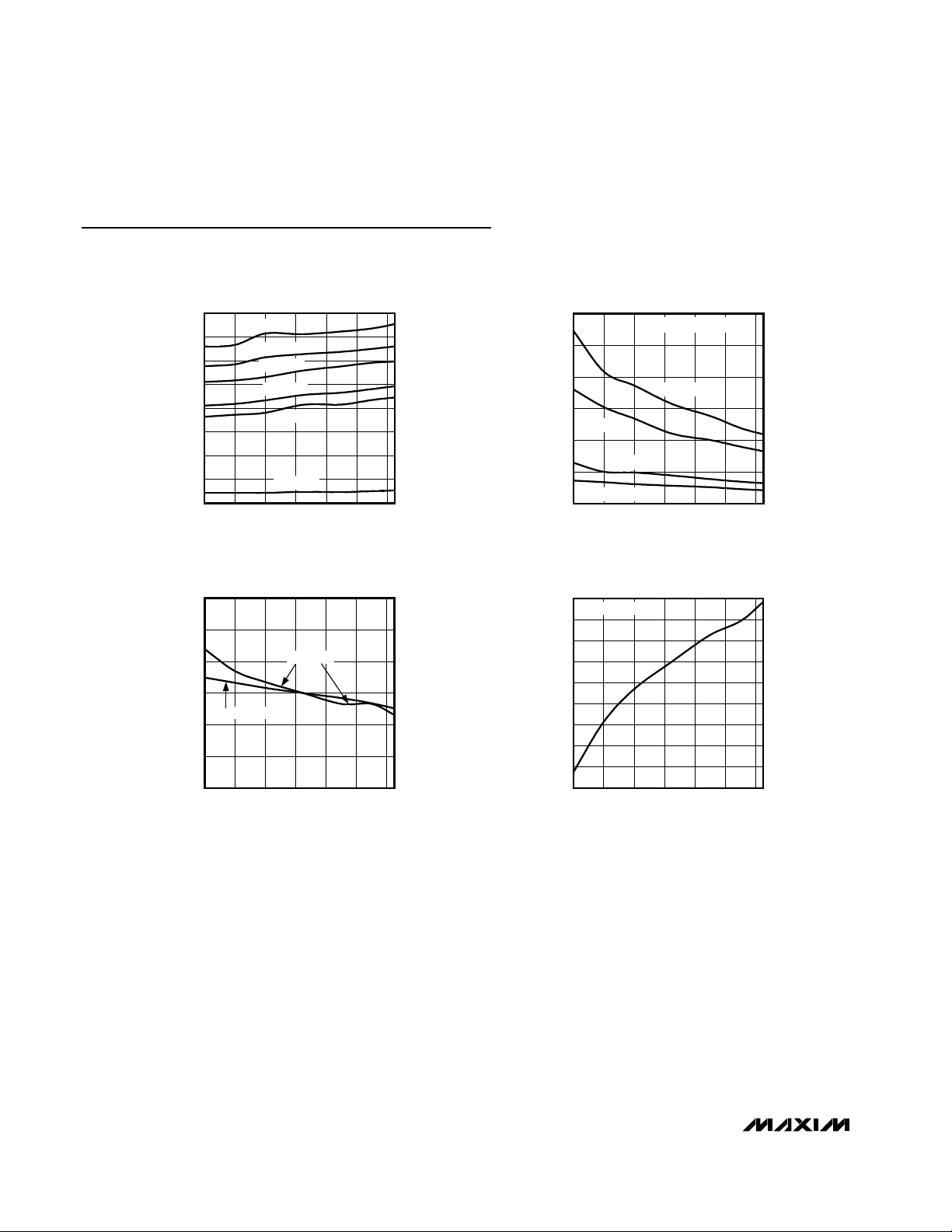
Typical Operating Characteristics
(VCC= full range and TA= -40°C to +85°C, unless otherwise noted. Typical values are at TA= +25°C).
SUPPLY CURRENT vs. TEMPERATURE
MAX6832-40 toc01
0
2
6
4
12
14
10
8
16
SUPPLY CURRENT (µA)
-40 0 20-20
40
60 80
TEMPERATURE (°C)
VCC = 3.6V
VCC = 3.0V
VCC = 2.5V
VCC = 1.8V
VCC = 1.5V
VCC = 0.55V
0
100
50
200
150
250
300
-40 20 40-20 0 60 80
POWER-DOWN RESET DELAY
vs. TEMPERATURE
MAX6832-40 toc02
TEMPERATURE (°C)
POWER-DOWN RESET DELAY (µs)
VOD = OVERDRIVE (mV)
VOD = 10mV
VOD = 20mV
VOD = 100mV
VOD = 200mV
0.994
0.996
0.995
0.999
0.998
0.997
1.002
1.001
1.000
1.003
-40 0-20 20 40 60 80
NORMALIZED RESET THRESHOLD
vs. TEMPERATURE
MAX6832-40 toc04
TEMPERATURE (°C)
NORMALIZED RESET THRESHOLD
VTH = 1.665V
0.94
0.98
0.96
1.02
1.00
1.04
1.06
-40 20 40-20 0 60 80
NORMALIZED POWER-UP RESET
TIMEOUT vs. TEMPERATURE
MAX6832-40 toc03
TEMPERATURE (°C)
NORMALIZED RESET TIMEOUT PERIOD
D1 OPTION
D2 OPTION
Page 5

MAX6832–MAX6840
Ultra-Low-Voltage SC70 Voltage Detectors
and µP Reset Circuits
_______________________________________________________________________________________ 5
Pin Description—MAX6832–MAX6837
Pin Description—MAX6838/MAX6839/MAX6840
PIN
MAX6833
SC70-3
1 1 1 1 GND Ground
— 2 — 2 RESET
2 — 2 — RESET
—— 33MR
3344VCCSupply Voltage and Monitored Supply
MAX6832/
MAX6834
SC70-3
MAX6836
SC70-4
MAX6835/
MAX6837
SC70-4
NAME FUNCTION
Reset Output, Open-Drain or Push-Pull, Active-Low. RESET
changes from HIGH to LOW when V
selected reset threshold or MR is pulled low. RESET remains
LOW for the reset timeout period after V
reset threshold and MR is released high.
Reset Output, Push-Pull, Active-High. RESET changes from
LOW to HIGH when the V
reset threshold or MR is pulled low. RESET remains HIGH for
the reset timeout period after V
threshold and MR is released high.
Active-Low Manual Reset Input. Internal 20kΩ pullup to V
Pull LOW to force a reset. Reset remains active as long as MR is
LOW and for the reset timeout period after MR goes HIGH.
Leave unconnected or connect to V
CC
drops below the
CC
exceeds the device
CC
input drops below the selected
exceeds the device reset
CC
CC
if unused.
CC
.
PIN
MAX6839
SC70-4
1 1 RESET-IN
22VCCSupply Voltage (1.1V to 3.3V)
3 3 GND
4 — RESET
— 4 RESET
MAX6838/
MAX6840
SC70-4
NAME FUNCTION
Adjustable Reset Threshold Input. High-impedance input for reset comparator. Connect
this pin to an external resistive-divider network to set the reset threshold voltage; the
typical threshold is 444mV. Reset is asserted when RESET-IN is below the threshold (V
is not monitored).
Ground
Reset Output, Push-Pull, Active-High. RESET changes from LOW to HIGH when the
RESET-IN input drops below the typical reset threshold (444mV). RESET remains HIGH for
the reset timeout period after RESET-IN exceeds the reset threshold.
Reset Output, Open-Drain or Push-Pull, Active-Low. RESET changes from HIGH to LOW
when RESET-IN drops below the typical reset threshold (444mV). RESET remains LOW for
the reset timeout period after RESET-IN exceeds the reset threshold.
CC
Page 6

MAX6832–MAX6840
Detailed Description
Reset Output
A microprocessor’s (µP’s) reset input starts the µP in a
known state. The MAX6832–MAX6840 assert a reset to
prevent code-execution errors during power-up, powerdown, or brownout conditions. They also assert a reset
signal whenever the VCCsupply voltage falls below a
preset threshold (MAX6832–MAX6837) or RESET-IN
falls below the adjustable threshold (MAX6838/
MAX6839/MAX6840), keeping reset asserted for a fixed
timeout delay (Table 2) after VCCor RESET-IN has risen
above the reset threshold. The MAX6832/MAX6835/
MAX6838 use a push-pull active-low output, the
MAX6833/MAX6836/MAX6839 have a push-pull activehigh output, and the MAX6834/MAX6837/MAX6840
have an open-drain active-low output stage. Connect a
pullup resistor on the MAX6834/MAX6837/MAX6840’s
RESET output to any supply between 0 and 6V.
Manual Reset Input
Many µP-based systems require manual reset capability, allowing the operator, a test technician, or external
logic circuitry to initiate a reset. Reset remains asserted
while MR is low, and for a fixed timeout delay after MR
returns high. This input has an internal 20kΩ pullup
resistor, so it can be left open if it is not used. MR can
be driven with CMOS logic level, or with open-drain/collector outputs. To create a manual reset function, connect a normally open momentary switch from MR to
ground; external debounce circuitry is not required. If
MR is driven from long cables or if the device is used in
a noisy environment, connecting a 0.1µF capacitor from
MR to ground provides additional noise immunity.
RESET-IN Information
The MAX6838/MAX6839/MAX6840 feature a RESET-IN
input for monitoring supply voltages down to 0.44V. An
external resistive-divider network can be used to set
voltage monitoring thresholds as shown in Figure 1. As
the monitored voltage falls, the voltage at RESET-IN
decreases and asserts a reset when it falls below the
RESET-IN threshold (V
RSTIN
). The low-leakage current
Ultra-Low-Voltage SC70 Voltage Detectors
and µP Reset Circuits
6 _______________________________________________________________________________________
Functional Diagrams
Figure 1. Setting the Adjustable Threshold Externally
MR (MAX6835/MAX6836/MAX6837 ONLY)
V
CC
MR
PULLUP
V
REF
= 444mV
MANUAL
RESET
DETECT
RESET
TIMEOUT
PERIOD
MAX6832–
MAX6837
RESET
OUTPUT
V
CC
RESET-IN
RESET/
RESET
= 444mV
V
REF
GND
V
MONITORED
R1
RESET-IN
R2
R1 = R2 [(V
MONITORED/VREF
WHERE V
MONITORED
= 444mV
V
REF
) -1]
IS THE DESIRED TRIP LEVEL,
RESET
TIMEOUT
PERIOD
MAX6838/
MAX6839/
MAX6840
RESET
OUTPUT
MAX6838/
MAX6839/
MAX6840
RESET
(RESET)
GND
V
( ) ARE FOR MAX6839
RESET/
RESET
GND
CC
Page 7

at RESET-IN allows for relatively large-value resistors to
be used, which reduce power consumption. For example, for a 0.6V monitored trip level, if R2 = 200kΩ, then
R1 = 70.3kΩ. Note that the minimum VCCof 1.1V is
required to guarantee the RESET-IN threshold accuracy (see Electrical Characteristics table).
Applications Information
Negative-Going VCCTransients
In addition to issuing a reset to the µP during power-up,
power-down, and brownout conditions, the MAX6832–
MAX6840 are relatively immune to short-duration negative-going VCCtransients (glitches).
Figure 2 shows typical transient duration vs. reset comparator overdrive, for which the MAX6832–MAX6840 do
not generate a reset pulse. The graph was generated
using a negative-going pulse applied to VCC, starting
0.1V above the actual reset threshold and ending
below it by the magnitude indicated (reset comparator
overdrive). The graph indicates the maximum pulse
width a negative-going VCCtransient can have without
causing a reset pulse. As the magnitude of the transient increases (goes farther below the reset threshold),
the maximum allowable pulse width decreases. A 0.1µF
bypass capacitor mounted as close as possible to the
VCCpin provides additional transient immunity.
Ensuring a Valid Reset Output
Down to V
CC
= 0
When VCCfalls below 0.55V, the MAX6832/MAX6835/
MAX6838 push-pull RESET output no longer sinks current—it becomes an open circuit. Therefore, highimpedance CMOS logic inputs connected to RESET
can drift to undetermined voltages. This presents no
problem in most applications since most µP and other
circuitry are inoperative with V
CC
lower than 0.55V.
However, in applications where RESET must be valid
down to 0, adding a pulldown resistor to RESET causes
any stray leakage currents to flow to ground, holding
RESET low (Figure 3). R3’s value is not critical; 100kΩ
is large enough not to load RESET and small enough to
pull RESET to ground.
A 100kΩ pullup resistor to VCCis also recommended
for the MAX6833/MAX6836/MAX6839 if RESET is
required to remain valid for VCC< 0.85V.
Interfacing to µPs with Bidirectional
Reset Pins
Since the RESET output on the MAX6834/MAX6837/
MAX6840 is open-drain, these devices interface easily
with µPs that have bidirectional reset pins. Connecting
the µP supervisor’s RESET output directly to the µP’s
RESET pin with a single pullup resistor allows either
device to assert a reset (Figure 4).
MAX6832–MAX6840
Ultra-Low-Voltage SC70 Voltage Detectors
and µP Reset Circuits
_______________________________________________________________________________________ 7
Figure 2. Maximum Transient Duration Without Causing a
Reset Pulse vs. Reset Comparator Overdrive
Figure 3.
RESET
Valid to VCC= Ground Circuit
Figure 4. Interfacing to µPs with Bidirectional Reset I/O
MAXIMUM TRANSIENT DURATION
vs. OVERDRIVE
900
800
700
600
500
400
300
200
MAXIMUM TRANSIENT DURATION (µs)
100
0
1 10 100
OVERDRIVE VTH - VCC (mV)
RESET OCCURS
ABOVE THIS
LINE
V
CC
MAX6832
MAX6835
MAX6838
GND
RESET
R3
100kΩ
V
CC
V
CC
MAX6834
MAX6837
MAX6840
GND
RESET
RESET
INPUT
V
CC
BIDIRECTIONAL
µP
GND
Page 8

MAX6832–MAX6840
Using The MAX6834/MAX6837/MAX6840
Open-Drain
RESET
Output
with Multiple Supplies
Generally, the pullup connected to the MAX6834/
MAX6837/MAX6840 will connect to the supply voltage
that is being monitored at the IC’s VCCpin. However,
some systems may use the open-drain output to levelshift from the monitored supply to reset circuitry powered by some other supply (Figure 5). Note that as the
MAX6834/MAX6837/MAX6840’s VCCdecreases, so
does the IC’s ability to sink current at RESET. Also, with
any pullup, RESET will be pulled high as V
CC
declines
toward 0. The voltage where this occurs depends on
the pullup resistor value and the voltage to which it is
connected.
Chip Information
TRANSISTOR COUNT: 681
PROCESS: BiCMOS
Ultra-Low-Voltage SC70 Voltage Detectors
and µP Reset Circuits
8 _______________________________________________________________________________________
Figure 5. Using The MAX6834/MAX6837/MAX6840 Open-Drain
RESET
Output with Multiple Supplies
Table 2. Active Timeout Period Guide
Table 3. Standard Versions
Table 1. Threshold Suffix Guide
Selector Guide
+1.2V
+5.0V
RESET
INPUT
V
CC
5V SYSTEM
GND
V
CC
R
PULLUP
MAX6834
MAX6837
MAX6840
RESET
GND
SUFFIX RESET THRESHOLD (V)
W 1.665
V 1.575
I 1.388
H 1.313
G 1.110
F 1.050
SUFFIX
D0 0.07
D1 1.5
D2 30
D3 210
D4 1680
DEVICE TOP MARK
MAX6832VXRD0 AIQ
MAX6832VXRD3 AIR
MAX6832HXRD0 AIS
MAX6832HXRD3 AIT
MAX6832FXRD0 AIU
MAX6832FXRD3 AIV
MAX6833VXRD0 AHJ
MAX6833VXRD3 AIW
MAX6833HXRD0 AIX
MAX6833HXRD3 AIY
MAX6833FXRD0 AIZ
MAX6833FXRD3 AJA
MAX6834VXRD0 AJB
MAX6834VXRD3 AJC
MAX6834HXRD0 AJD
MAX6834HXRD3 AJE
MAX6834FXRD0 AJF
MAX6834FXRD3 AJG
MAX6835VXSD0 AEX
TYPICAL RESET ACTIVE
TIMEOUT PERIOD (ms)
Page 9

MAX6832–MAX6840
Ultra-Low-Voltage SC70 Voltage Detectors
and µP Reset Circuits
_______________________________________________________________________________________ 9
Typical Operating Circuit
Pin Configurations
Table 3. Standard Versions (continued)
Selector Guide (continued)
TOP VIEW
GND
RESET (RESET)
V
IN
3.3V
1
MAX6832
MAX6833
MAX6834
2
SC70-3
( ) ARE FOR MAX6833
V
CC
3
GND
RESET (RESET)
DC/DC
CONVERTER
1.2V
V
MAX6834G/F
GND
CC
RESET
CORE
SUPPLY
RESET
µP
GND
1
MAX6835
MAX6836
MAX6837
2
SC70-4
( ) ARE FOR MAX6836
I/O
SUPPLY
V
4
CC
MR
3
RESET-IN
1
MAX6838
MAX6839
MAX6840
2
V
CC
SC70-4
( ) ARE FOR MAX6839
4
RESET (RESET)
3 GND
DEVICE TOP MARK
MAX6835VXSD3 AFF
MAX6835HXSD0 AFG
MAX6835HXSD3 AFH
MAX6835FXSD0 AFI
MAX6835FXSD3 AFJ
MAX6836VXSD0 AFK
MAX6836VXSD3 AFL
MAX6836HXSD0 AFM
MAX6836HXSD3 AFN
MAX6836FXSD0 AFO
MAX6836FXSD3 AFP
MAX6837VXSD0 AFQ
MAX6837VXSD3 AFR
MAX6837HXSD0 AFS
MAX6837HXSD3 AFT
MAX6837FXSD0 AFU
MAX6837FXSD3 AFC
MAX6838XSD0 AFW
MAX6838XSD3 AFV
MAX6839XSD0 AFX
MAX6839XSD3 AEZ
MAX6840XSD0 AFY
MAX6840XSD3 AFZ
Page 10

MAX6832–MAX6840
Ultra-Low-Voltage SC70 Voltage Detectors
and µP Reset Circuits
10 ______________________________________________________________________________________
Package Information
,
3L.EPS
SC70
Page 11

MAX6832–MAX6840
Ultra-Low-Voltage SC70 Voltage Detectors
and µP Reset Circuits
Maxim cannot assume responsibility for use of any circuitry other than circuitry entirely embodied in a Maxim product. No circuit patent licenses are
implied. Maxim reserves the right to change the circuitry and specifications without notice at any time.
Maxim Integrated Products, 120 San Gabriel Drive, Sunnyvale, CA 94086 408-737-7600 ____________________ 11
© 2001 Maxim Integrated Products Printed USA is a registered trademark of Maxim Integrated Products.
Package Information (continued)
SC70, 4L.EPS
 Loading...