

General Description
The MAX6715–MAX6729 are ultra-low-voltage microprocessor (µP) supervisory circuits designed to monitor two or three
system power-supply voltages. These devices assert a system reset if any monitored supply falls below its factorytrimmed or adjustable threshold and maintain reset for a
minimum timeout period after all supplies rise above their
thresholds. The integrated dual/triple supervisory circuits significantly improve system reliability and reduce size compared to separate ICs or discrete components.
These devices monitor primary supply voltages (VCC1) from
1.8V to 5.0V and secondary supply voltages (VCC2) from
0.9V to 3.3V with factory-trimmed reset threshold voltage
options (see Reset Voltage Threshold Suffix Guide). An
externally adjustable RSTIN input option allows customers to
monitor a third supply voltage down to 0.62V. These devices
are guaranteed to be in the correct reset output logic state
when either VCC1 or VCC2 remains greater than 0.8V.
A variety of push-pull or open-drain reset outputs along with
watchdog input, manual reset input, and power-fail input/output features are available (see Selector Guide). Select reset
timeout periods from 1.1ms to 1120ms (min) (see Reset
Timeout Period Suffix Guide). The MAX6715–MAX6729 are
available in small 5, 6, and 8-pin SOT23 packages and operate over the -40°C to +85°C temperature range.
Applications
Multivoltage Systems
Telecom/Networking Equipment
Computers/Servers
Portable/Battery-Operated Equipment
Industrial Equipment
Printer/Fax
Set-Top Boxes
Features
♦ VCC1 (primary supply) Reset Threshold Voltages
from 1.58V to 4.63V
♦ VCC2 (secondary supply) Reset Threshold
Voltages from 0.79V to 3.08V
♦ Externally Adjustable RSTIN Threshold for
Auxiliary/Triple-Voltage Monitoring
(0.62V internal reference)
♦ Watchdog Timer Option
35s (min) Long Startup Period
1.12s (min) Normal Timeout Period
♦ Manual Reset Input Option
♦ Power-Fail Input/Power-Fail Output Option
(Push-Pull and Open-Drain Active-Low)
♦ Guaranteed Reset Valid Down to VCC1 or
VCC2 = 0.8V
♦ Reset Output Logic Options
♦ Immune to Short VCCTransients
♦ Low Supply Current 14µA (typ) at 3.6V
♦ Small 5, 6, and 8-Pin SOT23 Packages
MAX6715–MAX6729
Dual/Triple Ultra-Low-Voltage SOT23 µP
Supervisory Circuits
________________________________________________________________ Maxim Integrated Products 1
Ordering Information
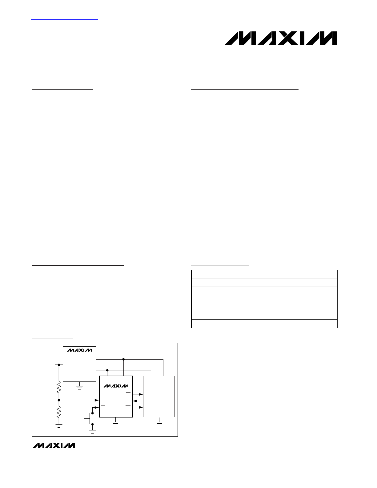
IN
OUT2
OUT1
DC/DC
CONVERTER
UNREGULATED
DC
R1
R2
VCC1VCC2
RSTIN/PFI
MR
RST
WDI
PFO
MAX67_ _
PUSHBUTTON
SWITCH
I/O
SUPPLY
CORE
SUPPLY
RESET
I/O
NMI
µP
1.8V 0.9V
Typical Operating Circuit
19-2325; Rev 3; 6/03
For pricing, delivery, and ordering information, please contact Maxim/Dallas Direct! at
1-888-629-4642, or visit Maxim’s website at www.maxim-ic.com.
Pin Configurations appear at end of data sheet.
Selector Guide appears at end of data sheet.
Note: The first “_ _” are placeholders for the threshold voltage
levels of the devices. Desired threshold levels are set by the part
number suffix found in the Reset Voltage Threshold Suffix Guide.
The “_” after the D is a placeholder for the reset timeout delay
time. Desired delay time is set using the timeout period suffix
found in the Reset Timeout Period Suffix Guide. For example the
MAX6716UTLTD3-T is a dual-voltage supervisor V
TH
1 = 4.625V,
V
TH
2 = 3.075V, and 210ms (typ) timeout period.
Ordering Information continued at end of data sheet.
查询MAX6715供应商
PART TEMP RANGE PIN-PACKAGE
MAX6715UT_ _D_ -T -40°C to +85°C 6 SOT23-6
MAX6716UT_ _D_ -T -40°C to +85°C 6 SOT23-6
MAX6717UK_ _D_ -T -40°C to +85°C 5 SOT23-5
MAX6718UK_ _D_ -T -40°C to +85°C 5 SOT23-5
MAX6719UT_ _D_ -T -40°C to +85°C 6 SOT23-6
MAX6720UT_ _D_ -T -40°C to +85°C 6 SOT23-6
MAX6715–MAX6729
Dual/Triple Ultra-Low-Voltage SOT23 µP
Supervisory Circuits
2 _______________________________________________________________________________________
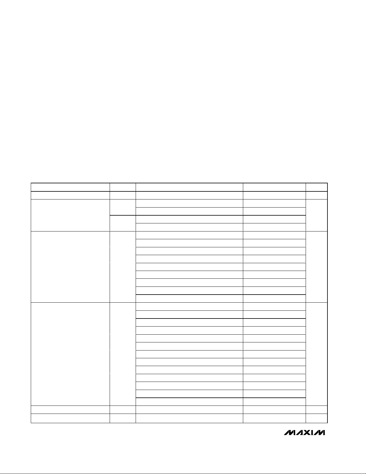
ABSOLUTE MAXIMUM RATINGS
ELECTRICAL CHARACTERISTICS
(VCC1 = VCC2 = 0.8V to 5.5V, GND = 0, TA= -40°C to +85°C, unless otherwise noted. Typical values are at TA= +25°C.) (Note 1)
Stresses beyond those listed under “Absolute Maximum Ratings” may cause permanent damage to the device. These are stress ratings only, and functional
operation of the device at these or any other conditions beyond those indicated in the operational sections of the specifications is not implied. Exposure to
absolute maximum rating conditions for extended periods may affect device reliability.
Terminal Voltage (with respect to GND)
VCC1, VCC2 ..........................................................-0.3V to +6V
Open-Drain RST, RST1, RST2, PFO, RST ................-0.3V to +6V
Push-Pull RST, RST1, PFO, RST...............-0.3V to (V
CC
1 + 0.3V)
Push-Pull RST2 .........................................-0.3V to (V
CC
2 + 0.3V)
RSTIN, PFI, MR, WDI ................................................-0.3V to +6V
Input Current/Output Current (all pins) ...............................20mA
Continuous Power Dissipation (T
A
= +70°C)
5-Pin SOT23-5 (derate 7.1mW/°C above +70°C) ........571mW
6-Pin SOT23-6 (derate 8.7mW/°C above +70°C) ........696mW
8-Pin SOT23-8 (derate 8.9mW/°C above +70°C) ........714mW
Operating Temperature Range ...........................-40°C to +85°C
Storage Temperature Range .............................-65°C to +150°C
Junction Temperature......................................................+150°C
Lead Temperature (soldering, 10s) .................................+300°C
Supply Voltage V
Supply Current
VCC1 Reset Threshold V
VCC2 Reset Threshold V
Reset Threshold Tempco 20 ppm/°C
Reset Threshold Hysteresis V
PARAMETER SYMBOL CONDITIONS MIN TYP MAX UNITS
CC
I
CC1
I
CC2
TH1
TH2
HYST
VCC1 < 5.5V, all I/O pins open 15 39
VCC1 < 3.6V, all I/O pins open 10 28
VCC2 < 3.6V, all I/O pins open 4 11
VCC2 < 2.75V, all I/O pins open 3 9
L (falling) 4.500 4.625 4.750
M (falling) 4.250 4.375 4.500
T (falling) 3.000 3.075 3.150
S (falling) 2.850 2.925 3.000
R (falling) 2.550 2.625 2.700
Z (falling) 2.250 2.313 2.375
Y (falling) 2.125 2.188 2.250
W (falling) 1.620 1.665 1.710
V (falling) 1.530 1.575 1.620
T (falling) 3.000 3.075 3.150
S (falling) 2.850 2.925 3.000
R (falling) 2.550 2.625 2.700
Z (falling) 2.250 2.313 2.375
Y (falling) 2.125 2.188 2.250
W (falling) 1.620 1.665 1.710
V (falling) 1.530 1.575 1.620
I (falling) 1.350 1.388 1.425
H (falling) 1.275 1.313 1.350
G (falling) 1.080 1.110 1.140
F (falling) 1.020 1.050 1.080
E (falling) 0.810 0.833 0.855
D (falling) 0.765 0.788 0.810
Referenced to VTH typical 0.5 %
0.8 5.5 V
µA
V
V
MAX6715–MAX6729
Dual/Triple Ultra-Low-Voltage SOT23 µP
Supervisory Circuits
_______________________________________________________________________________________ 3
ELECTRICAL CHARACTERISTICS (continued)
(VCC1 = VCC2 = 0.8V to 5.5V, GND = 0, TA= -40°C to +85°C, unless otherwise noted. Typical values are at TA= +25°C.) (Note 1)
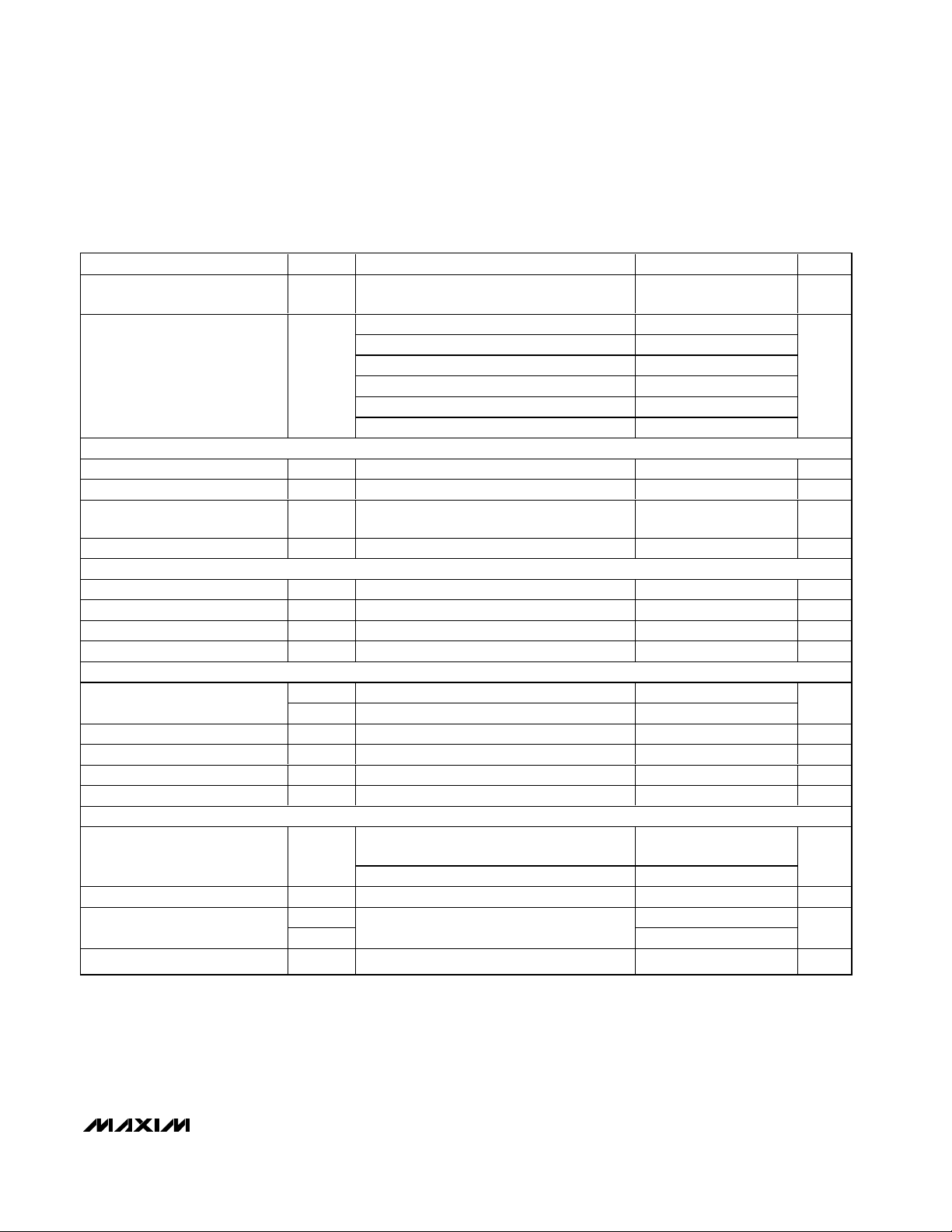
VCC to Reset Output Delay t
Reset Timeout Period t
ADJUSTABLE RESET COMPARATOR INPUT (MAX6719/MAX6720/MAX6723–MAX6727)
RSTIN Input Threshold V
RSTIN Input Current I
RSTIN Hysteresis 3mV
RSTIN to Reset Output Delay t
POWER-FAIL INPUT (MAX6728/MAX6729)
PFI Input Threshold V
PFI Input Current I
PFI Hysteresis V
PFI to PFO Delay t
MANUAL RESET INPUT (MAX6715–MAX6722/MAX6725–MAX6729)
MR Input Voltage
MR Minimum Pulse Width 1µs
MR Glitch Rejection 100 ns
MR to Reset Delay t
MR Pullup Resistance 25 50 80 kΩ
WATCHDOG INPUT (MAX6721–MAX6729)
Watchdog Timeout Period t
WDI Pulse Width t
WDI Input Voltage
WDI Input Current I
PARAMETER SYMBOL CONDITIONS MIN TYP MAX UNITS
V
1 = ( V
RD
RP
RSTIN
RSTIN
RSTINDVRSTIN
PFI
PFI
PFH
DPF
V
IL
V
IH
MR
WD
WDI
V
IL
V
IH
WDI
C C
2 = ( V
V
C C
D1 1.1 1.65 2.2
D2 8.8 13.2 17.6
D3 140 210 280
D5 280 420 560
D6 560 840 1120
D4 1120 1680 2240
(V
PFI
First watchdog period after reset timeout
period
Normal mode 1.12 1.68 2.24
(Note 2) 50 ns
WDI = 0 or VCC1-1+1µA
1 + 100m V ) to ( V
TH
2 + 75m V ) to ( V
TH
to (V
RSTIN
+ 30mV) to (V
- 30mV) 22 µs
PFI
1 - 100m V ) or
TH
2 - 75m V )
TH
611 626.5 642 mV
-25 +25 nA
611 626.5 642 mV
-25 +25 nA
- 30mV) 2 µs
0.7 ✕ VCC1
35 54 72
0.7 ✕ VCC1
20 µs
ms
3mV
0.3 ✕ VCC1
200 ns
0.3 ✕ VCC1
V
s
V
MAX6715–MAX6729
Dual/Triple Ultra-Low-Voltage SOT23 µP
Supervisory Circuits
4 _______________________________________________________________________________________
Note 1: Devices tested at +25°C. Overtemperature limits are guaranteed by design and not production tested.
Note 2: Parameter guaranteed by design.
ELECTRICAL CHARACTERISTICS (continued)
(VCC1 = VCC2 = 0.8V to 5.5V, GND = 0, TA= -40°C to +85°C, unless otherwise noted. Typical values are at TA= +25°C.) (Note 1)
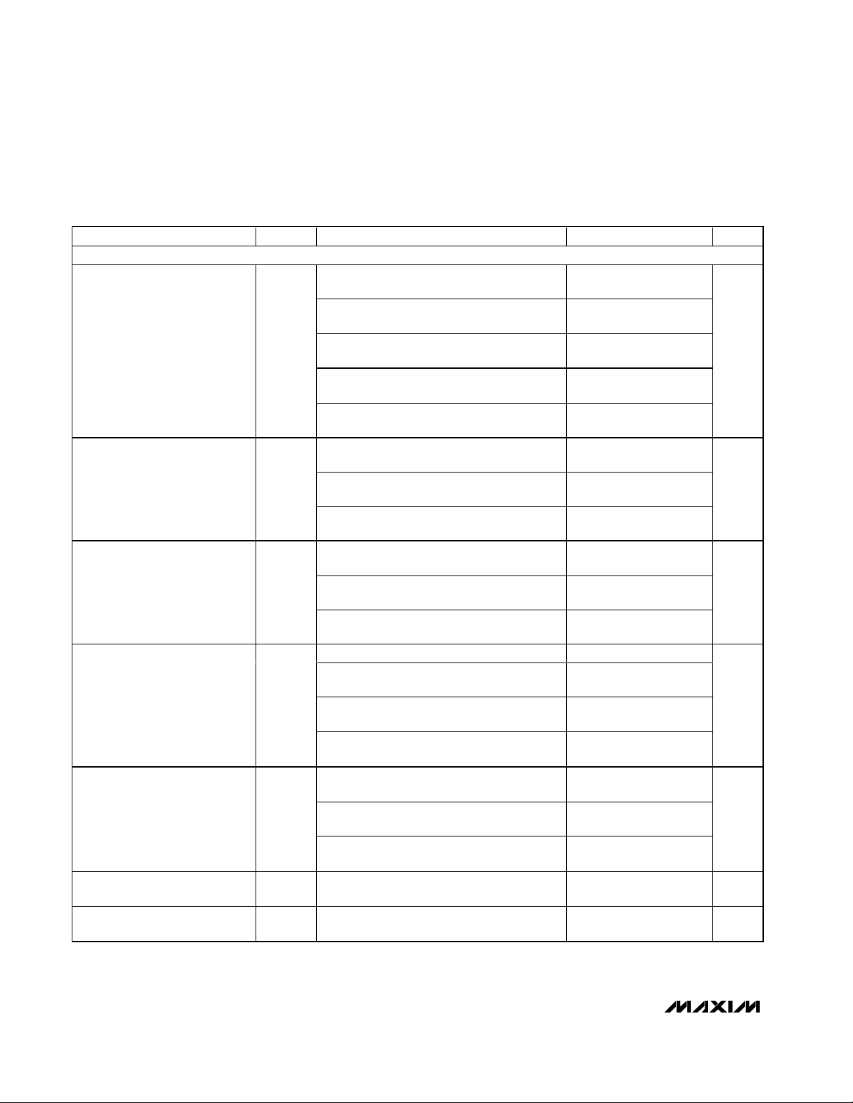
RESET/POWER-FAIL OUTPUTS
RST/RST1/RST2/PFO
Output LOW
(Push-Pull or Open-Drain)
RST/RST1/PFO
Output HIGH
(Push-Pull Only)
RST2
Output HIGH
(Push-Pull Only)
RST
Output HIGH
(Push-Pull Only)
RST
Output LOW
(Push-Pull or Open Drain)
RST/RST1/RST2/PFO Output
Open-Drain Leakage Current
RST Output Open-Drain
Leakage Current
PARAMETER SYMBOL CONDITIONS MIN TYP MAX UNITS
VCC1 or VCC2 ≥ 0.8V, I
output asserted
VCC1 or VCC2 ≥ 1.0V, I
output asserted
V
OL
VCC1 or VCC2 ≥ 1.2V, I
output asserted
VCC1 or VCC2 ≥ 2.7V, I
output asserted
VCC1 or VCC2 ≥ 4.5V, I
output asserted
VCC1 ≥ 1.8V, I
SOURCE
asserted
V
OH
VCC1 ≥ 2.7V, I
asserted
VCC1 ≥ 4.5V, I
SOURCE
SOURCE
asserted
VCC2 ≥ 1.8V, I
SOURCE
asserted
V
OH
VCC2 ≥ 2.7V, I
asserted
VCC2 ≥ 4.5V, I
SOURCE
SOURCE
asserted
VCC1 ≥ 1.0V, I
VCC1 ≥ 1.8V, I
SOURCE
SOURCE
reset asserted
V
OH
VCC1 ≥ 2.7V, I
SOURCE
reset asserted
VCC1 ≥ 4.5V, I
SOURCE
reset asserted
VCC1 or VCC2 ≥ 1.8V, I
reset not asserted
V
OL
VCC1 or VCC2 ≥ 2.7V, I
reset not asserted
VCC1 or VCC2 ≥ 4.5V, I
reset not asserted
= 1µA,
SINK
= 50µA,
SINK
= 100µA,
SINK
= 1.2mA,
SINK
= 3.2mA,
SINK
= 200µA, output not
= 500µA, output not
= 800µA, output not
= 200µA, output not
= 500µA, output not
= 800µA, output not
0.8
0.8
0.8
0.8
0.8
0.8
✕ V
✕ V
✕ V
✕ V
✕ V
✕ V
CC
CC
CC
CC
CC
CC
= 1µA, reset asserted 0.8 ✕ VCC1
= 150µA,
= 500µA,
= 800µA,
= 500µA,
SINK
= 1.2mA,
SINK
= 3.2mA,
SINK
0.8
0.8
0.8
✕ V
✕ V
✕ V
CC
CC
CC
0.3
0.3
0.3
0.3
0.4
1
1
1
2
2
2
1
1
1
0.3
0.3
0.4
Output not asserted 0.5 µA
Output asserted 0.5 µA
V
V
V
V
V
MAX6715–MAX6729
Dual/Triple Ultra-Low-Voltage SOT23 µP
Supervisory Circuits
_______________________________________________________________________________________ 5
Typical Operating Characteristics
(VCC1 = 5V, VCC2 = 3.3V, TA= +25°C, unless otherwise noted.)
SUPPLY CURRENT vs. TEMPERATURE
1 = 5V, VCC2 = 3.3V
V
18
16
14
12
10
8
6
SUPPLY CURRENT (µA)
4
2
0
-40 10-15 356085
CC
TOTAL
ICC1
ICC2
TEMPERATURE (°C)
SUPPLY CURRENT vs. TEMPERATURE
1 = 1.8V, VCC2 = 1.2V
V
18
16
14
12
10
8
6
SUPPLY CURRENT (µA)
4
2
0
CC
TOTAL
ICC1
ICC2
-40 10-15 356085
TEMPERATURE (°C)
NORMALIZED VCC RESET THRESHOLD
vs. TEMPERATURE
1.004
1.003
1.002
1.001
1.000
0.999
RESET THRESHOLD
0.998
0.997
0.996
-40 -15 10 35 60 85
TEMPERATURE (°C)
MAX6715-29 toc01
MAX6715-29 toc04
MAX6715-29 toc07
SUPPLY CURRENT vs. TEMPERATURE
V
18
16
14
12
10
8
6
SUPPLY CURRENT (µA)
4
2
0
CC
-40 10-15 356085
NORMALIZED RESET/WATCHDOG
TIMEOUT PERIOD vs. TEMPERATURE
1.007
1.006
1.005
1.004
1.003
1.002
1.001
RESET/WATCHDOG PERIOD
1.000
0.999
0.998
-40 10-15 356085
RESET INPUT AND POWER-FAIL INPUT
THRESHOLD vs. TEMPERATURE
631
630
629
628
THRESHOLD (mV)
627
626
625
-40 85
1 = 3.3V, VCC2 = 2.5V
TOTAL
ICC1
ICC2
TEMPERATURE (°C)
TEMPERATURE (°C)
10-15 35 60
TEMPERATURE (°C)
MAX6715-29 toc02
10,000
MAX6715-29 toc05
TRANSIENT DURATION (µs)
CC
MAXIMUM V
MAX6715-29 toc08
SUPPLY CURRENT vs. TEMPERATURE
1 = 2.5V, VCC2 = 1.8V
V
18
16
14
12
10
8
6
SUPPLY CURRENT (µA)
4
2
0
CC
TOTAL
ICC1
ICC2
-40 10-15 356085
TEMPERATURE (°C)
MAXIMUM VCC TRANSIENT DURATION
vs. RESET THRESHOLD OVERDRIVE
RESET OCCURS ABOVE
THIS LINE
1000
100
10
110010 1000
RESET THRESHOLD OVERDRIVE (mV)
VCC TO RESET DELAY
vs. TEMPERATURE
54
53
52
51
50
49
48
TO RESET DELAY (µs)
47
CC
V
46
45
44
-40 10-15 35 60 85
TEMPERATURE (°C)
100mV OVERDRIVE
MAX6715-29 toc03
MAX6715-29 toc06
MAX6715-29 toc09
MAX6715–MAX6729
Dual/Triple Ultra-Low-Voltage SOT23 µP
Supervisory Circuits
6 _______________________________________________________________________________________
Pin Description
22.8
23.0
23.2
23.4
23.6
23.8
24.0
24.2
24.4
-40 -15 10 35 60 85
RESET INPUT TO RESET OUTPUT DELAY
vs. TEMPERATURE
MAX6715-29 toc10
TEMPERATURE (°C)
RSTIN TO RESET DELAY (µs)
30mV OVERDRIVE
2.0
2.1
2.2
2.4
2.3
-40 10-15 35 60 85
POWER-FAIL INPUT TO POWER-FAIL
OUTPUT DELAY vs. TEMPERATURE
MAX6715-29 toc11
TEMPERATURE (°C)
RSTIN TO RESET DELAY (µs)
30mV OVERDRIVE
0
0
V
RST
2V/div
MAX6715-29 toc12
50ns/div
MR TO RESET OUTPUT DELAY
V
MR
2V/div
Typical Operating Characteristics (continued)
(VCC1 = 5V, VCC2 = 3.3V, TA= +25°C, unless otherwise noted.)
MAX6715/
MAX6716
MAX6717/
MAX6718
1111111, 41
MAX6719/
MAX6720
MAX6721/
MAX6722
PIN
MAX6723/
MAX6724
MAX6725/
MAX6726
MAX6727
MAX6728/
MAX6729
NAME FUNCTION
Active-Low Reset Output,
Open-Drain or Push-Pull.
RST/RST1 changes from
high to low when V
V
2 drops below the
CC
selected reset thresholds,
RSTIN is below threshold,
MR is pulled low, or the
watchdog triggers a
reset. RST/RST1 remains
RST/
low for the reset timeout
RST1
period after V
V
2/RSTIN exceed the
CC
device reset thresholds,
MR goes low to high, or
the watchdog triggers a
reset. Open-drain outputs
require an external pullup
resistor. Push-pull
outputs are referenced to
V
1.
CC
CC
1/
CC
1 or

MAX6715–MAX6729
Dual/Triple Ultra-Low-Voltage SOT23 µP
Supervisory Circuits
_______________________________________________________________________________________ 7
Pin Description (continued)
PIN
MAX6715/
MAX6716
MAX6717/
MAX6718
5 ———————RST2
22222222GNDGround
3333— 555MR
44444666V
65666888V
MAX6719/
MAX6720
MAX6721/
MAX6722
MAX6723/
MAX6724
MAX6725/
MAX6726
MAX6727
MAX6728/
MAX6729
NAME FUNCTION
2
CC
1
CC
Active-Low Reset Output,
Open-Drain or Push-Pull.
RST2 changes from high
to low when V
V
2 drops below the
CC
selected reset thresholds
or MR is pulled low. RST2
remains low for the reset
timeout period after
1/VCC2 exceed the
V
CC
device reset thresholds
or MR goes low to high.
Open-drain outputs
require an external pullup
resistor. Push-pull
outputs are referenced to
2.
V
CC
Active-Low Manual Reset
Input. Internal 50kΩ
pullup to V
to force a reset. Reset
remains active as long as
MR is low and for the
reset timeout period after
MR goes high. Leave
unconnected or connect
to V
1 if unused.
CC
Secondary Supply
Voltage Input. Powers the
device when it is above
1 and input for
V
CC
secondary reset
threshold monitor.
Primary Supply Voltage
Input. Powers the device
when it is above VCC2
and input for primary
reset threshold monitor.
CC
1. Pull low
CC
1 or

MAX6715–MAX6729
Dual/Triple Ultra-Low-Voltage SOT23 µP
Supervisory Circuits
8 _______________________________________________________________________________________
Pin Description (continued)
PIN
MAX6715/
MAX6716
MAX6717/
MAX6718
——— 53333WDI
MAX6719/
MAX6720
MAX6721/
MAX6722
—— 5 — 577— RSTIN
——————— 7 PFI
MAX6723/
MAX6724
MAX6725/
MAX6726
MAX6727
MAX6728/
MAX6729
NAME FUNCTION
Watchdog Input. If WDI
remains high or low for
longer than the watchdog
timeout period, the
internal watchdog timer
runs out and the reset
output asserts for the
reset timeout period. The
internal watchdog timer
clears whenever a reset
is asserted or WDI sees a
rising or falling edge. The
watchdog has a long
timeout period (35s min)
after each reset event
and a short timeout
period (1.12s min) after
the first valid WDI
transition. Leave WDI
floating to disable the
watchdog timer function.
Undervoltage Reset
Comparator Input. Highimpedance input for
adjustable reset monitor.
The reset output is
asserted when RSTIN falls
below the 0.626V internal
reference voltage. Set the
monitored voltage reset
threshold with an external
resistor-divider network.
Connect RSTIN to V
V
2 if not used.
CC
Power-Fail Voltage
Monitor Input. Highimpedance input for
internal power-fail monitor
comparator. Connect PFI
to an external resistordivider network to set the
power-fail threshold
voltage (0.626V typical
internal reference
voltage). Connect to
GND, V
not used.
1, or VCC2 if
CC
CC
1 or

Detailed Description
Supply Voltages
The MAX6715–MAX6729 microprocessor (µP) supervisory circuits maintain system integrity by alerting the µP
to fault conditions. These ICs are optimized for systems
that monitor two or three supply voltages. The outputreset state is guaranteed to remain valid while either
VCC1 or VCC2 is above 0.8V.
Threshold Levels
Input voltage threshold level combinations are indicated by a two-letter code in the Reset Voltage Threshold
Suffix Guide (Table 1). Contact factory for availability of
other voltage threshold combinations.
Reset Outputs
The MAX6715–MAX6729 provides an active-low reset
output (RST) and the MAX6725/MAX6726 provides
both an active-high (RST) and an active-low reset output (RST). RST, RST, RST1, and RST2 are asserted
when the voltage at either VCC1 or VCC2 falls below the
voltage threshold level, RSTIN drops below threshold,
or MR is pulled low. Once reset is asserted it stays low
for the reset timeout period (see Table 2). If VCC1,
V
CC
2, or RSTIN goes below the reset threshold before
the reset timeout period is completed, the internal timer
MAX6715–MAX6729
Dual/Triple Ultra-Low-Voltage SOT23 µP
Supervisory Circuits
_______________________________________________________________________________________ 9
Pin Description (continued)
PIN
MAX6715/
MAX6716
MAX6717/
MAX6718
——————— 4 PFO
————— 4 ——RST
MAX6719/
MAX6720
MAX6721/
MAX6722
MAX6723/
MAX6724
MAX6725/
MAX6726
MAX6727
MAX6728/
MAX6729
NAME FUNCTION
Active-Low Power-Fail
Monitor Output, OpenDrain or Push-Pull. PFO is
asserted low when PFI is
less than 0.626V. PFO
deasserts without a reset
timeout period. Opendrain outputs require an
external pullup resistor.
Push-pull outputs are
referenced to V
Active-High Reset
Output, Open-Drain or
Push-Pull. RST changes
from low to high when
V
1 or VCC2 drops
CC
below selected reset
thresholds, RSTIN is
below threshold, MR is
pulled low, or the
watchdog triggers a
reset. RST remains HIGH
for the reset timeout
period after V
2/RSTIN exceed the
V
CC
device reset thresholds,
MR goes low to high, or
the watchdog triggers a
reset. Open-drain outputs
require an external pullup
resistor. Push-pull
outputs are referenced to
V
1.
CC
CC
CC
1/
1.

MAX6715–MAX6729
restarts. The MAX6715/MAX6717/MAX6719/MAX6721/
MAX6723/MAX6725/MAX6727/MAX6728 contain opendrain reset outputs, while the MAX6716/MAX6718/
MAX6720/MAX6722/MAX6724/MAX6726/MAX6729
contain push-pull reset outputs. The MAX6727 provides
two separate open-drain RST outputs driven by the
same internal logic.
Manual Reset Input
Many microprocessor-based products require manual
reset capability, allowing the operator, a test technician, or external logic circuitry to initiate a reset. A logic
low on MR asserts the reset output. Reset remains
asserted while MR is low and for the reset timeout period (tRP) after MR returns high. This input has an internal
50kΩ pullup resistor to VCC1 and can be left unconnected if not used. MR can be driven with TTL or
CMOS logic levels, or with open-drain/collector outputs.
Connect a normally open momentary switch from MR to
GND to create a manual reset function; external
debounce circuitry is not required. If MR is driven from
long cables or if the device is used in a noisy environment, connect a 0.1µF capacitor from MR to GND to
provide additional noise immunity.
Adjustable Input Voltage
The MAX6719/MAX6720 and MAX6723–MAX6727 provide
an additional input to monitor a third system voltage. The
threshold voltage at RSTIN is typically 626mV. Connect a
resistor-divider network to the circuit as shown in Figure 1
to establish an externally controlled threshold voltage,
V
EXT_TH
.
V
EXT_TH
= 626mV((R1 + R2)/R2)
Low leakage current at RSTIN allows the use of largevalued resistors resulting in reduced power consumption of the system.
Watchdog Input
The watchdog monitors µP activity through the watchdog input (WDI). To use the watchdog function, connect WDI to a bus line or µP I/O line. When WDI
remains high or low for longer than the watchdog timeout period, the reset output asserts. Leave WDI floating
to disable the watchdog function.
The MAX6721–MAX6729 include a dual-mode watchdog timer to monitor µP activity. The flexible timeout
architecture provides a long period initial watchdog
mode, allowing complicated systems to complete
lengthy boots, and a short period normal watchdog
mode, allowing the supervisor to provide quick alerts
when processor activity fails. After each reset event
(V
CC
power-up/brownout, manual reset, or watchdog
reset), there is a long initial watchdog period of 35s
minimum. The long watchdog period mode provides an
extended time for the system to power-up and fully initialize all µP and system components before assuming
responsibility for routine watchdog updates.
The normal watchdog timeout period (1.12s min)
begins after the first transition on WDI before the conclusion of the long initial watchdog period (Figure 2).
During the normal operating mode, the supervisor will
issue a reset pulse for the reset timeout period if the µP
does not update the WDI with a valid transition (high-tolow or low-to-high) within the standard timeout period
(1.12s min).
Power-Fail Comparator
PFI is the noninverting input to a comparator. If PFI is
less than V
PFI
(626.5mV), PFO goes low. Common uses
for the power-fail comparator include monitoring preregulated input of the power supply (such as a battery) or
Dual/Triple Ultra-Low-Voltage SOT23 µP
Supervisory Circuits
10 ______________________________________________________________________________________
Figure 1. Monitoring a Third Voltage
Figure 2. Normal Watchdog Startup Sequence
V
EXT_TH
R1
RSTIN
R2
V
TH
V
CC
WDI
RESET
t
WDI-NORMAL
1.12s MAX
t
WDI-STARTUP
35s MAX
t
RP
MAX6719/
MAX6720/
MAX6723–
MAX6727
GND
1.12s MAX

providing an early power-fail warning so software can
conduct an orderly system shutdown. It can also be
used to monitor supplies other than VCC1 or VCC2 by
setting the power-fail threshold with a resistor-divider, as
shown in Figure 3. PFI is the input to the power-fail comparator. The typical comparator delay is 2µs from PFI to
PFO. Connect PFI to ground of VCC1 if unused.
Ensuring a Valid Reset Output
Down to V
CC
= 0
The MAX6715–MAX6729 are guaranteed to operate
properly down to VCC= 0.8V. In applications that
require valid reset levels down to VCC= 0 use a pulldown resistor at RST to ground. The resistor value used
is not critical, but it must be large enough not to load
the reset output when VCCis above the reset threshold.
For most applications, 100kΩ is adequate. This configuration does not work for the open-drain outputs of the
MAX6715/MAX6717/MAX6719/MAX6721/MAX6723/
MAX6725/MAX6727/MAX6728. For push-pull, activehigh RST output connect the external resistor as a
pullup from RST to V
CC
1.
Applications Information
Interfacing to µPs with Bidirectional
Reset Pins
Most microprocessors with bidirectional reset pins can
interface directly to open-drain RST output options.
Systems simultaneously requiring a push-pull RST out-
put and a bidirectional reset interface can be in logic
contention. To prevent contention, connect a 4.7kΩ
resistor between RST and the µP’s reset I/O port as
shown in Figure 4.
Adding Hysteresis to the Power-Fail
Comparator
The power-fail comparator has a typical input hysteresis
of 3mV. This is sufficient for most applications where a
power-supply line is being monitored through an external
voltage-divider (see the Power-Fail Comparator section).
If additional noise margin is desired, connect a resistor
between PFO and PFI as shown in Figure 5. Select the
values of R1, R2, and R3 so PFI sees V
PFI
(626mV) when
V
EXT
falls to its power-fail trip point (V
FAIL
) and when VIN
rises to its power-good trip point (V
GOOD
). The hysteresis
window extends between the specified V
FAIL
and V
GOOD
thresholds. R3 adds the additional hysteresis by sinking
current from the R1/R2 divider network when PFO is logic
low and sourcing current into the network when PFO is
logic high. R3 is typically an order of magnitude greater
than R1 or R2.
The current through R2 should be at least 2.5µA to
ensure that the 25nA (max) PFI input current does not
significantly shift the trip points. Therefore, R2 <
V
PFI
/2.5µA < 248kΩ for most applications. R3 will provide
additional hysteresis for PFO push-pull (VOH= VCC1) or
open-drain (VOH= V
PULLUP
) applications.
MAX6715–MAX6729
Dual/Triple Ultra-Low-Voltage SOT23 µP
Supervisory Circuits
______________________________________________________________________________________ 11
Figure 3. Using Power-Fail Input to Monitor an Additional
Power-Supply a) V
IN
is Positive b) VINis Negative
Figure 4. Interfacing to µPs with Bidirectional Reset I/O
A
V
IN
R1
R2
B
V
CC
R1
R2
V
IN
PFI
PFI
MAX6728/
MAX6729
PFO
GND
MAX6728/
MAX6729
PFO
GND
V
TRIP
V
= 626.5mV
PFI
V
TRIP
= R2
R1 + R2
= V
PFI
()
R2
1R11
+-
)
(V
PFI
()
[]
R2
V
CC
R1
V
2
CC1VCC
MAX6715–
MAX6729
V
2
CC
1
V
CC
GND GND
RESET TO OTHER SYSTEM COMPONENTS
RST
4.7kΩ
RESET
µP

MAX6715–MAX6729
Monitoring an Additional Power Supply
These µP supervisors can monitor either positive or
negative supplies using a resistor voltage-divider to
PFI. PFO can be used to generate an interrupt to the µP
or cause reset to assert (Figure 3).
Monitoring a Negative Voltage
The power-fail comparator can be used to monitor a
negative supply voltage using the circuit shown in
Figure 3. When the negative supply is valid, PFO is low.
When the negative supply voltage drops, PFO goes
high. The circuit’s accuracy is affected by the PFI
threshold tolerance, VCC, R1, and R2.
Negative-Going VCCTransients
The MAX6715–MAX6729 supervisors are relatively
immune to short-duration negative-going VCCtransients
(glitches). It is usually undesirable to reset the µP when
VCCexperiences only small glitches. The Typical
Operating Characteristics show Maximum Transient
Duration vs. Reset Threshold Overdrive, for which reset
pulses are not generated. The graph was produced
using negative-going VCCpulses, starting above V
TH
and ending below the reset threshold by the magnitude
indicated (reset threshold overdrive). The graph shows
the maximum pulse width that a negative-going V
CC
transient may typically have without causing a reset
pulse to be issued. As the amplitude of the transient
increases (i.e., goes farther below the reset threshold),
the maximum allowable pulse width decreases. A 0.1µF
bypass capacitor mounted close to the V
CC
pin pro-
vides additional transient immunity.
Watchdog Software Considerations
Setting and resetting the watchdog input at different
points in the program, rather than “pulsing” the watchdog input high-low-high or low-high-low, helps the
watchdog timer to closely monitor software execution.
This technique avoids a “stuck” loop where the watchdog timer continues to be reset within the loop, keeping
the watchdog from timing out. Figure 6 shows an example flow diagram where the I/O driving the watchdog
input is set high at the beginning of the program, set low
at the beginning of every subroutine or loop, then set
high again when the program returns to the beginning. If
the program should “hang” in any subroutine, the I/O is
continually set low and the watchdog timer is allowed to
time out, causing a reset or interrupt to be issued.
Chip Information
TRANSISTOR COUNT: 1072
PROCESS: BiCMOS
Dual/Triple Ultra-Low-Voltage SOT23 µP
Supervisory Circuits
12 ______________________________________________________________________________________
Figure 5. Adding Hysteresis to Power-Fail for Push-Pull PFO
Figure 6. Watchdog Flow Diagram
R3
A
V
EXT
R1
R2
PFI
MAX6728/
MAX6729
PFO
GND
V
IN
PFO
V
= DESIRED V
GOOD
= DESIRED V
V
FAIL
= VCC1 (FOR PUSH-PULL PFO)
V
OH
R2 = 200kΩ (FOR > 2.5µA R2 CURRENT)
R1 = R2 ((V
R3 = (R1 x VOH) / (V
GOOD VOLTAGE THRESHOLD
EXT
FAIL VOLTAGE THRESHOLD
EXT
- V
) - (V
GOOD
PFI
GOOD
V
GOOD
V
FAIL
)(V
- V
PFI
GOOD
FAIL
FAIL
)
- V
) / VOH) / V
PFI
START
SET WDI
HIGH
PROGRAM
CODE
SUBROUTINE OR
PROGRAM LOOP
SET WDI LOW
HANG IN
SUBROUTINE
COMPLETED
RETURN
SUBROUTINE

MAX6715–MAX6729
Dual/Triple Ultra-Low-Voltage SOT23 µP
Supervisory Circuits
______________________________________________________________________________________ 13
Functional Diagram
VCC1
VCC2
RSTIN/PFI
V
1
MR
PULLUP
CC
V
CC
1
RESET
OUTPUT
DRIVER
VCC2
RST
RST
MR
VCC1
V
REF
RESET
TIMEOUT
PERIOD
V
REF/2
V
REFVCC
PFO
VCC1
1
WATCHDOG
TIMER WITH
FLOAT DISABLE
WDI

MAX6715–MAX6729
Dual/Triple Ultra-Low-Voltage SOT23 µP
Supervisory Circuits
14 ______________________________________________________________________________________
Selector Guide
Ordering Information (continued)
Note: The first “_ _” are placeholders for the threshold voltage
levels of the devices. Desired threshold levels are set by the part
number suffix found in the Reset Voltage Threshold Suffix Guide.
The “_” after the D is a placeholder for the reset timeout delay
time. Desired delay time is set using the timeout period suffix
found in the Reset Timeout Period Suffix Guide. For example the
MAX6716UTLTD3-T is a dual-voltage supervisor V
TH
1 = 4.625V,
V
TH
2 = 3.075V, and 210ms (typ) timeout period.
PART
NUMBER
MAX6715 2 2 ——— √ ——
MAX6716 2 —— 2 — √ ——
MAX6717 2 1 ——— √ ——
MAX6718 2 —— 1 — √ ——
MAX6719 3 1 ——— √ ——
MAX6720 3 —— 1 — √ ——
MAX6721 2 1 ——— √√—
MAX6722 2 —— 1 — √√—
MAX6723 3 1 ———— √ —
MAX6724 3 —— 1 —— √ —
MAX6725 3 1 1 —— √√—
MAX6726 3 —— 11√√—
MAX6727 3 2 ——— √√—
MAX6728 3 1 ——— √√√ (open drain)
MAX6729 3 —— 1 — √√√ (push-pull)
PART TEMP RANGE PIN-PACKAGE
NUMBER OF
VOLTAGE
MONITORS
OPENDRAIN
RESET
OPENDRAIN
RESET
PUSH-
PULL
RESET
PUSH-
PULL
RESET
MANUAL
RESET
WATCH-
DOG
INPUT
POWER-
OUTPUT
MAX6721UT_ _D_ -T -40°C to +85°C 6 SOT23-6
MAX6722UT_ _D_ -T -40°C to +85°C 6 SOT23-6
MAX6723UT_ _D_ -T -40°C to +85°C 6 SOT23-6
MAX6724UT_ _D_ -T -40°C to +85°C 6 SOT23-6
MAX6725KA_ _D_ -T -40°C to +85°C 8 SOT23-8
MAX6726KA_ _D_ -T -40°C to +85°C 8 SOT23-8
MAX6727KA_ _D_ -T -40°C to +85°C 8 SOT23-8
MAX6728KA_ _D_ -T -40°C to +85°C 8 SOT23-8
MAX6729KA_ _D_ -T -40°C to +85°C 8 SOT23-8
FAIL
INPUT/

MAX6715–MAX6729
Dual/Triple Ultra-Low-Voltage SOT23 µP
Supervisory Circuits
______________________________________________________________________________________ 15
Table 1. Reset Voltage Threshold Suffix
Guide**
Table 2. Reset Timeout Period Suffix
Guide
**Standard versions are shown in bold and are available in a D3
timeout option only. Standard versions require 2,500 piece order
increments and are typically held in sample stock. There is a
10,000 order increment on nonstandard versions. Other thresh-
old voltages may be available, contact factory for availability.
PART NUMBER
SUFFIX
(_ _)
V
1 NOMINAL
CC
VOLTAGE
THRESHOLD (V)
V
2 NOMINAL
CC
VOLTAGE
THRESHOLD (V)
LT 4.625 3.075
MS 4.375 2.925
MR 4.375 2.625
TZ 3.075 2.313
SY 2.925 2.188
RY 2.625 2.188
TW 3.075 1.665
SV 2.925 1.575
RV 2.625 1.575
TI 3.075 1.388
SH 2.925 1.313
RH 2.625 1.313
TG 3.075 1.110
SF 2.925 1.050
RF 2.625 1.050
TE 3.075 0.833
SD 2.925 0.788
RD 2.625 0.788
ZW 2.313 1.665
YV 2.188 1.575
ZI 2.313 1.388
YH 2.188 1.313
ZG 2.313 1.110
YF 2.188 1.050
ZE 2.313 0.833
YD 2.188 0.788
WI 1.665 1.388
VH 1.575 1.313
WG 1.665 1.110
VF 1.575 1.050
WE 1.665 0.833
VD 1.575 0.788
TIMEOUT
PERIOD SUFFIX
D1 1.1 2.2
D2 8.8 17.6
D3 140 280
D5 280 560
D6 560 1120
D4 1120 2240
ACTIVE TIMEOUT PERIOD
MIN [ms] MAX [ms]

MAX6715–MAX6729
Dual/Triple Ultra-Low-Voltage SOT23 µP
Supervisory Circuits
16 ______________________________________________________________________________________
Pin Configurations
TOP VIEW
16VCC1
RST1
GND
MR
MAX6715/
2
MAX6716
34
5
RST2
2
V
CC
SOT23-6
16VCC1
RST
GND
MR
MAX6721/
2
MAX6722
34
5
WDI GND
2
V
CC
SOT23-6
1
RST
2
MAX6727
3
WDI
RST
4
15VCC1
RST
MAX6717/
2
MAX6718
MR
34
V
CC
SOT23-5
16VCC1
RST
MAX6723/
2
MAX6724
WDI
34
RSTIN
5
V
CC
SOT23-6
87VCC1
RSTINGND
VCC2
6
MR
5
RST
WDI
PFO
1
2
3
4
2
2
MAX6728/
MAX6729
16VCC1
RST
GND
MR
MAX6719/
2
MAX6720
34
5 RSTINGND
SOT23-6
RST
1
2
87VCC1
MAX6725/
WDI
3
4
6
5
MAX6726
SOT23-8
87VCC1
PFIGND
VCC2
6
MR
5
V
CC
RSTINGND
VCC2
MRRST
2
SOT23-8
SOT23-8

MAX6715–MAX6729
Dual/Triple Ultra-Low-Voltage SOT23 µP
Supervisory Circuits
______________________________________________________________________________________ 17
Package Information
(The package drawing(s) in this data sheet may not reflect the most current specifications. For the latest package outline information
go to www.maxim-ic.com/packages
.)
SOT-23 5L .EPS
PACKAGE OUTLINE, SOT-23, 5L
1
21-0057
E
1

MAX6715–MAX6729
Dual/Triple Ultra-Low-Voltage SOT23 µP
Supervisory Circuits
18 ______________________________________________________________________________________
Package Information (continued)
(The package drawing(s) in this data sheet may not reflect the most current specifications. For the latest package outline information
go to www.maxim-ic.com/packages
.)
6LSOT.EPS
PACKAGE OUTLINE, SOT-23, 6L
21-0058
1
F
1

MAX6715–MAX6729
Dual/Triple Ultra-Low-Voltage SOT23 µP
Supervisory Circuits
Maxim cannot assume responsibility for use of any circuitry other than circuitry entirely embodied in a Maxim product. No circuit patent licenses are
implied. Maxim reserves the right to change the circuitry and specifications without notice at any time.
Maxim Integrated Products, 120 San Gabriel Drive, Sunnyvale, CA 94086 408-737-7600 ____________________ 19
© 2003 Maxim Integrated Products Printed USA is a registered trademark of Maxim Integrated Products.
Package Information (continued)
(The package drawing(s) in this data sheet may not reflect the most current specifications. For the latest package outline information
go to www.maxim-ic.com/packages
.)
b
C
L
PIN 1
I.D. DOT
(SEE NOTE 6)
A2
A
NOTE:
1. ALL DIMENSIONS ARE IN MILLIMETERS.
2. FOOT LENGTH MEASURED FROM LEAD TIP TO UPPER RADIUS OF
HEEL OF THE LEAD PARALLEL TO SEATING PLANE C.
3. PACKAGE OUTLINE EXCLUSIVE OF MOLD FLASH & METAL BURR.
4. PACKAGE OUTLINE INCLUSIVE OF SOLDER PLATING.
5. COPLANARITY 4 MILS. MAX.
6. PIN 1 I.D. DOT IS 0.3 MM MIN. LOCATED ABOVE PIN 1.
7. SOLDER THICKNESS MEASURED AT FLAT SECTION OF LEAD
BETWEEN 0.08mm AND 0.15mm FROM LEAD TIP.
8. MEETS JEDEC MO178.
SEE DETAIL "A"
C
L
e1
D
C
L
e
C
E
A1
L
C
SEATING PLANE C
E1
SYMBOL
A
C
L
L2
e
e1
0
L
DETAIL "A"
PROPRIETARY INFORMATION
TITLE:
L2
MIN
0.90
0.00A1
0.90A2
0.28b
0.09
2.80D
1.50E1
0.30
PACKAGE OUTLINE, SOT-23, 8L BODY
21-0078
0.25 BSC.
0.65 BSC.
1.95 REF.
0
GAUGE PLANE
0
MAX
1.45
0.15
1.30
0.45
0.20
3.00
3.002.60E
1.75
0.60
SOT23, 8L .EPS
8
REV.DOCUMENT CONTROL NO.APPROVAL
1
D
1
 Loading...