

General Description
The MAX6701–MAX6708 microprocessor (µP) supervisory
circuits reduce the complexity and components required
to monitor power-supply functions in µP systems. These
devices significantly improve system reliability and accuracy compared to separate ICs or discrete components.
The MAX6701–MAX6708 family provides four functions:
a reset output during power-up, power-down, and
brownout conditions; an independent watchdog output
that goes low if the watchdog input has not been toggled
within 1.6s; a 0.62V threshold detector for power-fail
warning; and an active-low manual reset input.
The MAX6701–MAX6708 family offers several pinout
options to accommodate a variety of multivoltage microprocessor supervision applications.
The MAX6701(A)/MAX6702(A)/MAX6703(A) monitor
three supply voltages (one fixed threshold and two
adjustable) to drive a single reset output and include a
manual reset input and a watchdog timer with an independent output. The MAX6704 monitors a single-supply
voltage to drive complementary reset outputs and
includes an independent adjustable power-fail-in/powerfail-out comparator, a manual reset input, and a resetbased watchdog timer. The MAX6705(A)/MAX6706(A)/
MAX6707(A) monitor a single-supply voltage to drive a
single reset output and include an independent
adjustable power-fail-in/power-fail-out comparator, a
manual reset input, and a watchdog timer with an independent output. The MAX6708 is the same as the
MAX6704 but without the watchdog timer function.
See the Detailed Description for differences between
non-A and A versions.
Applications
Computers
Controllers
Intelligent Instruments
Automotive Systems
Critical µP Power Monitoring
White Goods
Networking
Telecommunications
Features
♦ Small 8-Pin SOT23 Package
♦ Precision Monitoring of +5.0V, +3.3V, +3.0V, +2.5V
Supply Voltages
♦ 140ms Reset Timeout Delay
♦ Power-Fail Input with Independent Output;
Monitor Inputs Down to 0.62V (MAX6704–MAX6708)
♦ Dual Adjustable Reset Input for Triple-Voltage
Monitoring (MAX6701(A)/MAX6702(A)/MAX6703(A))
♦ 1.6s Watchdog Timeout Period
(MAX6701(A)–MAX6707(A))
♦ Independent Watchdog Output
(MAX6701(A)/MAX6702(A)/MAX6703(A)/
MAX6705(A)/MAX6706(A)/MAX6707(A))
♦ Manual Reset Input
♦ Four Reset Output Stage Options
Active Low Push-Pull (MAX6701(A), MAX6705(A))
Active Low Open Drain (MAX6703(A), MAX6707(A))
Active High Push-Pull (MAX6702(A), MAX6706(A))
Dual Active Low/High Push-Pull (MAX6704,
MAX6708)
♦ Guaranteed Reset Valid to V
CC
= 1V
♦ Immune to Short Falling V
CC
Transients
♦ Low Cost, Few External Components
MAX6701–08/MAX6701A–03A/05A–07A
Low-Voltage, SOT23 µP Supervisors with Power-
Fail In/Out, Manual Reset, and Watchdog Timer
________________________________________________________________ Maxim Integrated Products 1
Pin Configurations
Ordering Information
19-1952; Rev 2; 8/03
For pricing, delivery, and ordering information, please contact Maxim/Dallas Direct! at
1-888-629-4642, or visit Maxim’s website at www.maxim-ic.com.
Insert the desired suffix letter (from the Threshold Suffix Guide
table) into the blank to complete the part number. All devices
must be ordered in increments of 2500 pieces. Sample stock is
typically held on standard versions only. Contact factory for
availability.
Ordering Information continued at end of data sheet.
Typical Operating Circuit and Selector Guide appear at end
of data sheet.
Pin Configurations continued at end of data sheet.
查询MAX6701供应商
PART TEMP RANGE PIN-PACKAGE
MAX6701_KA-T -40°C to +125°C 8 SOT23-8
MAX6701A_KA-T -40°C to +125°C 8 SOT23-8
TOP VIEW
MR
GND
1
2
CC
3
4
MAX6701(A)
MAX6702(A)
MAX6703(A)
87WDO
RESET (RESET)V
WDI
6
RST_IN2RST_IN1
5
( ) ARE FOR MAX6702(A) ONLY.
SOT23
MAX6701–08/MAX6701A–03A/05A–07A
Low-Voltage, SOT23 µP Supervisors with PowerFail In/Out, Manual Reset, and Watchdog Timer
2 _______________________________________________________________________________________
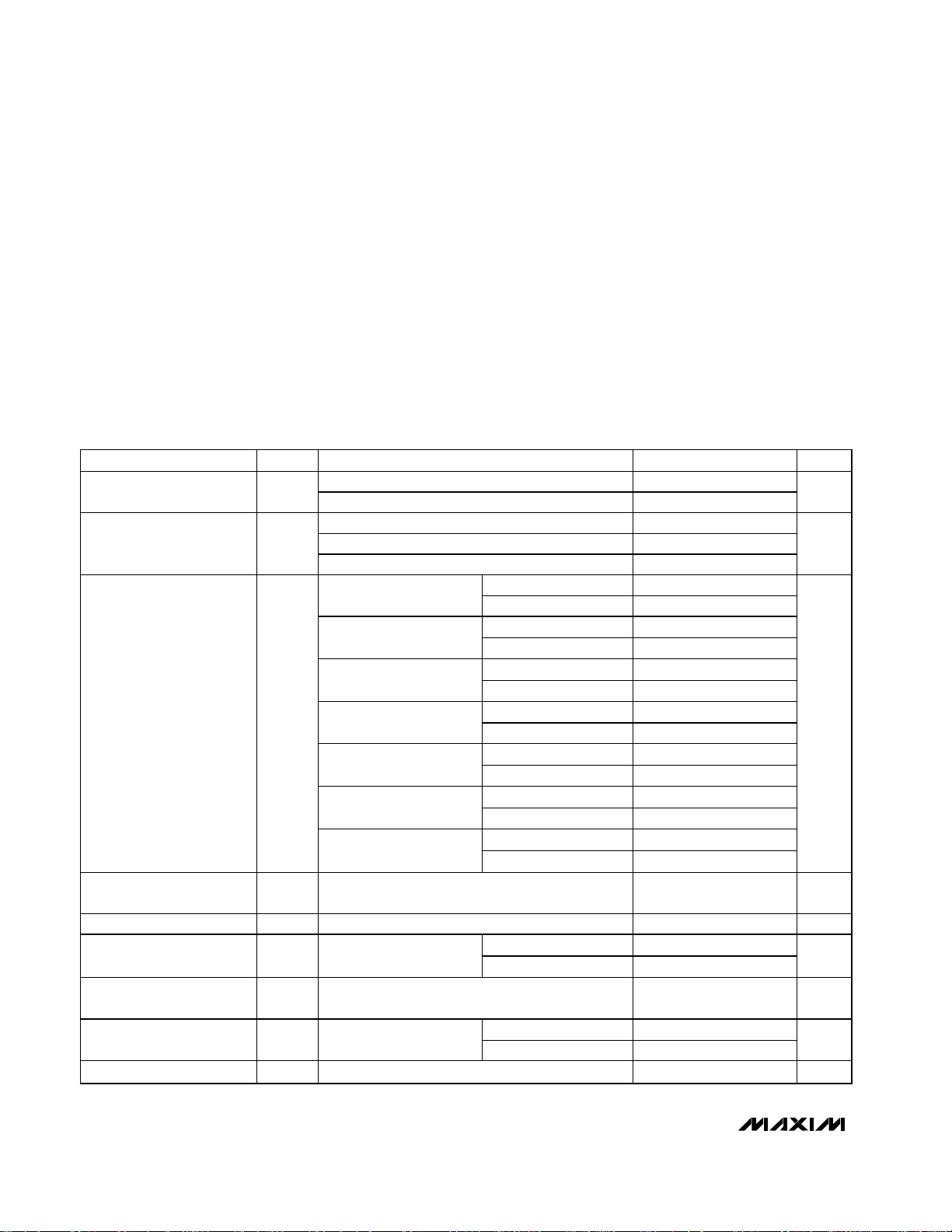
ABSOLUTE MAXIMUM RATINGS
ELECTRICAL CHARACTERISTICS
(VCC= +4.25V to +5.5V for L/M versions, VCC= +2.55V to +3.6V for the T/S/R versions, VCC= +2.1V to +2.75V for the Z/Y versions.
T
A
= -40°C to +125°C, unless otherwise specified. Typical values are at TA= +25°C.) (Note 1)
Stresses beyond those listed under “Absolute Maximum Ratings” may cause permanent damage to the device. These are stress ratings only, and functional
operation of the device at these or any other conditions beyond those indicated in the operational sections of the specifications is not implied. Exposure to
absolute maximum rating conditions for extended periods may affect device reliability.
VCC........................................................................-0.3V to +6.0V
Open-Drain RESET, WDO, PFO ...........................-0.3V to +6.0V
Push-Pull RESET, RESET, WDO, PFO ........-0.3V to (V
CC
+ 0.3V)
MR, WDI, PFI, RST_IN1, RST_IN2 ..............-0.3V to (V
CC
+ 0.3V)
Input Current (V
CC
).............................................................20mA
Output Current (RESET, RESET, PFO, WDO) .....................20mA
Continuous Power Dissipation (T
A
= +70°C)
8-Pin SOT23 (derate 8.9mW/°C above +70°C)............714mW
Operating Temperature Range .........................-40°C to +125°C
Junction Temperature......................................................+150°C
Storage Temperature Range .............................-65°C to +150°C
Lead Temperature (soldering, 10s) .................................+300°C
PARAMETER SYMBOL CONDITIONS MIN TYP MAX UNITS
Operating Voltage Range V
Supply Current
MR Unconnected
VCC Reset Threshold
falling)
(V
CC
I
CC
V
Reset Threshold
Temperature Coefficient
VCC to Reset Output Delay VCC falling at 10mV/µs 12 µs
Reset Timeout Period t
VCC Falling to WDO Delay
PFI, RST_IN1, RST_IN2
Threshold
PFI Hysteresis 6mV
∆V
RP
TA = 0°C to +125°C 1.0 5.5
CC
TA = -40°C to +125°C 1.2 5.5
VCC < 5.5V, no load 12 25
VCC < 3.6V, no load 9 20
VCC < 3.6V, no load (MAX6708 only) 6 20
MAX670_L/MAX670_AL
M AX 670_M /M AX 670_AM
MAX670_T/MAX670_AT
MAX670_S/MAX670_AS
TH
MAX670_R/MAX670_AR
MAX670_Z/MAX670_AZ
MAX670_Y/MAX670_AY
TH
M AX 6701( A) /M AX 6702( A) /M AX 6703( A) /M AX 6705( A) /
M AX 6706( A) /M AX 6707( A)
= 1.8V to 5.5V
V
C C
TA = -40°C to +85°C 4.50 4.63 4.75
= -40°C to +125°C 4.47 4.78
T
A
TA = -40°C to +85°C 4.25 4.38 4.50
= -40°C to +125°C 4.22 4.53
T
A
TA = -40°C to +85°C 3.00 3.08 3.15
= -40°C to +125°C 2.97 3.17
T
A
TA = -40°C to +85°C 2.85 2.93 3.00
= -40°C to +125°C 2.83 3.02
T
A
TA = -40°C to +85°C 2.55 2.63 2.70
= -40°C to +125°C 2.53 2.72
T
A
TA = -40°C to +85°C 2.25 2.32 2.38
= -40°C to +125°C 2.24 2.40
T
A
TA = -40°C to +85°C 2.12 2.19 2.25
= -40°C to +125°C 2.11 2.27
T
A
TA = -40°C to +85°C 140 200 280
TA = -40°C to +125°C 120 300
TA = -40°C to +85°C 602 618 634
= -40°C to +125°C 593 642
T
A
V
µA
V
60 ppm/°C
ms
5µs
mV
MAX6701–08/MAX6701A–03A/05A–07A
Low-Voltage, SOT23 µP Supervisors with Power-
Fail In/Out, Manual Reset, and Watchdog Timer
_______________________________________________________________________________________ 3
ELECTRICAL CHARACTERISTICS (continued)
(VCC= +4.25V to +5.5V for L/M versions, VCC= +2.55V to +3.6V for the T/S/R versions, VCC= +2.1V to +2.75V for the Z/Y versions.
T
A
= -40°C to +125°C, unless otherwise specified. Typical values are at TA= +25°C.) (Note 1)
Note 1: Over-temperature limits are guaranteed by design and not production tested. Devices are tested at T
A
= +25°C.
Note 2: Guaranteed by design. Not production tested.
PARAMETER SYMBOL CONDITIONS MIN TYP MAX UNITS
PFI, RST_IN1, RST_IN2
Leakage Current
PFI to PFO Delay t
MR Input Voltage
(Note 2)
PF
V
IL
V
IH
TA = -40°C to +85°C
T
= -40°C to +125°C
A
-50
-200
0.7 x V
+50
+200
nA
1µs
0.3 x V
CC
CC
V
MR Minimum Input Pulse 1µs
MR Glitch Rejection 100 ns
MR to Reset Delay t
VCC Rising to WDO Delay
MD
MAX6701(A)/MAX6702(A)/MAX6703(A)/
MAX6705(A)/MAX6706(A)/MAX6707(A)
200 ns
100 ns
MR Pullup Resistance 25 50 75 kΩ
Watchdog Timeout Period t
WDI Pulse Width t
WDI Input Voltage
WDI Input Current I
RESET, WDO Output Low
(Push-Pull or Open Drain)
PFO Output Low
(Push-Pull or Open Drain)
RESET, WDO, PFO Output
High (Push-Pull Only)
WDI
V
V
WDI
V
V
V
WD
OH
TA = -40°C to +85°C 1.12 1.6 2.4
TA = -40°C to +125°C 0.96 2.52
(Note 2) 50 ns
IL
IH
OL
OL
WDI = 0V or V
VCC ≥ 1.0V, I
(T
= 0°C to +125°C)
A
VCC ≥ 1.2V, I
V
≥ 2.55V , I
C C
V
≥ 4.25V , I
C C
V
≥ 1.80V , I
C C
V
≥ 2.55V , I
C C
V
≥ 4.25V , I
C C
V
≥ 2.7V , I
C C
V
≥ 4.75V , I
C C
CC
= 50µA, output asserted
SINK
= 100µA, output asserted 0.3
SINK
= 1.2m A, outp ut asser ted 0.3
S IN K
= 3.2m A, outp ut asser ted 0.4
S IN K
= 200µA, outp ut asser ted 0.3
S IN K
= 1.2m A, outp ut asser ted 0.3
S IN K
= 3.2m A, outp ut asser ted 0.4
S IN K
= 500µA, outp ut not asser ted 0.8 x V
S OU RC E
= 800µA, outp ut not asser ted 0.8 x V
S OU RC E
0.7 x V
CC
-1 +1 µA
CC
CC
0.3 x V
0.3
CC
s
V
V
V
V
RESET, WDO, PFO Output
Open-Drain Leakage
I
LKG
VCC > VTH, output not asserted 1.0 µA
Current
RESET Output High
(Push-Pull Only)
RESET Output Low
(Push-Pull Only)
VCC ≥ 1.0V, I
(T
= 0°C to +125°C)
A
V
OH
VCC ≥ 1.2V, I
VCC ≥ 2.55V, I
VCC ≥ 4.25V, I
OL
VCC ≥ 2.7V, I
VCC ≥ 4.75V, I
V
= 1µA, reset asserted
SOURCE
= 50µA, reset asserted 0.8 x V
SOURCE
= 500µA, reset asserted 0.8 x V
SOURCE
= 800µA, reset asserted 0.8 x V
SOURCE
= 1.2mA, reset not asserted 0.3
SINK
= 3.2mA, reset not asserted 0.4
SINK
0.8 x V
CC
CC
CC
CC
V
V
MAX6701–08/MAX6701A–03A/05A–07A
Low-Voltage, SOT23 µP Supervisors with PowerFail In/Out, Manual Reset, and Watchdog Timer
4 _______________________________________________________________________________________
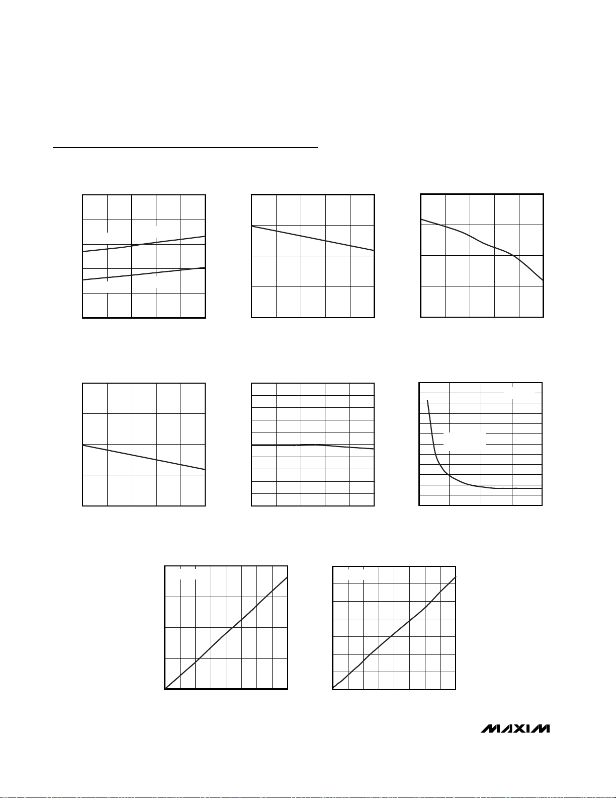
Typical Operating Characteristics
(TA = +25°C, unless otherwise noted.)
0
4
12
8
16
20
-40 10-15 35 60 85
SUPPLY CURRENT vs. TEMPERATURE
MAX6701 toc01
TEMPERATURE (°C)
SUPPLY CURRENT (µA)
VCC = 5V
VCC = 3.3V
MAX6705(A)
MAX6708
210
205
200
195
190
-40 10-15 35 60 85
RESET TIMEOUT PERIOD
vs. TEMPERATURE
MAX6701 toc02
TEMPERATURE (°C)
RESET TIMEOUT PERIOD (ms)
20
15
10
5
0
-40 10-15 356085
VCC TO RESET OUTPUT DELAY
vs. TEMPERATURE
MAX6701 toc03
TEMPERATURE (°C)
V
CC
TO RESET OUTPUT DELAY (µs)
1.70
1.65
1.60
1.55
1.50
-40 10-15 35 60 85
WATCHDOG TIMEOUT PERIOD
vs. TEMPERATURE
MAX6701 toc04
TEMPERATURE (°C)
WATCHDOG TIMEOUT PERIOD (s)
0.95
0.98
0.97
0.96
0.99
1.00
1.01
1.02
1.03
1.04
1.05
-40 10-15 35 60 85
NORMALIZED RESET THRESHOLD
vs. TEMPERATURE
MAX6701 toc05
TEMPERATURE (°C)
NORMALIZED RESET THRESOLD
0 40 80 120 160
MAXIMUM VCC TRANSIENT DURATION
vs. RESET THRESHOLD OVERDRIVE
MAX6701 toc06
RESET THRESHOLD OVERDRIVE (mV)
MAXIMUM TRANSIENT DURATION (µs)
0
10
20
30
40
50
60
MAX670_Y
RESET OCCURS
ABOVE LINE
0
25
50
75
100
0 800 1600 2400400 1200 2000 2800 3200
OUTPUT VOLTAGE LOW
vs. SINK CURRENT
MAX6701 toc07
SINK CURRENT (µA)
V
OL
(mV)
VCC ≥ 4.25V
0
50
150
100
250
300
200
350
0 800 1200400 1600 2000 2400 2800 3200
VCC - VOH vs. SOURCE CURRENT
MAX6701 toc08
SOURCE CURRENT (µA)
V
CC
- V
OH
(mV)
VCC ≥ 4.25V
MAX6701–08/MAX6701A–03A/05A–07A
Low-Voltage, SOT23 µP Supervisors with Power-
Fail In/Out, Manual Reset, and Watchdog Timer
_______________________________________________________________________________________ 5
Pin Description
PIN
MAX6701(A)
MAX6702(A)
MAX6703(A)
11 11MR
22 22V
3 3 3 3 GND Ground
— 4 4 4 PFI
— 555PFO
66 6— WDI
MAX6704
MAX6705(A)
MAX6706(A)
MAX6707(A)
MAX6708
NAME FUNCTION
CC
Active-Low, Manual Reset Input, Internal 50kΩ Pullup to V
Pull low to force a reset. Reset remains active as long as MR is
low and the reset timeout period after MR goes high. Leave
unconnected or connect to V
when MR is low ( M AX 6701( A) /M AX 6702( A) /M AX 6703( A) /
M AX 6705( A) / M AX 6706( A) /M AX 6707( A) onl y) .
S up p l y V ol tag e for M AX 6701–M AX 6708 and Inp ut for P r i m ar y
Reset Thr eshol d M oni tor . P ush- p ul l outp uts ar e p ow er ed b y V
Power-Fail Voltage Monitor Input. High-impedance input for
internal power-fail comparator. Connect this pin to an external
resistive-divider network to set the reset threshold voltage;
0.62V (typ) threshold. Connect to GND or V
Power-Fail Monitor Output. Open drain or push-pull active low.
PFO goes low when PFI is less than 0.62V.
Watchd og Inp ut. If WD I r em ai ns hi g h or l ow for l ong er than the
w atchd og ti m eout p er i od , the i nter nal w atchd og ti m er r uns out and
WDO i s asser ted . WDO i s asser ted l ow after each w atchd og
over fl ow and r em ai ns l ow unti l the w atchd og ti m er i s cl ear ed ( the
r eset outp ut i s not affected ) . The i nter nal w atchd og ti m er cl ear s
w henever a V
r eset i s asser ted , or WD I sees a r i si ng or fal l i ng ed g e. The
w atchd og ti m er r em ai ns cl ear ed unti l the r eset outp ut i s
d easser ted . On the M AX 6704, RES ET p ul se asser ts for the r eset
ti m eout p er i od after each w atchd og ti m eout over fl ow . The
w atchd og ti m er cannot b e d i sab l ed .
/RS T_IN 1/RS T_IN 2 r eset i s a sser ted , the m anual
C C
if unused. WDO deasserts
CC
when not used.
CC
CC
.
C C
.
—— — 6 N.C. No Connection. Not internally connected.
Acti ve- Low Reset Outp ut ( Op en D r ai n or P ush- P ul l ) . RES ET
77 77RESET
chang es fr om hi g h to l ow w hen the V
sel ected r eset thr eshol d ( or RS T_IN 1/ RS T_IN 2 for the
M AX 6701( A) /M AX 6702( A) /M AX 6703( A) , MR i s p ul l ed l ow , or the
w atchd og tr i g g er s a r eset ( M AX 6704 onl y) . RES ET r em ai ns l ow for
the r eset ti m eout p er i od after the r eset cond i ti ons ar e ter m i nated .
i np ut d r op s b el ow the
C C

Detailed Description
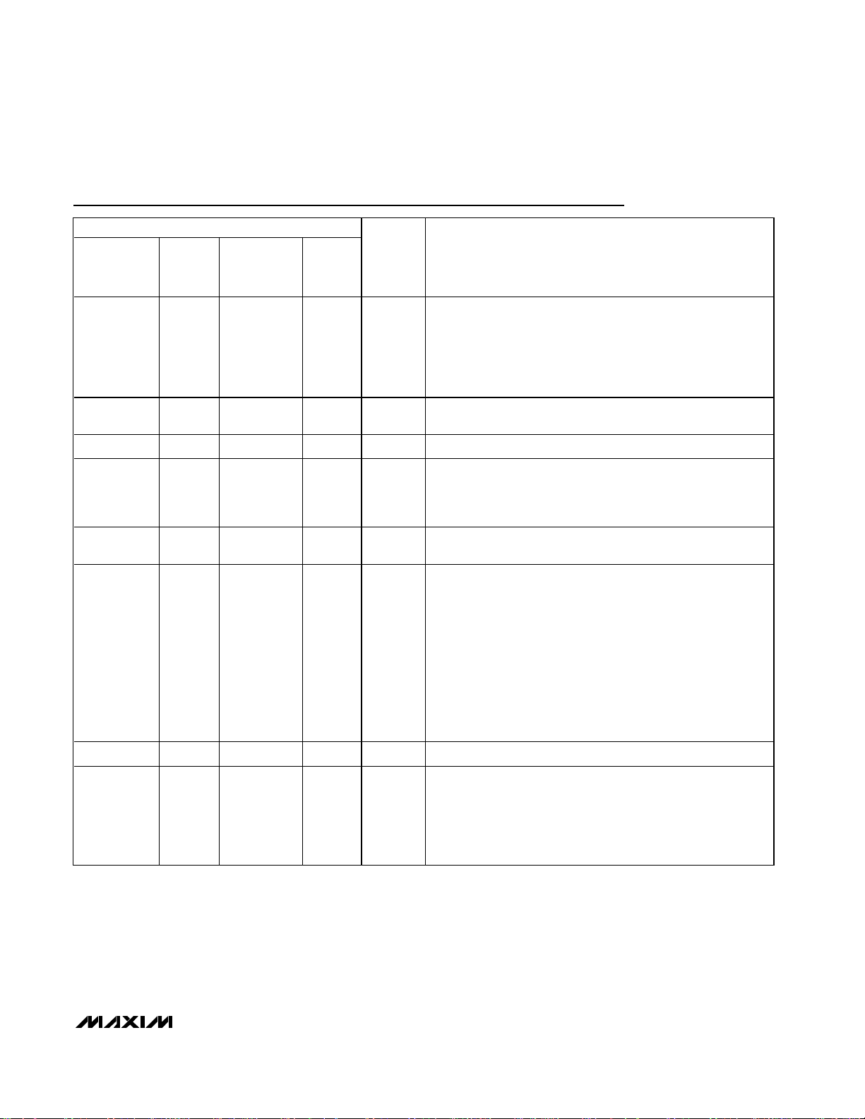
Figures 1, 2, and 3 are functional diagrams for the
MAX6705(A)/MAX6706(A)/MAX6707(A), MAX6704/
MAX6708, and MAX6701(A)/ MAX6702(A)/MAX6703(A),
respectively.
Reset Output
A microprocessor’s (µP’s) reset input starts the µP in a
known state. The MAX6701–MAX6708 assert reset during power-up and prevent code execution errors during
power-down or brownout conditions.
On power-up, once VCCreaches 1V, RESET is a guaranteed logic low of 0.4V or less. As VCCrises, RESET
stays low. After VCC, RST_IN1, or RST_IN2 rise above
the reset threshold, an internal timer holds RESET low
for about 200ms. RESET pulses low whenever VCCdips
below the reset threshold, including brownout conditions. If a brownout occurs in the middle of a previously
initiated reset pulse, the pulse continues for at least
another 140ms. On power-down, once VCCfalls below
the reset threshold, RESET stays low and is guaranteed
to be 0.4V or less, until VCCdrops below 1V.
The MAX6702(A)/MAX6704/MAX6706(A)/MAX6708
active-high RESET output is the complement of the
RESET output, and is guaranteed to be valid with V
CC
down to 1V.
MAX6701–08/MAX6701A–03A/05A–07A
Low-Voltage, SOT23 µP Supervisors with PowerFail In/Out, Manual Reset, and Watchdog Timer
6 _______________________________________________________________________________________
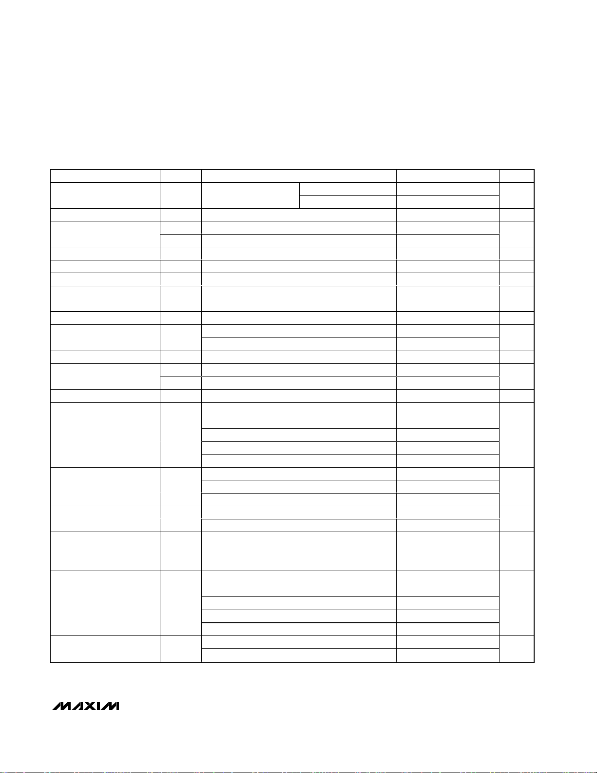
Pin Description (continued)
*RESET active-high for the MAX6702(A)/MAX6706(A).
PIN
MAX6701(A)
MAX6702(A)
MAX6703(A)
8 — 8 — WDO
7* 8 7* 8 RESET
4 ———RST_IN1
MAX6704
MAX6705(A)
MAX6706(A)
MAX6707(A)
MAX6708
NAME FUNCTION
Active-Low Watchdog Output (Open Drain or Push-Pull). WDO
is asserted whenever the watchdog times out and V
reset inputs are below their respective thresholds. WDO
deasserts after a valid WDI transition without a reset timeout
period. In the A versions, WDO deasserts without a timeout
delay when V
threshold. Pull MR low to assert WDO (MAX6701/MAX6702/
MAX6703/MAX6705/MAX6706/MAX6707 only). Pull MR low to
deassert WDO (MAX6701(A)/MAX6702(A)/MAX6703(A)/
MAX6705(A)/MAX6706(A)MAX6707(A) only).
Active-High Reset Output (Push-Pull). RESET changes from low
to high when the V
threshold (or RST_IN1/RST_IN2 for MAX6701(A)/MAX6702(A)/
MAX6703(A), MR is pulled low, or the watchdog triggers a
reset (MAX6704 only). RESET remains high for the reset
timeout period after the reset conditions are terminated.
Input for User-Adjustable V
for second internal reset comparator. Connect this pin to an
external resistive-divider network to set the reset threshold
voltage; 0.62V (typ) threshold. Connect to V
Reset is asserted when either V
below threshold.
, RST_IN1, and RST_IN2 rises above its
CC
input drops below the selected reset
CC
Monitor. High-impedance input
CC2
, RST_IN1, or RST_IN2 are
CC
or the
CC
when not used.
CC
5 ———RST_IN2
Input for User-Adjustable V
for third internal reset comparator. Connect this pin to an
external resistive-divider network to set the reset threshold
voltage; 0.62V (typ) threshold. Connect to V
Reset is asserted when either V
below threshold.
Monitor. High-impedance input
CC3
CC
when not used.
, RST_IN1, or RST_IN2 are
CC
MAX6701–08/MAX6701A–03A/05A–07A
Low-Voltage, SOT23 µP Supervisors with Power-
Fail In/Out, Manual Reset, and Watchdog Timer
_______________________________________________________________________________________ 7
Figure 2. MAX6704/MAX6708 Functional Diagram
Figure 3. MAX6701(A)/MAX6702(A)/MAX6703(A) Functional
Diagram
WATCHDOG
TIMER
RESET
GENERATOR
V
CC
50kΩ
8
WDO
7
RESET
(RESET)
5
PFO
GND
3
0.62V
( ) ARE FOR MAX6706(A) ONLY.
6
WDI
1
MR
2
V
V
REF
CC
4
PFI
MAX6705(A)
MAX6706(A)
MAX6707(A)
Figure 1. MAX6705(A)/MAX6706(A)/MAX6707(A) Functional
Diagram
t
RP
t
RP
V
CC
0V
RESET
WDO
V
CC
0V
WDI
V
CC
0V
MR
MR EXTERNALLY DRIVEN LOW
V
CC
0V
V
CC
V
TH
V
TH
t
MD
NOTE: THE MAX6706 RESET OUTPUT IS THE INVERSE OF THE RESET SHOWN.
Figure 4. MAX6705/MAX6706/MAX6707
RESET, MR, WDO
,
and WDI Timing
V
CC
V
CC
MAX6704
50kΩ
1
MR
2
V
CC
MAX6708
RESET
GENERATOR
8
7
RESET
RESET
50kΩ
MR
V
CC
V
REF
RST_IN1 RST_IN2
0.62V
( ) ARE FOR MAX6702(A) ONLY.
MAX6703(A)
RESET
GENERATOR
MAX6701(A)
MAX6702(A)
WATCHDOG
TIMER
0.62V
RESET (RESET)
WDO
WDI
WATCHDOG
TIMER
4
PFI
V
REF
0.62V
GND
3
6
WDI
(MAX6704 ONLY)
5
PFO

MAX6701–08/MAX6701A–03A/05A–07A
Low-Voltage, SOT23 µP Supervisors with PowerFail In/Out, Manual Reset, and Watchdog Timer
8 _______________________________________________________________________________________
Standard- vs. A-Version Comparison
The MAX6701/MAX6702/MAX6703/MAX6705/MAX6706/
MAX6707s’ WDO latches low when one of the following
events occurs:
• The watchdog timer times out (1.6s, typ).
• VCC, RST_IN1, or RST_IN2 is below its reset threshold.
• MR is pulled low.
• WDO only deasserts with a valid WDI transition.
TheMAX6701(A)/MAX6702(A)/MAX6703(A)/MAX6705(A)/
MAX6706(A)/MAX6707(A)s’ WDO asserts when either
VCC, RST_IN1, or RST_IN2 is below its reset threshold.
WDO deasserts without a timeout delay when the
undervoltage situation has expired. WDO is latched low
when the watchdog timer elapses without seeing a WDI
transition. WDO deasserts with a valid WDI transition
OR by pulling MR low.
See Figures 4 and 5 for standard-version timing. See
Figures 6 and 7 for A-version timing.
Watchdog Timer
The MAX6701–MAX6707 watchdog circuit monitors the
µP’s activity. If the µP does not toggle the WDI within 1.6s,
WDO goes low. When RESET is asserted, the watchdog
timer stays cleared and does not count. As soon as reset
is released, the timer starts counting. WDO deasserts
after a valid transition is detected at WDI. Pulses as short
as 50ns can be detected.
Typically, WDO is connected to the NMI input of a µP.
When VCC, RST_IN1, or RST_IN2 drop below the reset
threshold, WDO goes low whether or not the watchdog
timer has timed out. Normally this would trigger an NMI,
but RESET goes low simultaneously, and thus overrides
the NMI.
The MAX6704 watchdog circuit does not have an independent watchdog output (WDO). If the µP does not
toggle the watchdog input within 1.6s, the MAX6704
asserts a reset output pulse for the reset timeout period.
Manual Reset
The manual reset input (MR) allows reset to be triggered by a pushbutton switch. The switch is effectively
debounced by the reset pulse width. MR is CMOS logic
compatible, so it can be driven by an external logic
line. MR can be used to force a watchdog timeout to
generate a reset pulse in the MAX6701(A)/MAX6702(A)/
MAX6703(A)/MAX6705(A)/MAX6706(A)/MAX6707(A) by
connecting WDO to MR.
Power-Fail Comparator
The uncommitted power-fail comparator can be used
for various purposes because its noninverting input and
output are externally available. The inverting input is
internally connected to a 0.62V reference. To build an
early warning circuit for power failure, connect the PFI
pin to a voltage-divider (see Typical Operating Circuit).
Choose the voltage-divider ratio so that the voltage at
PFI falls below 0.62V just before the regulator drops
out. Use PFO to interrupt the µP so it can prepare for an
orderly power-down. The low-input current at this pin
allows for large resistor values in the divider.
t
WD
t
WD
+5V
0V
WDI
+5V
0V
WDO
+5V
0V
RESET
+5V
0V
(RESET)
t
RP
RESET EXTERNALLY
TRIGGERED BY MR
+5V
0V
MR
( ) ARE FOR MAX6702/MAX6706 ONLY.
t
WDI
t
RP
t
RP
+5V
0V
RESET
WDO
+5V
0V
MR
t
MR
+5V
0V
V
CC
V
TH
V
TH
t
MD
Figure 5. MAX6701/MAX6702/MAX6703/MAX6705/MAX6706/
MAX6707 Watchdog
Figure 6. MAX6701(A)/MAX6702(A)/MAX6703(A)/MAX6705(A)/
MAX6706(A)/MAX6707(A) RESET, MR, and WDO Timing with
WDI Three-Stated

Reset Input
The MAX6701(A)/MAX6702(A)/MAX6703(A) include two
adjustable reset inputs for monitoring up to a total of
three system voltages (including V
CC
). The thresholds
for the monitored RST_IN supplies are externally set
with resistor-divider networks (Figure 8). The reset output is asserted if any of the monitored supplies (VCC,
RST_IN1, or RST_IN2) go below its specified threshold
and remains asserted for the reset timeout period after
all supplies are above their thresholds.
Applications Information
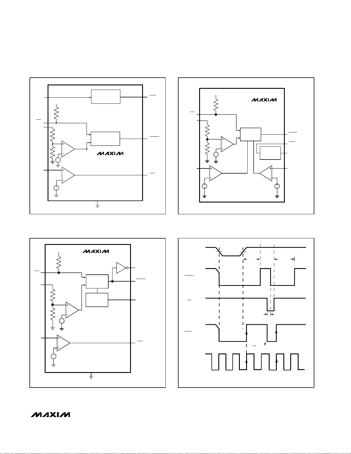
Ensuring a Valid
RESET
Output Down to VCC= 0
When VCCfalls below 1V, the MAX6701–MAX6708
RESET output no longer sinks current—it becomes an
open circuit. High-impedance CMOS logic inputs can
drift to undetermined voltages if left undriven. If a pulldown resistor is added to the RESET pin as shown in
Figure 9, any stray charge or leakage currents are
drained to ground, holding RESET low. A resistor value
(R1) is not critical; 100kΩ is large enough not to load
RESET and small enough to pull RESET to ground. This
application works for push-pull output only (not for
open-drain resets).
Monitoring Other System Voltages
Other systems can be monitored by connecting a voltage-divider to PFI and adjusting the ratio appropriately.
In noisy systems, a capacitor between PFI and GND
reduces the power-fail circuit’s sensitivity to high-frequency noise on the line being monitored. Reset can
be asserted on other voltages in addition to the V
CC
supply line. Connect PFO to MR to initiate a reset output pulse when PFI drops below 0.62V. Figure 10
shows the MAX6704–MAX6708 configured to assert a
reset output when the secondary supply falls below the
reset threshold.
Generating a Reset
from Watchdog Overflow
Connect WDO to MR to force a watchdog timeout to generate a reset pulse for only the reset timeout period on the
MAX6701(A)/MAX6702(A)/MAX6703(A)/MAX6705(A)/
MAX6706(A)/MAX6707(A). When the MAX6704 watchdog times out, reset outputs are automatically asserted
(no external connections required). For the MAX6701/
MAX6702/MAX6703/MAX6705/MAX6706/MAX6707 non-A
versions, do not connect WDO to MR; this creates a
locked condition.
MAX6701–08/MAX6701A–03A/05A–07A
Low-Voltage, SOT23 µP Supervisors with Power-
Fail In/Out, Manual Reset, and Watchdog Timer
_______________________________________________________________________________________ 9
Figure 7. MAX6701(A)/MAX6702(A)/MAX6703(A)/MAX6705(A)/
MAX6706(A)/MAX6707(A) Watchdog Timing
R1
R2
0.62V
PFI, RST_IN1, OR RST_IN2
V
EXTERNAL
0.62
R1 = R2 x
(
V
EXT-TH
- 1
)
R2
V
EXT-TH
= (1 +
R1
)
x 0.62V
WHERE V
EXT-TH
IS THE EXTERNAL VOLTAGE TRIP LEVEL.
MAX6701(A)–
MAX6708
Figure 8. Calculating Adjustable Voltage Thresholds
t
WDI
+5V
WDI
0V
+5V
WDO
0V
+5V
RESET
0V
+5V
(RESET)
0V
+5V
MR
0V
( ) ARE FOR MAX6702(A)/MAX6706(A) ONLY.
t
WD
t
WD
t
WD
t
RP
MAX6701–08/MAX6701A–03A/05A–07A
Low-Voltage, SOT23 µP Supervisors with PowerFail In/Out, Manual Reset, and Watchdog Timer
10 ______________________________________________________________________________________
Threshold Suffix Guide
Bold indicates standard version.
R1 (100kΩ)
RESET
MAX6701(A)
MAX6704
MAX6705(A)
MAX6708
Figure 9.
RESET
Valid to Ground Circuit
V
CC
PFI
MR
PFO
RESET
0.9V
3.3V
MAX6704–
MAX6708
I/O
SUPPLY
CORE
SUPPLY
µP
RESET
(RESET)
() ARE FOR MAX6704/MAX6706(A)/MAX6708 ONLY.
Figure 10. Monitoring Other System Voltages
Selector Guide
PP = push-pull, OD = open drain.
*
WDO
deasserts when MRis pulled low. See the Standard- vs. A-Version Comparison section for the differences on
WDO
.
PART
MAX6701 ✔ ——✔✔ PP — ✔
MAX6701A* ✔ ——✔✔ PP — ✔
MAX6702 — ✔ — ✔✔ PP — ✔
MAX6702A* — ✔ — ✔✔ PP — ✔
MAX6703 —— ✔✔✔ OD — ✔
MAX6703A* ——✔✔✔ OD — ✔
MAX6704 ✔✔— ✔ — ✔ PP —
MAX6705 ✔ ——✔✔ PP ✔ PP —
MAX6705A* ✔ ——✔✔ PP ✔ PP —
MAX6706 — ✔ — ✔✔ PP ✔ PP —
MAX6706A* — ✔ — ✔✔ PP ✔ PP —
MAX6707 —— ✔✔✔ OD ✔ OD —
MAX6707A* ——✔✔✔ OD ✔ OD —
MAX6708 ✔✔———✔ PP —
RESET
PP LOW
SUFFIX
RESET
PP HIGH
RESET
THRESHOLD (V)
RESET
OD-LOW
WDI WDO
L 4.63
M 4.38
T 3.08
S 2.93
R 2.63
Z 2.32
Y 2.19
PFI,
PFO
RST_IN1,
RST_IN2

MAX6701–08/MAX6701A–03A/05A–07A
Low-Voltage, SOT23 µP Supervisors with Power-
Fail In/Out, Manual Reset, and Watchdog Timer
______________________________________________________________________________________ 11
Typical Operating Circuit
Pin Configurations (continued)
Chip Information
TRANSISTOR COUNT: 716
PROCESS: BiCMOS
Ordering Information (continued)
Insert the desired suffix letter (from the Threshold Suffix Guide
table) into the blank to complete the part number. All devices
must be ordered in increments of 2500 pieces. Sample stock is
typically held on standard versions only. Contact factory for
availability.
TOP VIEW
MR
GND
UNREGULATED DC
PUSHBUTTON
1
2
CC
MAX6704
3
4
87RESET
RESETV
WDI
6
PFOPFI
5
MR
CC
GND
SOT23
DC/DC
SWITCH
REGULATOR
V
PFI
MR
CC
MAX6705(A)
MAX6706(A)
MAX6707(A)
RESET
WDI
WDO
PFO
µP
V
CC
RESET
I/O
NMI
INTERRUPT
1
2
87WDO
MAX6705(A)
MAX6706(A)
3
4
MAX6707(A)
6
5
SOT23
( ) ARE FOR MAX6706(A) ONLY.
MAX6702_ KA-T -40°C to +125°C 8 SOT23-8
MAX6702A_ KA-T -40°C to +125°C 8 SOT23-8
MAX6703_ KA-T -40°C to +125°C 8 SOT23-8
MAX6703A_ KA-T -40°C to +125°C 8 SOT23-8
MAX6704_KA-T -40°C to +125°C 8 SOT23-8
MAX6705_KA-T -40°C to +125°C 8 SOT23-8
MAX6705A_KA-T -40°C to +125°C 8 SOT23-8
MAX6706_KA-T -40°C to +125°C 8 SOT23-8
MAX6706A_KA-T -40°C to +125°C 8 SOT23-8
MAX6707_KA-T -40°C to +125°C 8 SOT23-8
MAX6707A_KA-T -40°C to +125°C 8 SOT23-8
MAX6708_KA-T -40°C to +125°C 8 SOT23-8
MR
1
RESET (RESET)V
WDI
PFOPFI
GND
2
CC
MAX6708
3
4
SOT23
PART TEMP RANGE PIN-PACKAGE
87RESET
RESETV
N.C.
6
PFOPFI
5

MAX6701–08/MAX6701A–03A/05A–07A
Low-Voltage, SOT23 µP Supervisors with PowerFail In/Out, Manual Reset, and Watchdog Timer
Maxim cannot assume responsibility for use of any circuitry other than circuitry entirely embodied in a Maxim product. No circuit patent licenses are
implied. Maxim reserves the right to change the circuitry and specifications without notice at any time.
12 ____________________Maxim Integrated Products, 120 San Gabriel Drive, Sunnyvale, CA 94086 408-737-7600
© 2003 Maxim Integrated Products Printed USA is a registered trademark of Maxim Integrated Products.
Package Information
(The package drawing(s) in this data sheet may not reflect the most current specifications. For the latest package outline information,
go to www.maxim-ic.com/packages
.)
PIN 1
I.D. DOT
(SEE NOTE 6)
A
SEE DETAIL "A"
b
C
L
C
L
e1
D
C
L
A2
e
C
E
A1
L
C
SEATING PLANE C
E1
SYMBOL
A
C
L
L2
e
e1
0
L
NOTE:
1. ALL DIMENSIONS ARE IN MILLIMETERS.
2. FOOT LENGTH MEASURED FROM LEAD TIP TO UPPER RADIUS OF
HEEL OF THE LEAD PARALLEL TO SEATING PLANE C.
3. PACKAGE OUTLINE EXCLUSIVE OF MOLD FLASH & METAL BURR.
4. PACKAGE OUTLINE INCLUSIVE OF SOLDER PLATING.
5. COPLANARITY 4 MILS. MAX.
6. PIN 1 I.D. DOT IS 0.3 MM MIN. LOCATED ABOVE PIN 1.
7. SOLDER THICKNESS MEASURED AT FLAT SECTION OF LEAD
BETWEEN 0.08mm AND 0.15mm FROM LEAD TIP.
8. MEETS JEDEC MO178.
PROPRIETARY INFORMATION
TITLE:
PACKAGE OUTLINE, SOT-23, 8L BODY
DETAIL "A"
MIN
0.90
0.00A1
0.90A2
0.28b
0.09
2.80D
1.50E1
0.30
0.25 BSC.
0.65 BSC.
1.95 REF.
0
L2
0
21-0078
MAX
1.45
0.15
1.30
0.45
0.20
3.00
3.002.60E
1.75
0.60
8
GAUGE PLANE
SOT23, 8L .EPS
REV.DOCUMENT CONTROL NO.APPROVAL
1
D
1
 Loading...