

Page 1
General Description
The MAX6691 four-channel thermistor temperature-topulse-width converter measures the temperatures of up
to four thermistors and converts them to a series of output pulses whose widths are related to the thermistors’
temperatures. Each of the four thermistors and an
external fixed resistor (R
EXT
) form a voltage-divider that
is driven by the MAX6691’s internal voltage reference
(V
REF
). V
REF
and the voltage across R
EXT
are mea-
sured and converted to a pulse.
The MAX6691 has a single open-drain I/O pin that can
be readily connected to a variety of microcontrollers.
The microcontroller initiates a conversion by pulling the
I/O pin low and releasing it. When conversion is done,
the MAX6691 signals the end of conversion by pulling
the I/O pin low once again. The pulse corresponding to
the first thermistor is sent immediately after the release
of the I/O pin.
The on-chip power-management circuitry reduces the
average thermistor current to minimize errors due to
thermistor self-heating. Between conversions, the
MAX6691 falls into a 10µA (max) sleep mode, where
the voltage reference is disabled and the supply current is at its minimum.
The MAX6691 is available in a 10-pin µMAX package
and is specified from -55°C to +125°C temperature
range.
Applications
HVAC
Home Appliances
Medical Devices
Features
♦ Simple Single-Wire Interface
♦ Measures Up to Four Thermistor Temperatures
♦ Low-Average Thermistor Current Minimizes Self-
Heating Errors
♦ Internal Voltage Reference Isolates Thermistor
from Power-Supply Noise
♦ Accommodates Any Thermistor Temperature
Range
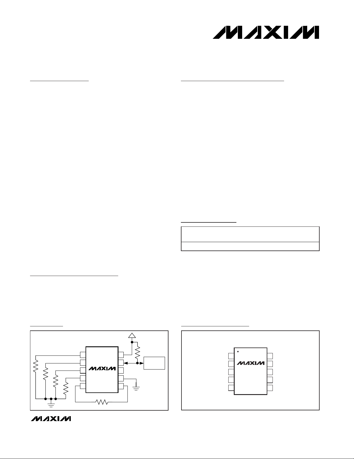
MAX6691
Four-Channel Thermistor Temperature-to-Pulse-
Width Converter
________________________________________________________________ Maxim Integrated Products 1
1
2
3
4
5
10
9
8
7
6
V
CC
I/O
N.C.
GNDT4
T3
T2
T1
MAX6691
µMAX
TOP VIEW
R+R-
Pin Configuration
1
2
3
4
5
10
9
8
7
6
V
CC
I/O
N.C.
GND
T4
T3
T2
T1
MAX6691
TOP VIEW
R+
R-
T4
T3
T2
T1
MICRO-
CONTROLLER
10kΩ
V
CC
R
EXT
Typical Application Circuit
19-2304; Rev 1; 2/07
For pricing, delivery, and ordering information, please contact Maxim/Dallas Direct! at
1-888-629-4642, or visit Maxim’s website at www.maxim-ic.com.
Ordering Information
PART
TEMP RANGE
PIN-
PKG
CODE
MAX6691MUB
10 µMAX
U10-2
PACKAGE
-55°C to +125°C
Page 2
MAX6691
Four-Channel Thermistor Temperature-to-PulseWidth Converter
2 _______________________________________________________________________________________
ABSOLUTE MAXIMUM RATINGS
Stresses beyond those listed under “Absolute Maximum Ratings” may cause permanent damage to the device. These are stress ratings only, and functional
operation of the device at these or any other conditions beyond those indicated in the operational sections of the specifications is not implied. Exposure to
absolute maximum rating conditions for extended periods may affect device reliability.
Note 1: Specification limits over temperature are guaranteed by design, not production tested.
VCCto GND...........................................................-0.3V to +6.0V
All Other Pins to GND.................................-0.3V to (V
CC
+ 0.3V)
I/O, R+, R-, T1–T4 Current................................................±20mA
ESD Protection (Human Body Model) .............................±2000V
Continuous Power Dissipation (T
A
= +70°C)
10-Pin µMAX (derate 5.6mW/°C above +70°C) ........444.4mW
Operating Temperature Range .........................-55°C to +125°C
Junction Temperature......................................................+150°C
Storage Temperature Range .............................-65°C to +150°C
Lead Temperature (soldering, 10s) .................................+300°C
ELECTRICAL CHARACTERISTICS
(VCC= 3.0V to 5.5V, TA= -55°C to +125°C, unless otherwise noted. Typical values are specified at VCC= 3.3V and TA= +25°C.) (Note1)
PARAMETER
CONDITIONS
UNITS
TA = +25°C, VCC = 3.3V 0.5
T
HIGH/TLOW
Accuracy V
REXT
TA = T
MIN
to T
MAX
1.0
% FS
Supply Voltage Range V
CC
3.0 5.5 V
Supply Current I
CC
During conversion, no load
µA
Sleep-Mode Supply Current
3.5 10 µA
Input Leakage Current
1.0 µA
Reference Voltage Output V
REF
I
REF
= 1mA, TA = +25°C
V
Reference Load Regulation 0 < I
REF
< 2mA 0.1 0.2 %
Reference Supply Rejection 0.2 %
Logic Input Low Voltage V
IL
0.3
✕
V
Logic Input High Voltage V
IH
0.7
✕
V
TIMING CHARACTERISTICS
(VCC= 3.0V to 5.5V, TA= -55°C to +125°C, unless otherwise noted. Typical values are specified at VCC= 3.3V and TA= +25°C.)
(Figure 1) (Note1)
PARAMETER
CONDITIONS
UNITS
Glitch Immunity on I/O Input
ns
Conversion Time t
CONV
86
ms
Nominal Pulse Width t
LOW
4.0 4.9 7.5 ms
Start Pulse Width t
START
5µs
Data Ready Pulse Width t
READY
µs
Error Pulse Width t
ERROR
µs
Rise Time t
RISE
CL = 15pF, RL = 10kΩ
ns
Fall Time t
FALL
CL = 15pF, RL = 10kΩ
ns
SYMBOL
I
STANDBY
I
LEAKAGE
MIN TYP MAX
300 600
1.19 1.24 1.32
V
CC
SYMBOL
MIN TYP MAX
103 122 188
103 122 188
500
102 156
600
600
V
CC
Page 3
MAX6691
Four-Channel Thermistor Temperature-to-Pulse-
Width Converter
_______________________________________________________________________________________ 3
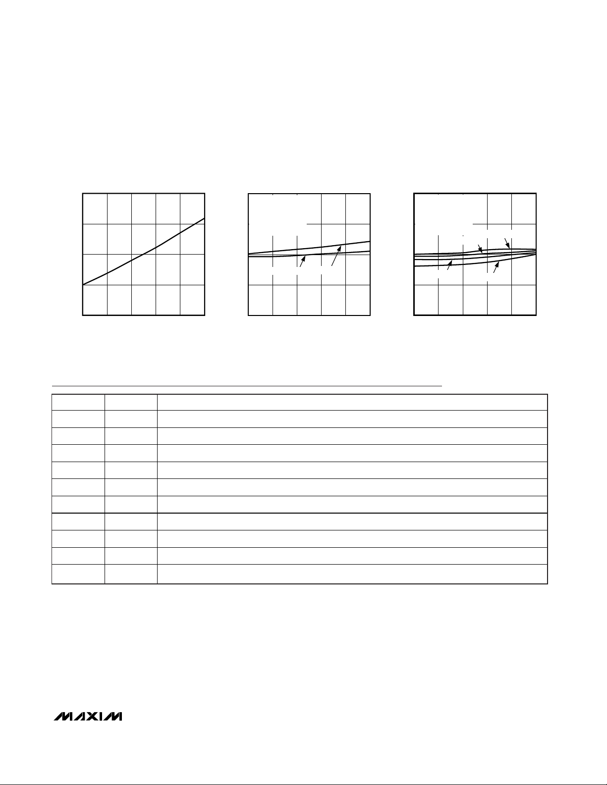
SLEEP-MODE SUPPLY CURRENT
vs. SUPPLY VOLTAGE
MAX6691 toc01
SUPPLY VOLTAGE (V)
SLEEP-MODE SUPPLY CURRENT (µA)
5.04.54.03.5
3.0
3.5
4.0
4.5
2.5
3.0 5.5
T
HIGH/TLOW
ERROR
vs. POWER-SUPPLY NOISE FREQUENCY
MAX6691 toc02
POWER-SUPPLY NOISE FREQUENCY (MHz)
T
HIGH
/T
LOW
FULL-SCALE ERROR (%)
2015105
-0.5
0
0.5
1.0
-1.0
025
VCC = 5.0V
VCC = 3.3V
VIN = SQUARE WAVE
APPLIED TO V
CC
WITH
NO VCC BYPASS
CAPACITOR
V
IN
= 250mV
P-P
T
HIGH/TLOW
ERROR
vs. POWER-SUPPLY NOISE FREQUENCY
MAX6691 toc03
POWER-SUPPLY NOISE FREQUENCY (MHz)
T
HIGH
/T
LOW
FULL-SCALE ERROR (%)
2015105
-0.5
0
0.5
1.0
-1.0
025
TA = +25°C
TA = -55°C
TA = +85°C
TA = +125°C
VIN = SQUARE WAVE
APPLIED TO V
CC
WITH
NO VCC BYPASS
CAPACITOR
V
IN
= 250mV
P-P
__________________________________________Typical Operating Characteristics
(VCC= 5V, R
EXT
= 7.5kΩ, RTH= 12.5kΩ, TA= +25°C, unless otherwise noted.)
PIN NAME FUNCTION
1 T1 Thermistor 1. Connect to external thermistor 1.
2 T2 Thermistor 2. Connect to external thermistor 2.
3 T3 Thermistor 3. Connect to external thermistor 3.
4 T4 Thermistor 4. Connect to external thermistor 4.
5 R- External Resistor Low Side. Connect R
EXT
between R- and R+.
6 R+ Reference Voltage Output. Connect R
EXT
between R- and R+.
7 GND Ground. Ground connection for MAX6691 and ground return for external thermistor(s).
8 N.C. No Connection. Do not make a connection to this pin.
9 I/O I/O Connection to Microcontroller. Connect a 10kΩ pullup resistor from I/O pin to V
CC
.
10 V
CC
Supply Voltage. Bypass VCC to GND with a capacitor of at least 0.1µF.
Pin Description
Page 4
MAX6691
Detailed Description
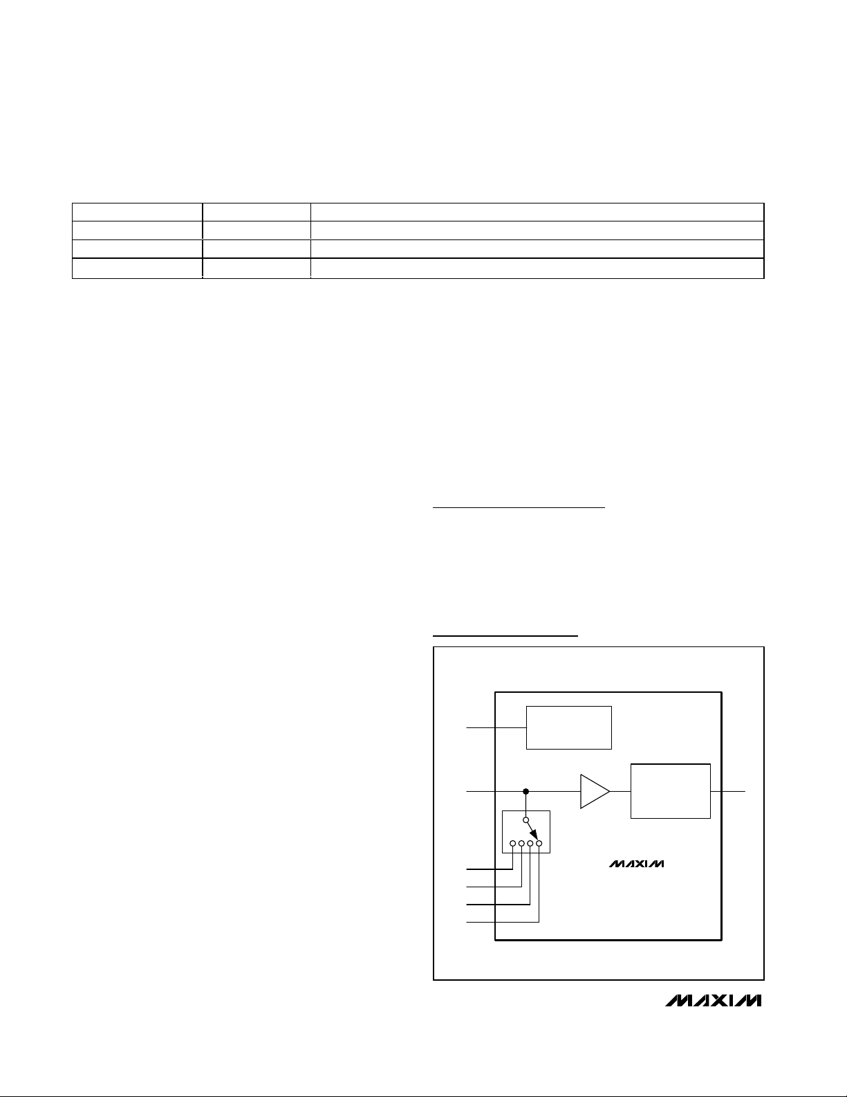
The MAX6691 is an interface circuit that energizes up to
four thermistors and converts their temperatures to a
series of output pulses. The MAX6691 powers the thermistors only when a measurement is being made. This
minimizes the power dissipation in the thermistors, virtually eliminating self-heating, a major component of thermistor error. The simple I/O allows the initiation of
conversion and delivery of output pulses or a single pin.
Temperature Measurement
When it is not performing conversions or transmitting
output pulses, the MAX6691 is in a low-power sleep
mode and the I/O pin is held at VCCby the external
pullup resistor (typically 10kΩ). To initiate measurement
of up to four thermistor temperatures, the external
microcontroller pulls the I/O pin low for at least 5µs
(Figure 1). When the microcontroller releases the I/O
pin, the MAX6691 applies the reference voltage (V
REF
)
to the external resistor (R
EXT
), which is connected
sequentially to each of the four external thermistors (T1
through T4).
When the measurements are complete (after a period
equal to T
CONV
), the MAX6691 pulls the I/O pin low for
125µs. The I/O pin remains high for a period proportional to the first V
EXT
measurement (corresponding to the
first thermistor). The MAX6691 then pulls the I/O pin low
for a period proportional to V
REF
. Three more high/low
pulse pairs follow, corresponding to T2 through T4,
after which the I/O pin is released.
The relationship between pulse width, R
EXT
, and ther-
mistor resistance (RTH) can be described as:
The relationship between V
EXT
and the temperature of
a thermistor is determined by the values of R
EXT
and
the thermistor’s characteristics. If the relationship
between RTHand the temperature is known, a microcontroller with no on-chip ADC can measure T
HIGH
and
T
LOW
and accurately determine the temperature at the
corresponding thermistor.
For each operation, the MAX6691 generates four pulses on the I/O pin. In the case of an open or short connection on the thermistor, the corresponding pulse
(T
HIGH
) is a short pulse of less than 5% of T
LOW
.
Applications Information
Thermistors and Thermistor Selection
Either NTC or PTC thermistors can be used with the
MAX6691, but NTC thermistors are more commonly
used. NTC thermistors are resistive temperature sensors whose resistance decreases with increasing temperature. They are available in a wide variety of
packages that are useful in difficult applications such
as measurement of air or liquid temperature. Some can
operate over temperature ranges beyond that of most
ICs. The relationship between temperature and resistance in an NTC thermistor is very nonlinear and can be
described by the following approximation:
Where T is absolute temperature, R is the thermistor’s
resistance, and A, B, C are coefficients that vary with
manufacturer and material characteristics. The general
shape of the curve is shown in Figure 2.
1
3
T
C InR=+A B(InR)+ ()
T
T
V
V
.0002 =
R
R+R
HIGH
LOW
EXT
REF
EXT
EXT TH
=− −0 0 0002.
Four-Channel Thermistor Temperature-to-PulseWidth Converter
4 _______________________________________________________________________________________
t
START
CONV REQUEST,
PULLED LOW BY µC
t
READY
DATA READY,
PULLED LOW BY
MAX6691
t
ERROR
THERMISTOR IS
EITHER OPEN OR
SHORT
t
CONV
T
HIGH1
T
HIGH2
T
HIGH4
THERMISTOR 1
DATA
T
LOW
T
LOW
T
LOW
T
LOW
THERMISTOR 2
DATA
THERMISTOR 3
DATA
THERMISTOR 4
DATA
Figure 1. Timing Diagram
Page 5
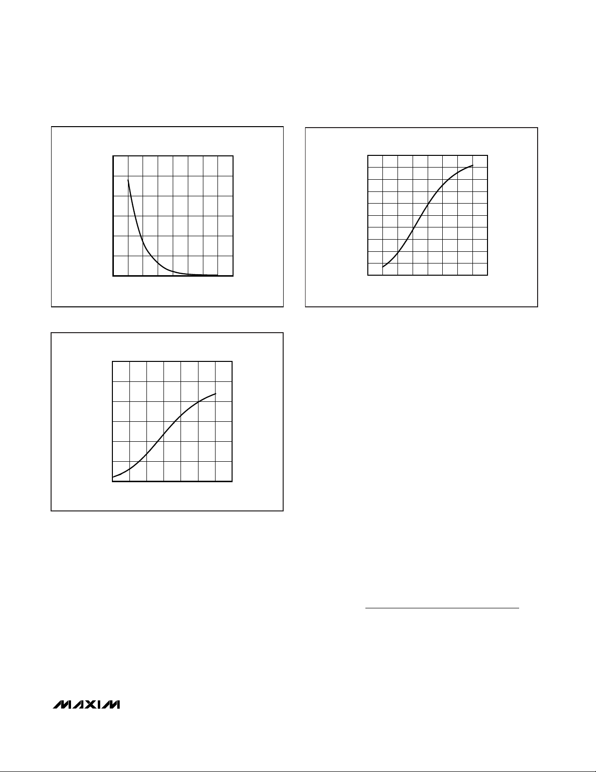
The relationship between temperature and resistance
of an NTC thermistor is highly nonlinear. However, by
connecting the thermistors in series with a properly
chosen resistor (R
EXT
) and using the MAX6691 to measure the voltage across the resistor, a reasonably linear
transfer function can be obtained over a limited temperature range. Linearity improves for smaller temperature
ranges.
Figures 3 and 4 show typical T
HIGH/TLOW
curves for a
standard thermistor in conjunction with values of R
EXT
chosen to optimize linearity over two series resistors
chosen to optimize linearity over two different temperature ranges.
NTC thermistors are often described by the resistance
at +25°C. Therefore, a 10kΩ thermistor has a resistance of 10kΩ at +25°C. When choosing a thermistor,
ensure that the thermistor’s minimum resistance (which
occurs at the maximum expected operating temperature) in series with R
EXT
does not cause the voltage reference output current to exceed about 1mA. Some
standard 10kΩ thermistors with similar characteristics
are listed in Table 1.
Choosing R
EXT
Choose R
EXT
to minimize nonlinearity errors from the
thermistor:
1) Decide on the temperature range of interest (for
example 0°C to +70°C).
2) Find the thermistor values at the limits of the tem-
perature range. R
MIN
is the minimum thermistor
value (at the maximum temperature) and R
MAX
is
the maximum thermistor value (at the minimum temperature). Also find R
MID
, the thermistor resistance
in the middle of the temperature range (+35°C for
the 0°C to +70°C range).
3) Find R
EXT
using the equation below:
Power-Supply Considerations
The MAX6691 accuracy is relatively unaffected by
power-supply coupled noise. In most applications,
R
RR RR
RR R
MIN MAX MIN MAX
MIN MAX MID
EXT
MID
=
R
+
()
−×
+−
2
2
MAX6691
Four-Channel Thermistor Temperature-to-Pulse-
Width Converter
_______________________________________________________________________________________ 5
Figure 2. Thermistor Resistance vs. Temperature
0
20
40
60
80
100
120
-40 0-20 20406080100120
THERMISTOR RESISTANCE
vs. TEMPERATURE
TEMPERATURE (°C)
THERMISTOR RESISTANCE (kΩ)
Figure 3. T
HIGH/TLOW
vs. Temperature, R
EXT
= 5110Ω
T
HIGH/TLOW
vs. TEMPERATURE FOR BETATHERM
10K3A1 THERMISTOR WITH R
EXT
= 5110Ω
TEMPERATURE (°C)
T
HIGH
/T
LOW
12010080604020
0.2
0.4
0.6
0.8
1.0
1.2
0
0 140
Figure 4. T
HIGH/TLOW
vs. Temperature, R
EXT
= 7680Ω
T
HIGH/TLOW
vs. TEMPERATURE FOR BETATHERM
10K3A1 THERMISTOR WITH R
EXT
= 7680Ω
TEMPERATURE (°C)
T
HIGH
/T
LOW
1008040 600 20-20
0.1
0.2
0.3
0.4
0.5
0.6
0.7
0.8
0.9
1.0
0
-40 120
Page 6
MAX6691
bypass VCCto GND by placing a 0.1µF to 1.0µF
ceramic bypass capacitor close to the supply pin of the
devices.
Thermal Considerations
Self-heating degrades the temperature measurement
accuracy of thermistors. The amount of self-heating
depends on the power dissipated and the dissipation
constant of the thermistor. Dissipation constants
depend on the thermistor’s package and can vary considerably.
A typical thermistor might have a dissipation constant
equal to 1mW/°C. For every milliwatt the thermistor dissipates, its temperature rises by 1°C. For example, consider a 10kΩ (at +25°C) NTC thermistor in series with a
5110Ω resistor operating +40°C with a constant 5V
bias. If it is one of the standard thermistors previously
mentioned, its resistance is 5325Ω at this temperature.
The power dissipated in the thermistor is:
(5V)2 (5325Ω) / (5325Ω + 5110Ω)2= 1.22mW
This thermistor therefore has a self-heating error at
+40°C of 1.22°C. Because the MAX6691 uses a small
reference voltage and energizes each thermistor for
only about 25ms per conversion cycle, the self-heating
of the thermistor under the same conditions when used
with the MAX6691 is far less. Assuming one conversion
cycle every 5s, each thermistor is energized only 0.5%
of the time:
(1.22)2 (5325)(0.005) / (5325 + 5110)2= 0.364µW, or
only about 0.00036°C self-heating error.
Chip Information
TRANSISTOR COUNT: 7621
PROCESS: BiCMOS
Four-Channel Thermistor Temperature-to-PulseWidth Converter
6 _______________________________________________________________________________________
Table 1. Standard Thermistors
MANUFACTURER PART WEBSITE
Betatherm 10K3A1 www.betatherm.com/indexna.htm
Dale 1M1002 www.vishay.com/brands/dale/main.html
Thermometrics C100Y103J www.thermometrics.com
Functional Diagram
R+
REFERENCE
R-
T1
T2
T3
T4
VOLTAGE-TO-PWM
CONVERTER
MAX6691
I/O
Page 7
MAX6691
Four-Channel Thermistor Temperature-to-Pulse-
Width Converter
Maxim cannot assume responsibility for use of any circuitry other than circuitry entirely embodied in a Maxim product. No circuit patent licenses are
implied. Maxim reserves the right to change the circuitry and specifications without notice at any time.
Maxim Integrated Products, 120 San Gabriel Drive, Sunnyvale, CA 94086 408-737-7600 _____________________ 7
© 2007 Maxim Integrated Products is a registered trademark of Maxim Integrated Products, Inc.
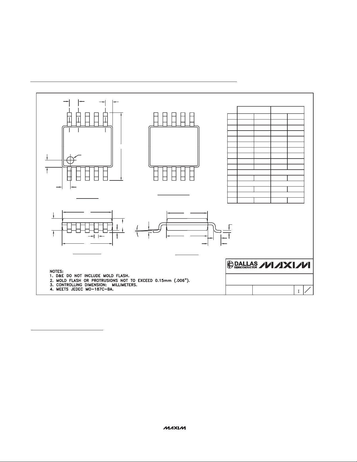
Package Information
10LUMAX.EPS
PACKAGE OUTLINE, 10L uMAX/uSOP
1
1
21-0061
REV.DOCUMENT CONTROL NO.APPROVAL
PROPRIETARY INFORMATION
TITLE:
TOP VIEW
FRONT VIEW
1
0.498 REF
0.0196 REF
S
6°
SIDE VIEW
α
BOTTOM VIEW
0° 0° 6°
0.037 REF
0.0078
MAX
0.006
0.043
0.118
0.120
0.199
0.0275
0.118
0.0106
0.120
0.0197 BSC
INCHES
1
10
L1
0.0035
0.007
e
c
b
0.187
0.0157
0.114
H
L
E2
DIM
0.116
0.114
0.116
0.002
D2
E1
A1
D1
MIN
-A
0.940 REF
0.500 BSC
0.090
0.177
4.75
2.89
0.40
0.200
0.270
5.05
0.70
3.00
MILLIMETERS
0.05
2.89
2.95
2.95
-
MIN
3.00
3.05
0.15
3.05
MAX
1.10
10
0.6±0.1
0.6±0.1
Ø0.50±0.1
H
4X S
e
D2
D1
b
A2
A
E2
E1
L
L1
c
α
GAGE PLANE
A2 0.030 0.037 0.75 0.95
A1
Revision History
Pages changed at Rev 1: 1, 5, 7
 Loading...