

General Description
MAX6685/MAX6686 are dual-output temperature switches
that use an external diode-connected transistor as a sensing element. These devices have two logic outputs (T
HIGH
and T
LOW
). T
HIGH
asserts a logic signal when the remote
temperature crosses the factory-programmed, +120°C, or
+125°C upper trip threshold. T
LOW
is asserted when the
remote temperature exceeds the lower threshold, which is
controlled by pins S1 and S2. The lower thresholds are
available in two ranges in 5°C increments. The two ranges
are +40°C to +80°C and +75°C to +115°C. Hysteresis for
both outputs to be deasserted is typically 5°C.
T
HIGH
is an open-drain, active-low output for both the
MAX6685 and the MAX6686. T
LOW
is a CMOS push-pull,
active-high output for the MAX6685 and is an open-drain,
active-low output for the MAX6686. They are available in
a space-saving 8-pin µMAX package.
Applications
Features
♦ Pin-Programmed Lower Temperature Threshold
from +40°C to +80°C or +75°C to +115°C
(5°C Increments)
♦ Preset Upper Threshold: +120°C or +125°C
♦ Open-Drain, Active-Low Output for Upper
Temperature Alarm
♦ CMOS Push-Pull, Active-High or Open-Drain,
Active-Low Output for Lower Temperature Alarm
♦ 1.5°C Accuracy
♦ 3.0V to 5.5V, 200µA Supply
♦ 8-Pin µMAX Package
MAX6685/MAX6686
Dual-Output Remote-Junction
Temperature Switches
________________________________________________________________ Maxim Integrated Products 1
Ordering Information
MAX6685
C
S
12V
GND
CPU
S1
DXN
S2
3.3V
TO SYSTEM
SHUTDOWN
N
T
LOW
DXP
V
DD
T
HIGH
MAX6686
C
S
GND
CPU
S1
DXN
S2
3.3V
TO SYSTEM
SHUTDOWN
TO CLOCK
THROTTLE
CONTROL
T
LOW
DXP
V
DD
T
HIGH
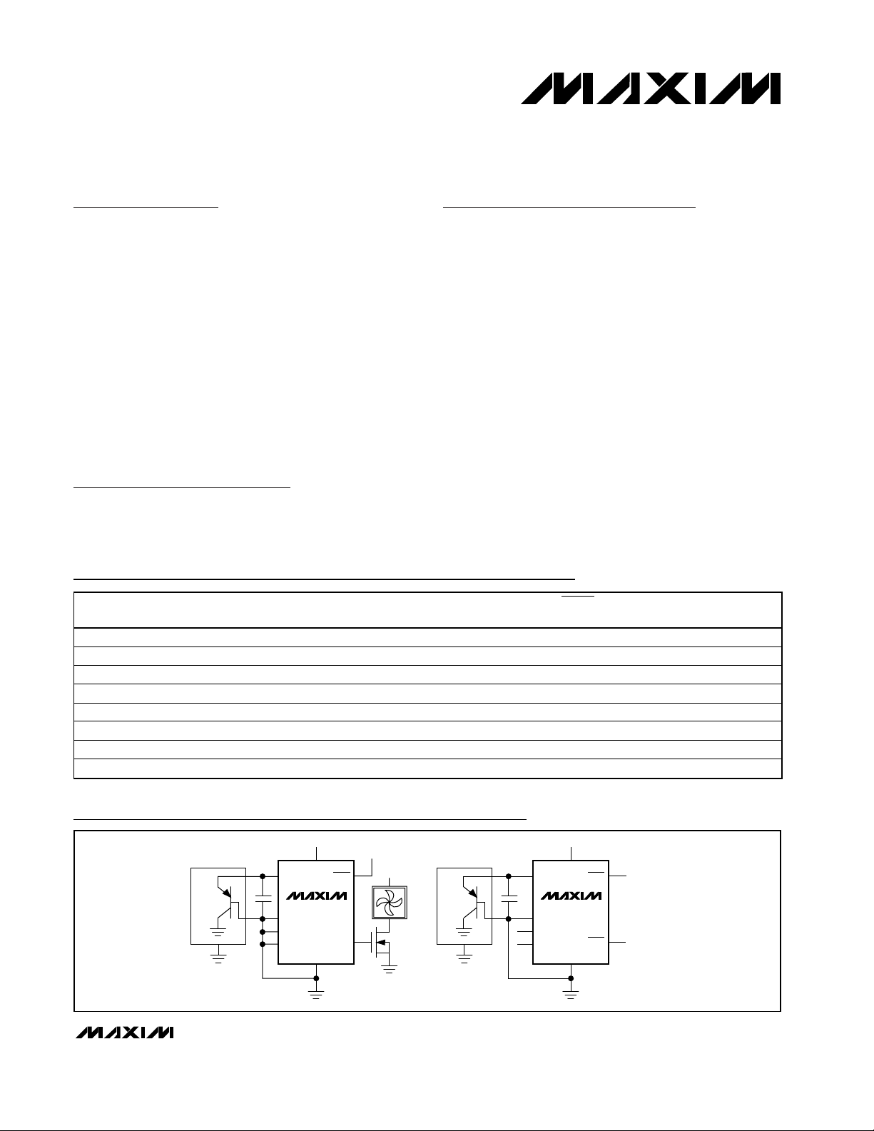
Typical Operating Circuits
19-2459; Rev 2; 4/03
For pricing, delivery, and ordering information, please contact Maxim/Dallas Direct! at
1-888-629-4642, or visit Maxim’s website at www.maxim-ic.com.
Pin Configurations appear at end of data sheet.
CPU Temperature
Protection
Fan Control
Multichip Modules
FPGA Temperature
Protection
T
PART
MAX6685AU40L Push-pull, active high +40°C to +80°C +120°C 8 µMAX
MAX6685AU40H Push-pull, active high +40°C to +80°C +125°C 8 µMAX
MAX6685AU75L Push-pull, active high +75°C to +115°C +120°C 8 µMAX
MAX6685AU75H Push-pull, active high +75°C to +115°C +125°C 8 µMAX
MAX6686AU40L Open drain, active low +40°C to +80°C +120°C 8 µMAX
MAX6686AU40H Open drain, active low +40°C to +80°C +125°C 8 µMAX
MAX6686AU75L Open drain, active low +75°C to +115°C +120°C 8 µMAX
MAX6686AU75H Open drain, active low +75°C to +115°C +125°C 8 µMAX
LOW
OUTPUT
TRIP
T
LOW
RANGE (0°C)
T
TRIP
HIGH
THRESHOLD (0°C)
PIN-PACKAGE
MAX6685/MAX6686
Dual-Output Remote-Junction
Temperature Switches
2 _______________________________________________________________________________________
ABSOLUTE MAXIMUM RATINGS
ELECTRICAL CHARACTERISTICS
(VDD= 3.0V to 5.5V, TA= -40°C to +125°C, unless otherwise noted. Typical values are at VDD= 3.3V and TA= +25°C.) (Note 1)
Stresses beyond those listed under “Absolute Maximum Ratings” may cause permanent damage to the device. These are stress ratings only, and functional
operation of the device at these or any other conditions beyond those indicated in the operational sections of the specifications is not implied. Exposure to
absolute maximum rating conditions for extended periods may affect device reliability.
Voltages Referenced to GND
V
DD, TLOW
, T
HIGH
.....................................................-0.3V to +6V
DXN .......................................................................-0.3V to +0.8V
All Other Pins..............................................-0.3V to (V
DD
+ 0.3V)
Input Current .........................................................................5mA
Output Current ....................................................................20mA
Continuous Power Dissipation (T
A
= +70°C)
8-Pin µMAX (derate 4.1mW/°C above +70°C) .............330mW
Operating Temperature Range .........................-40°C to +125°C
Junction Temperature......................................................+150°C
Storage Temperature Range .............................-65°C to +165°C
Lead Temperature (soldering, 10s) .................................+300°C
Note 1: All parameters are tested at +25°C. Temperature specifications over a range of -40°C to +125°C are guaranteed by design.
Note 2: T
RJ
is the temperature of the remote-sensing diode junction.
Power-Supply Range V
Average Supply Current I
Supply Current During
Conversion
Power-On Reset Threshold POR V
POR Threshold Hysteresis 50 mV
Temperature Threshold
Accuracy
Temperature Threshold
Hysteresis
Supply Sensitivity of Temperature
Threshold
Output Voltage High V
Output Voltage Low V
Logic-Low Input Voltage V
Logic-High Input Voltage V
Input Current S1, S2 10 µA
Open-Drain Output Leakage
Current
Conversion Time 0.09 0.11 0.13 s
Sample Period 0.35 0.45 0.55 s
Current Sourcing for External
Diode
PARAMETER SYMBOL CONDITION MIN TYP MAX UNITS
DD
DD
falling edge 1.0 1.5 2.0 V
DD
VDD = 3.3V, TA = +25°C, TRJ = 0°C to +125°C
∆T
T
HYST
(Note 2)
TH
TA = 0°C to +100°C, TRJ = 0°C to +125°C 2.0
TA = +25°C, TRJ = 0°C to +125°C,
V
= 3.0V to 5.5V
DD
OHISOURCE
OLISINK
S1, S2 0.4 V
IL
S1, S2 1.8 V
IH
V
High level 80 100 120
Low level 8 10 12
= 1mA, MAX6685 T
= 1mA 0.2 V
OUT
= 5.5V, T
LOW
and T
HIGH
LOW
only
3.0 5.5 V
200 500 µA
400 800 µA
-1.5 +1.5
5.0 °C
0.6 °C/V
V
-
DD
0.2
1µA
°C
V
µA
MAX6685/MAX6686
Dual-Output Remote-Junction
Temperature Switches
_______________________________________________________________________________________ 3
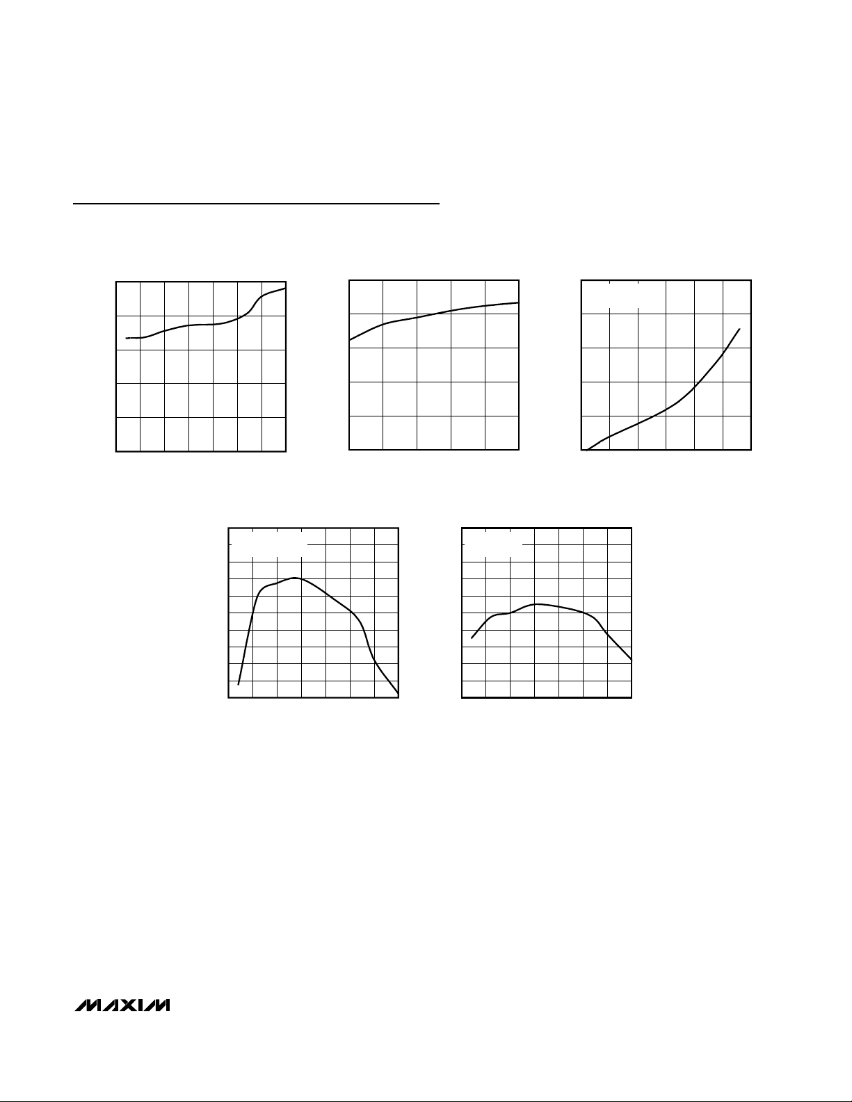
Typical Operating Characteristics
(VDD= 3.3V, CS= 2200pF, TA= +25°C, unless otherwise noted. See Typical Operating Circuits.)
AVERAGE SUPPLY CURRENT
vs. AMBIENT TEMPERATURE
200
180
160
140
120
AVERAGE SUPPLY CURRENT (µA)
100
-50 125
AMBIENT TEMPERATURE (°C)
UPPER TEMPERATURE TRIP THRESHOLD
2.0
1.6
1.2
0.8
0.4
0
-0.4
-0.8
-1.2
UPPER TRIP THRESHOLD ERROR (°C)
-1.6
-2.0
-50 125
250
MAX6685 toc01
200
150
100
AVERAGE SUPPLY CURRENT (µA)
1007550250-25
ERROR vs. AMBIENT TEMPERATURE
MAX6685U40H
TRIP = +125°C
T
HIGH
AMBIENT TEMPERATURE (°C)
AVERAGE SUPPLY CURRENT
vs. SUPPLY VOLTAGE
50
0
3.0 5.5
SUPPLY VOLTAGE (V)
5.04.54.03.5
LOWER TEMPERATURE TRIP THRESHOLD
ERROR vs. AMBIENT TEMPERATURE
2.0
MAX6685U40H
1.6
MAX6685 toc04
1007525 500-25
S1 = S2 = V
1.2
0.8
0.4
0
-0.4
-0.8
-1.2
LOWER TRIP THRESHOLD ERROR (°C)
-1.6
-2.0
-50 125
10
MAX6685 toc02
TEMPERATURE TRIP THRESHOLD ERROR (°C)
DD
AMBIENT TEMPERATURE (°C)
TEMPERATURE TRIP THRESHOLD ERROR
MAX6685U40H
S1 = S2 = GND
8
6
4
2
0
060
1007525 500-25
CAPACITANCE
vs. C
S
CS CAPACITANCE (nF)
MAX6685 toc05
MAX6685 toc03
5040302010

MAX6685/MAX6686
Detailed Description
The MAX6685/MAX6686 dual-output remote-sensing
junction temperature switches incorporate a precision
remote-junction temperature sensor and two comparators. These devices use an external P-N junction as the
temperature-sensing element (see Typical Operating
Circuits).
The MAX6685/MAX6686 provide noise immunity by
integration and oversampling of the diode voltage, but
good design practice includes routing the DXP and
DXN lines away from noise sources, such as highspeed digital lines, switching regulators, inductors, and
transformers. The DXP and DXN traces should be
paired together and surrounded by a ground plane
whenever possible.
The 5°C hysteresis keeps the outputs from “chattering”
when the measured temperature is close to the threshold
temperature. The MAX6685/MAX6686 are available with
preset upper temperature thresholds of +120°C or
+125°C. The lower temperature thresholds are pin programmable in 5°C increments (Table 1). Two tempera-
ture ranges are available for the lower trip threshold:
+40°C to +80°C and +75°C to +115°C. S1 and S2 pins
must be set to the desired trip temperature before power
is applied to the VDDpin. If this is done after the power is
turned on, the lower trip threshold remains set to the
point where S1 and S2 were when power was applied.
Applications Information
Remote-Diode Selection
The MAX6685/MAX6686 are optimized to measure the
die temperature of CPUs and other ICs that have on-chip
temperature-sensing diodes. These on-chip diodes are
substrate PNPs with their collectors grounded. Connect
the base of the PNP to DXN and the emitter to DXP. When
using a discrete, diode-connected NPN or PNP as a
sensing diode, use a good-quality small-signal device.
Examples are listed in Table 2. Tight specifications for forward current gain indicate the manufacturer has good
process controls and that the devices have consistent
V
be
characteristics. Always use a transistor for the sens-
ing junction; diodes do not work.
Dual-Output Remote-Junction
Temperature Switches
4 _______________________________________________________________________________________
Pin Description
PIN
MAX6685 MAX6686
11VDDPower-Supply Input. Bypass to GND with a 0.1µF capacitor.
2 2 GND Ground
3 3 DXP
4 4 DXN
55T
6—T
—6T
77S1
88S2
NAME FUNCTION
This pin connects to the positive (anode) terminal of the external P-N sense junction. It sources
current into the external junction. A 2200pF capacitor should be connected across DXP and DXN.
This pin connects to the negative (cathode) terminal of the external P-N sense junction. It sinks
current from the external junction. A 2200pF capacitor should be connected across DXP and
DXN. DXN must be connected to the GND pin with the shortest possible connection.
Open-Drain, Active-Low Output. T
programmed upper temperature threshold, either +120°C or +125°C. Connect a pullup resistor
HIGH
(typically 10kΩ) between T
CMOS Push-Pull, Active-High Output. T
LOW
programmed lower temperature threshold.
Open-Drain, Active-Low Output. T
programmed lower temperature threshold. Connect a pullup resistor (typically 10kΩ) between
LOW
T
and a positive supply up to 5.5V.
LOW
Threshold Select Input. Used in conjunction with S2 to set the lower threshold for T
It can be connected to V
Threshold Select Input. Used in conjunction with S1 to set the lower threshold for T
It can be connected to V
goes low when the temperature exceeds the factory-
HIGH
and a positive supply up to 5.5V.
HIGH
goes HIGH when the temperature exceeds the pin-
LOW
goes LOW when the temperature exceeds the pin-
LOW
, GND, or left floating.
DD
, GND, or left floating.
DD
(Table 1).
LOW
(Table 1).
LOW

Noise-Filtering Capacitors
A quality ceramic capacitor must be connected across
the DXP/DXN inputs to maintain temperature threshold
accuracy by filtering out noise. The capacitor should be
located physically close to the DXP/DXN pins and
should typically have a value of 2200pF. Larger capacitor values can cause temperature measurement errors.
A 50% variation from the recommended capacitor
value can cause up to ±1°C error.
MAX6685/MAX6686
Dual-Output Remote-Junction
Temperature Switches
_______________________________________________________________________________________ 5
Figure 1. MAX6685 Functional Diagram
Figure 2. MAX6686 Functional Diagram
MAX6685AUA40L
MAX6685AUA40H
MAX6686AUA40L
MAX6686AUA40H
MAX6685AUA75L
MAX6685AUA75H
MAX6686AUA75L
MAX6686AUA75H
S1 S2
LOWER TEMPERATURE
TRIP THRESHOLD (°C)
LOWER TEMPERATURE
TRIP THRESHOLD (°C)
GND GND +40 +75
GND FLOAT +45 +80
GND V
DD
+50 +85
FLOAT GND +55 +90
FLOAT FLOAT +60 +95
FLOAT V
DD
+65 +100
V
DD
GND +70 +105
V
DD
FLOAT +75 +110
V
DD
V
DD
+80 +115
Table 1. Lower Temperature Trip Threshold Selection
Table 2. Sensor Transistor Manufacturers
Note: Discrete transistors must be diode connected (base
shorted to collector).
Central Semiconductor (USA) CMPT3904
ON Semiconductor (USA) 2N3904, 2N3906
Rohm Semiconductor (Japan) SST3904
Samsung (Korea) KST3904-TF
Siemens (Germany) SMBT3904
MANUFACTURER MODEL NO.
V
DD
T
HIGH
+120°C OR +125°C
DXP
DXN
S1
S2
REMOTE
TEMPERATURE
CONVERTER
T
LOW
+40°C TO +115°C
GND
DIGITAL
DRIVER
MAX6685
T
HIGH
N
T
LOW
DXP
DXN
S1
S2
T
HIGH
+120°C OR +125°C
REMOTE
TEMPERATURE
CONVERTER
T
LOW
+40°C TO +115°C
V
DD
GND
MAX6686
T
HIGH
N
T
LOW
N

MAX6685/MAX6686
Dual-Output Remote-Junction
Temperature Switches
6 _______________________________________________________________________________________
Pin Configurations
Chip Information
TRANSISTOR COUNT: 7765
PROCESS: BiCMOS
TOP VIEW
V
DXP
DXN
1
DD
2
MAX6685
3
4
µMAX
87S2
6
5
1
V
DD
S1GND
T
LOW
T
HIGH
DXP
DXN
2
MAX6686
3
4
µMAX
87S2
6
5
S1GND
T
LOW
T
HIGH

MAX6685/MAX6686
Dual-Output Remote-Junction
Temperature Switches
Maxim cannot assume responsibility for use of any circuitry other than circuitry entirely embodied in a Maxim product. No circuit patent licenses are
implied. Maxim reserves the right to change the circuitry and specifications without notice at any time.
Maxim Integrated Products, 120 San Gabriel Drive, Sunnyvale, CA 94086 408-737-7600 _____________________ 7
© 2003 Maxim Integrated Products Printed USA is a registered trademark of Maxim Integrated Products.
Package Information
(The package drawing(s) in this data sheet may not reflect the most current specifications. For the latest package outline information,
go to www.maxim-ic.com/packages
.)
b
E H
A1
4X S
BOTTOM VIEW
A
c
L
SIDE VIEW
8
1
DIM
A
A1
A2
b
c
D
e
E
H
L
α
S
INCHES
MIN
-
0.002
0.030
0.010
0.005
0.116
0.0256 BSC
0.116
0.188
0.016
0∞
0.0207 BSC
0.037
0.007
0.198
0.026
MAX
0.043
0.006
0.014
0.120
0.120
6∞
MILLIMETERS
0.05 0.15
0.25 0.36
0.13 0.18
2.95 3.05
2.95 3.05
4.78
0.41
MIN
- 1.10
0.65 BSC
0.5250 BSC
MAX
0.950.75
5.03
0.66
8LUMAXD.EPS
6∞0∞
α
8
ÿ 0.50±0.1
0.6±0.1
0.6±0.1
1
D
TOP VIEW
A2
e
FRONT VIEW
PROPRIETARY INFORMATION
TITLE:
PACKAGE OUTLINE, 8L uMAX/uSOP
REV.DOCUMENT CONTROL NO.APPROVAL
21-0036
1
J
1
 Loading...