Maxim MAX667EPA, MAX667ESA, MAX667C-D, MAX667CPA, MAX667CSA Datasheet
...
19-3894; Rev 3; 10/94
+5V/Programmable Low-Dropout
_______________General Description
The MAX667 low-dropout, positive, linear voltage regulator supplies up to 250mA of output current. With no
load, it has a typical quiescent current of 20µA. At
200mA of output current, the input/output voltage differential is typically 150mV. Other features include a lowvoltage detector to indicate power failure, as well as
early-warning and low-dropout detectors to indicate an
imminent loss of output voltage regulation. A shutdown
control disables the output and puts the circuit into a
low quiescent-current mode.
The MAX667 employs Dual Mode™ operation. One
mode uses internally trimmed feedback resistors to produce +5V. In the other mode, the output may be varied
from +1.3V to +16V by connecting two external resistors.
The MAX667 is a pin-compatible upgrade to the
MAX666 in most applications where the input voltages
are above +3.5V. Choose the MAX667 when high output currents and/or low dropout voltages are desired,
as well as for improved performance at higher
temperatures.
________________________Applications
Battery-Powered Devices
Pagers and Radio Control Receivers
Portable Instruments
Solar-Powered Instruments
Voltage Regulator
____________________________Features
♦ 350mV Max Dropout at 200mA
♦ 250mA Output Current
♦ Normal Mode: 20µA Typ Quiescent Current
Shutdown Mode: 0.2µA Typ Quiescent Current
♦ Low-Battery Detector
♦ Fixed +5V (Min Component Count) or
Adjustable Output
♦ +3.5V to +16.5V Input
♦ Dropout Detector Output
♦ 10µF Output Capacitor
______________Ordering Information
PART TEMP. RANGE PIN-PACKAGE
MAX667CPA 0°C to +70°C 8 Plastic DIP
MAX667CSA 0°C to +70°C 8 SO
MAX667C/D 0°C to +70°C
MAX667EPA -40°C to +85°C 8 Plastic DIP
MAX667ESA -40°C to +85°C 8 SO
MAX667MJA -55°C to +125°C 8 CERDIP
* Contact factory for dice specifications.
Dice
*
MAX667
MAX667
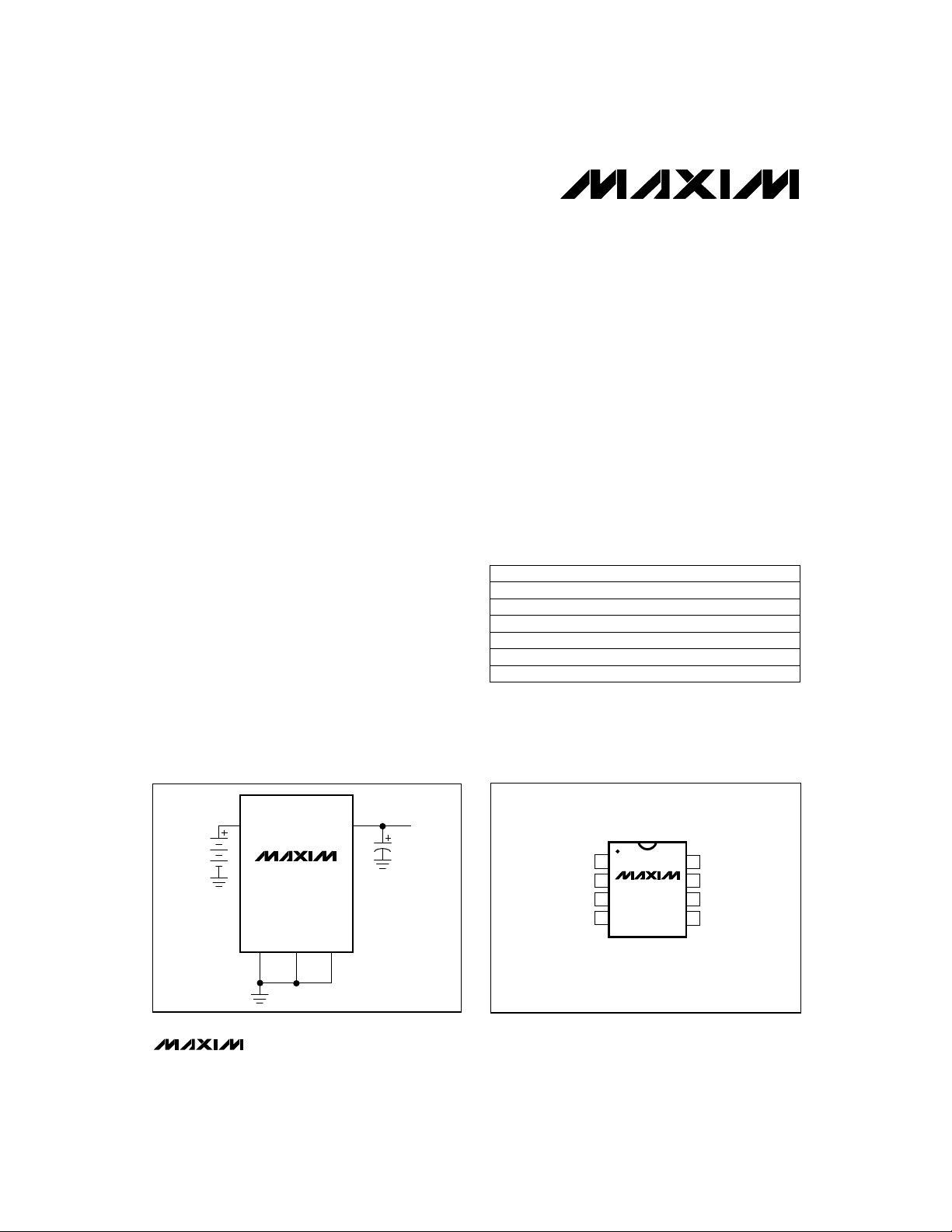
__________Typical Operating Circuit
IN
+6.3V
BATTERY
MAX667
TM
Dual Mode is a trademark of Maxim Integrated Products.
________________________________________________________________
OUT
GND SHDNSET
C1
10µF
+5V OUT
__________________Pin Configuration
TOP VIEW
1
DD
2
OUT
LBI
GND
MAX667
3
4
DIP/SO
Maxim Integrated Products
Call toll free 1-800-998-8800 for free samples or literature.
8
IN
7
LBO
6
SET
5
SHDN
1

+5V/Programmable Low-Dropout
Voltage Regulator
ABSOLUTE MAXIMUM RATINGS
Input Supply Voltage ...........................................................+18V
Output Short Circuited to Ground.........................................1sec
LBO Output Sink Current....................................................50mA
LBO Output Voltage...............................................GND to V
SHDN Input Voltage....................................-0.3V to (VIN+ 0.3V)
Input Voltages LBI, SET................................-0.3V to (V
Continuous Power Dissipation
MAX667
Plastic DIP (derate 9.09mW/°C above +70°C) ............727mW
Stresses beyond those listed under “Absolute Maximum Ratings” may cause permanent damage to the device. These are stress ratings only, and functional
operation of the device at these or any other conditions beyond those indicated in the operational sections of the specifications is not implied. Exposure to
absolute maximum rating conditions for extended periods may affect device reliability.
IN
OUT
- 1.0V)
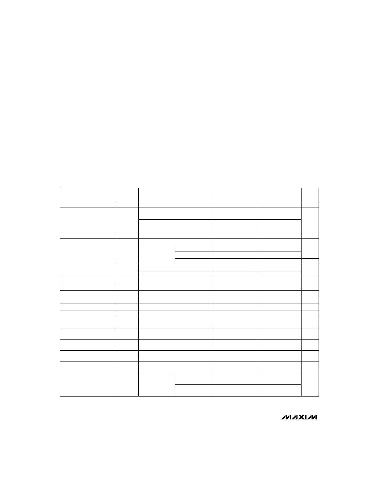
ELECTRICAL CHARACTERISTICS
(GND = 0V, VIN= +9V, V
PARAMETER
Input Voltage
Output Voltage
Maximum Output Current I
Quiescent Current I
Dropout Voltage (Note1)
Load Regulation
Line Regulation
SET Reference Voltage V
SET Input Leakage Current I
Output Leakage Current
Short-Circuit Current
Low-Battery Detector
Reference Voltage
Low-Battery Detector
Input Leakage Current
Low-Battery Detector
Output Voltage
SHDN Threshold
SHDN Leakage Current
Dropout Detector Output
Voltage
Note 1: Dropout Voltage is V
Note 2: Short-Circuit Current is pulse tested to maintain junction temperature. Short-circuit duration is limited by package dissipation.
= +5V, C1 = 10µF, unless otherwise noted.)
OUT
SYMBOL
V
IN
V
OUT
OUT
Q
SET
SET
I
OUT
I
OUT
V
LBI
I
LBI
V
LBO
V
SHDN
I
SHDN
V
DD
IN-VOUT
V
TA= -40°C to +85°C
V
TA= -55°C to +125°C
VIN= 6V, 4.5V < V
V
V
V
I
I
I
VIN= 6V to 10V, I
V
(Note 2)
VIN= 9V, V
V
V
V
V
RDD= 100kΩ,
I
when V
CONDITIONS
= 0V, VIN= 6V, I
SET
= 0V, VIN= 6V, I
SET
LBI
OUT
I
I
I
OUT
= 2V, I
IN
VIN= 7V
VIN= 4.5V
OUT
OUT
OUT
= 2V
SHDN
= 0V,
SHDN
= 0V
SET
= 100µA
OUT
= 200mA
OUT
= 10mA to 200mA
OUT
= 1.5V nA
SET
= 2V
SHDN
= 1.5V nA
LBI
IH
IL
= 0V to V
SHDN
= 0V,
SET
= 0V,
SHDN
= 10mA
OUT
falls to 0.1V below its value at VIN= V
OUT
SO (derate 5.88mW/°C above +70°C).........................471mW
CERDIP (derate 8.00mW/°C above +70°C).................640mW
Operating Temperature Ranges
MAX667C_A........................................................0°C to +70°C
MAX667E_A.....................................................-40°C to +85°C
MAX667MJA..................................................-55°C to +125°C
Storage Temperature Range.............................-65°C to +160°C
Lead Temperature (soldering, 10sec).............................+300°C
TA= +25°C
MIN TYP MAX
TA= T
MIN TYP MAX
MIN
to T
3.5 16.5
= 10mA,
OUT
OUT
< 5.5V
= 10mA,
250 250
5 4.8 5.2
5 4.75 5.25
0.2 1
= 0µA
= 100µA
= 200mA
20 25 35
20 30
515 20
560 75
150 250
50 100 250
= 10mA
510
1.225
1.20 1.25
0.01 ±10 ±1000V
0.1 1
400
1.225 1.195 1.255
0.01 ±10 ±1000V
LBO
= 10mA
1.5
0.25 0.4
1.5
0.3 0.3V
0.01 ±10 ±1000
3.5
+ 2V.
OUT
MAX
2
50
350
15
450
0.25
UNITS
V
V
mA
µA
mA
mV
mV
mV
V
µA
mA
V
V
V
nA
V
2 _______________________________________________________________________________________

+5V/Programmable Low-Dropout
Voltage Regulator
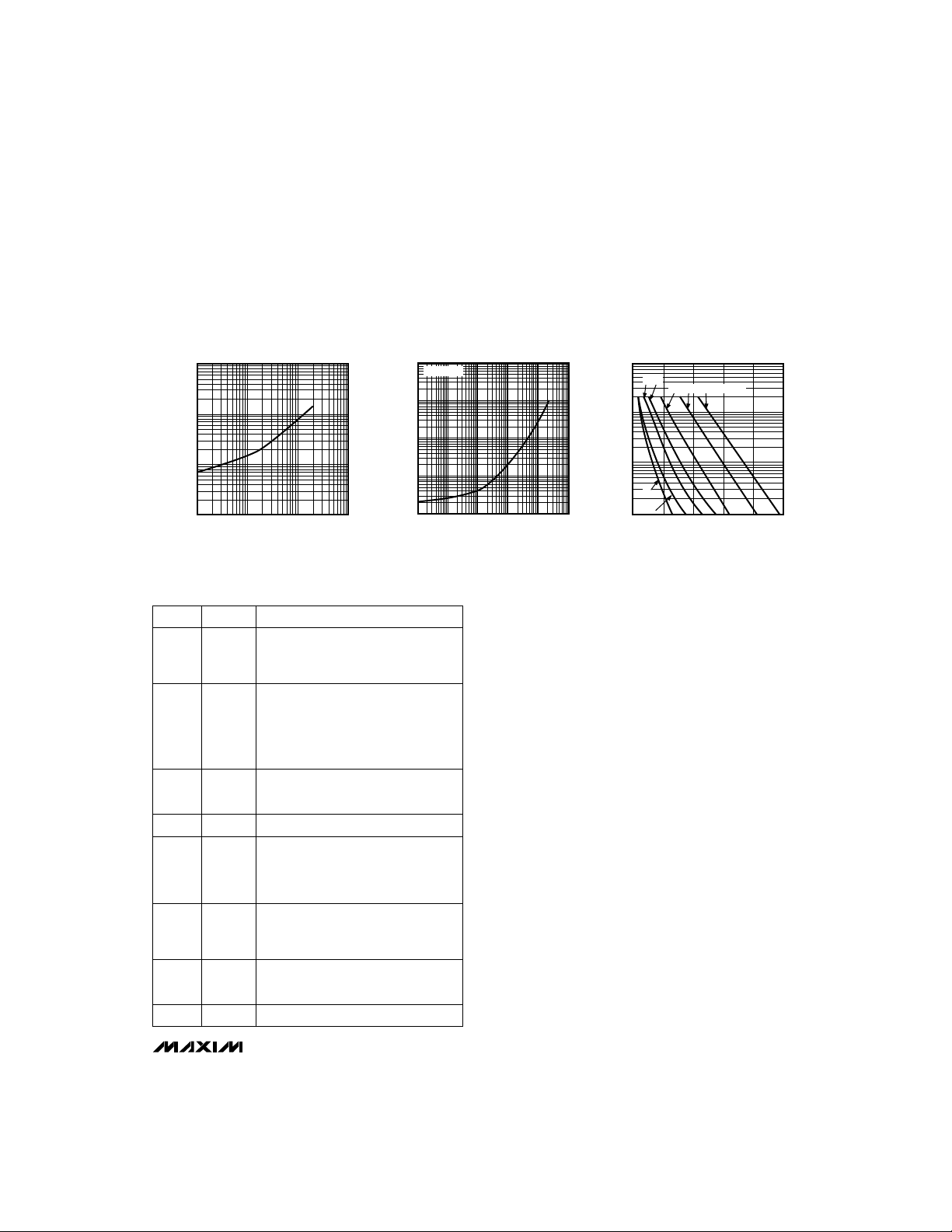
__________________________________________Typical Operating Characteristics
(TA= +25°C, unless otherwise noted.)
DROPOUT VOLTAGE
1000
100
10
DROPOUT VOLTAGE (mV)
1
vs. LOAD CURRENT
1 10 100 1000
LOAD CURRENT (mA)
MAX667-Fg TOC 1
QUIESCENT CURRENT
100,000
10,000
1000
QUIESCENT CURRENT (µA)
100
10
vs. LOAD CURRENT
VIN = +6V
0.01 0.1 1 10 100 1000
LOAD CURRENT (mA)
1000
MAX667-Fg TOC 2
100
10
DD OUTPUT CURRENT (µA)
1
DD OUTPUT CURRENT
vs. INPUT-OUTPUT DIFFERENCE
5 10
20 50 100mA LOAD
1
2
0 50 150 250
100 200
INPUT-OUTPUT DIFFERENCE (mV)
MAX667-Fg TOC 3
_____________________Pin Description _______________Detailed Description
Figure 1 shows a micropower bandgap reference, an
PIN
FUNCTIONNAME
Dropout Detector Output—the collec-
DD1
OUT2
LBI3
SHDN5
SET6
LBO7
tor of a PNP pass transistor. Normally
an open circuit, it sources current as
dropout is reached.
Regulated Output Voltage. OUT falls
to 0V when SHDN is above 1.5V. SET
determines output voltage when SET
is above 50mV; otherwise, it is 5V.
OUT must be connected to an output
filter capacitor.
Low-Battery Detector. A CMOS input
to an internal 1.255V comparator
whose output is the LBO pin.
GroundGND4
Shutdown Input. Connect to GND for
normal operation (output active). Pull
above 1.5V to disable OUT, LBO, and
DD and to reduce quiescent current to
less than 1µA.
(Output) Voltage Set, CMOS Input.
Connect to GND for 5V output. For
other voltages, connect external resistive divider from OUT.
Low-Battery Output. An open-drain Nchannel transistor that sinks current to
GND when LBI is less than 1.22V.
Positive Input Voltage (unregulated)IN8
error amplifier, a PNP pass transistor, and two comparators as the main elements of the MAX667. One
comparator, C1, selects the fixed 5V or adjustable
operation with an external voltage divider. The other
comparator, C2, is a low-battery detector.
The bandgap reference, which is trimmed to 1.22V,
connects internally to one input of the error amplifier,
A1. The feedback signal from the regulator output supplies the other input of A1 from either an on-chip voltage divider or two external resistors. When SET is
grounded, the internal divider provides the error amplifier feedback signal for a fixed 5V output. When SET is
more than 50mV above ground, the error amplifier’s
input switches directly to SET while an external resistor
divider from OUT determines the output voltage.
A second comparator, C2, compares the LBI input to
the internal reference voltage. LBO is an open-drain
FET connected to GND. The low-battery threshold can
also be set with a voltage divider at LBI. In addition, the
MAX667 has a shutdown input (SHDN) that disables
the load and the device while reducing quiescent current when it is pulled high.
+5V Output
Figure 2 shows the connection for a fixed 5V output.
The SET input is grounded, and no external resistors
are required. Figure 3 shows adjustable output operation. R1 and R2 set the output voltage. SHDN should be
grounded if not used.
MAX667
_______________________________________________________________________________________ 3
 Loading...