

19-3894; Rev 3; 10/94
+5V/Programmable Low-Dropout
_______________General Description
The MAX667 low-dropout, positive, linear voltage regulator supplies up to 250mA of output current. With no
load, it has a typical quiescent current of 20µA. At
200mA of output current, the input/output voltage differential is typically 150mV. Other features include a lowvoltage detector to indicate power failure, as well as
early-warning and low-dropout detectors to indicate an
imminent loss of output voltage regulation. A shutdown
control disables the output and puts the circuit into a
low quiescent-current mode.
The MAX667 employs Dual Mode™ operation. One
mode uses internally trimmed feedback resistors to produce +5V. In the other mode, the output may be varied
from +1.3V to +16V by connecting two external resistors.
The MAX667 is a pin-compatible upgrade to the
MAX666 in most applications where the input voltages
are above +3.5V. Choose the MAX667 when high output currents and/or low dropout voltages are desired,
as well as for improved performance at higher
temperatures.
________________________Applications
Battery-Powered Devices
Pagers and Radio Control Receivers
Portable Instruments
Solar-Powered Instruments
Voltage Regulator
____________________________Features
♦ 350mV Max Dropout at 200mA
♦ 250mA Output Current
♦ Normal Mode: 20µA Typ Quiescent Current
Shutdown Mode: 0.2µA Typ Quiescent Current
♦ Low-Battery Detector
♦ Fixed +5V (Min Component Count) or
Adjustable Output
♦ +3.5V to +16.5V Input
♦ Dropout Detector Output
♦ 10µF Output Capacitor
______________Ordering Information
PART TEMP. RANGE PIN-PACKAGE
MAX667CPA 0°C to +70°C 8 Plastic DIP
MAX667CSA 0°C to +70°C 8 SO
MAX667C/D 0°C to +70°C
MAX667EPA -40°C to +85°C 8 Plastic DIP
MAX667ESA -40°C to +85°C 8 SO
MAX667MJA -55°C to +125°C 8 CERDIP
* Contact factory for dice specifications.
Dice
*
MAX667
MAX667
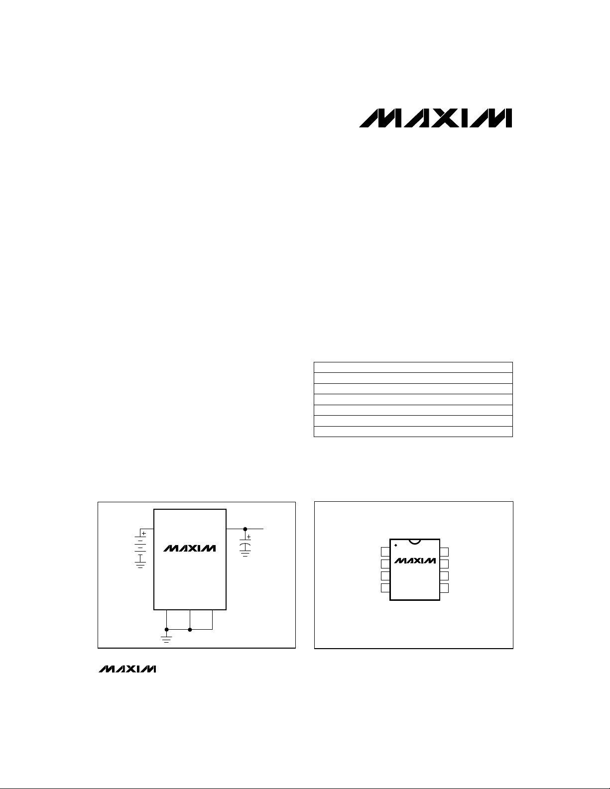
__________Typical Operating Circuit
IN
+6.3V
BATTERY
MAX667
TM
Dual Mode is a trademark of Maxim Integrated Products.
________________________________________________________________
OUT
GND SHDNSET
C1
10µF
+5V OUT
__________________Pin Configuration
TOP VIEW
1
DD
2
OUT
LBI
GND
MAX667
3
4
DIP/SO
Maxim Integrated Products
Call toll free 1-800-998-8800 for free samples or literature.
8
IN
7
LBO
6
SET
5
SHDN
1
+5V/Programmable Low-Dropout
Voltage Regulator
ABSOLUTE MAXIMUM RATINGS
Input Supply Voltage ...........................................................+18V
Output Short Circuited to Ground.........................................1sec
LBO Output Sink Current....................................................50mA
LBO Output Voltage...............................................GND to V
SHDN Input Voltage....................................-0.3V to (VIN+ 0.3V)
Input Voltages LBI, SET................................-0.3V to (V
Continuous Power Dissipation
MAX667
Plastic DIP (derate 9.09mW/°C above +70°C) ............727mW
Stresses beyond those listed under “Absolute Maximum Ratings” may cause permanent damage to the device. These are stress ratings only, and functional
operation of the device at these or any other conditions beyond those indicated in the operational sections of the specifications is not implied. Exposure to
absolute maximum rating conditions for extended periods may affect device reliability.
IN
OUT
- 1.0V)
ELECTRICAL CHARACTERISTICS
(GND = 0V, VIN= +9V, V
PARAMETER
Input Voltage
Output Voltage
Maximum Output Current I
Quiescent Current I
Dropout Voltage (Note1)
Load Regulation
Line Regulation
SET Reference Voltage V
SET Input Leakage Current I
Output Leakage Current
Short-Circuit Current
Low-Battery Detector
Reference Voltage
Low-Battery Detector
Input Leakage Current
Low-Battery Detector
Output Voltage
SHDN Threshold
SHDN Leakage Current
Dropout Detector Output
Voltage
Note 1: Dropout Voltage is V
Note 2: Short-Circuit Current is pulse tested to maintain junction temperature. Short-circuit duration is limited by package dissipation.
= +5V, C1 = 10µF, unless otherwise noted.)
OUT
SYMBOL
V
IN
V
OUT
OUT
Q
SET
SET
I
OUT
I
OUT
V
LBI
I
LBI
V
LBO
V
SHDN
I
SHDN
V
DD
IN-VOUT
V
TA= -40°C to +85°C
V
TA= -55°C to +125°C
VIN= 6V, 4.5V < V
V
V
V
I
I
I
VIN= 6V to 10V, I
V
(Note 2)
VIN= 9V, V
V
V
V
V
RDD= 100kΩ,
I
when V
CONDITIONS
= 0V, VIN= 6V, I
SET
= 0V, VIN= 6V, I
SET
LBI
OUT
I
I
I
OUT
= 2V, I
IN
VIN= 7V
VIN= 4.5V
OUT
OUT
OUT
= 2V
SHDN
= 0V,
SHDN
= 0V
SET
= 100µA
OUT
= 200mA
OUT
= 10mA to 200mA
OUT
= 1.5V nA
SET
= 2V
SHDN
= 1.5V nA
LBI
IH
IL
= 0V to V
SHDN
= 0V,
SET
= 0V,
SHDN
= 10mA
OUT
falls to 0.1V below its value at VIN= V
OUT
SO (derate 5.88mW/°C above +70°C).........................471mW
CERDIP (derate 8.00mW/°C above +70°C).................640mW
Operating Temperature Ranges
MAX667C_A........................................................0°C to +70°C
MAX667E_A.....................................................-40°C to +85°C
MAX667MJA..................................................-55°C to +125°C
Storage Temperature Range.............................-65°C to +160°C
Lead Temperature (soldering, 10sec).............................+300°C
TA= +25°C
MIN TYP MAX
TA= T
MIN TYP MAX
MIN
to T
3.5 16.5
= 10mA,
OUT
OUT
< 5.5V
= 10mA,
250 250
5 4.8 5.2
5 4.75 5.25
0.2 1
= 0µA
= 100µA
= 200mA
20 25 35
20 30
515 20
560 75
150 250
50 100 250
= 10mA
510
1.225
1.20 1.25
0.01 ±10 ±1000V
0.1 1
400
1.225 1.195 1.255
0.01 ±10 ±1000V
LBO
= 10mA
1.5
0.25 0.4
1.5
0.3 0.3V
0.01 ±10 ±1000
3.5
+ 2V.
OUT
MAX
2
50
350
15
450
0.25
UNITS
V
V
mA
µA
mA
mV
mV
mV
V
µA
mA
V
V
V
nA
V
2 _______________________________________________________________________________________
+5V/Programmable Low-Dropout
Voltage Regulator
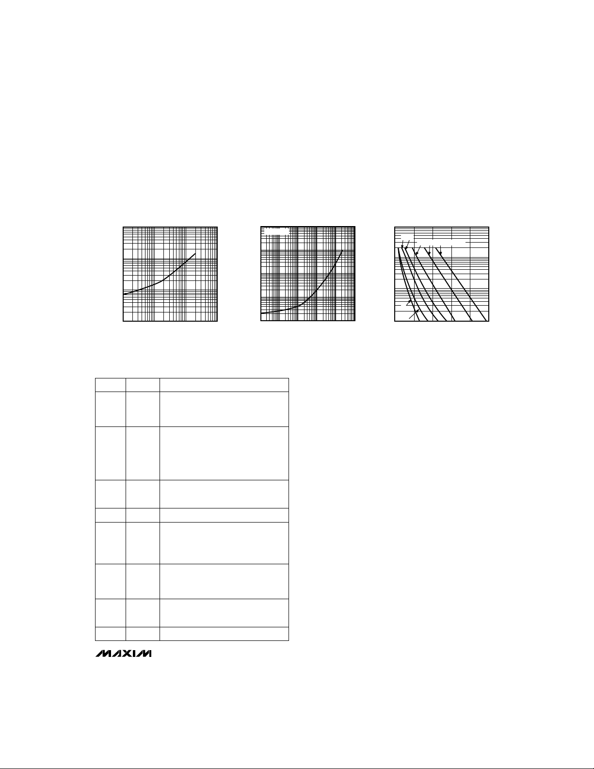
__________________________________________Typical Operating Characteristics
(TA= +25°C, unless otherwise noted.)
DROPOUT VOLTAGE
1000
100
10
DROPOUT VOLTAGE (mV)
1
vs. LOAD CURRENT
1 10 100 1000
LOAD CURRENT (mA)
MAX667-Fg TOC 1
QUIESCENT CURRENT
100,000
10,000
1000
QUIESCENT CURRENT (µA)
100
10
vs. LOAD CURRENT
VIN = +6V
0.01 0.1 1 10 100 1000
LOAD CURRENT (mA)
1000
MAX667-Fg TOC 2
100
10
DD OUTPUT CURRENT (µA)
1
DD OUTPUT CURRENT
vs. INPUT-OUTPUT DIFFERENCE
5 10
20 50 100mA LOAD
1
2
0 50 150 250
100 200
INPUT-OUTPUT DIFFERENCE (mV)
MAX667-Fg TOC 3
_____________________Pin Description _______________Detailed Description
Figure 1 shows a micropower bandgap reference, an
PIN
FUNCTIONNAME
Dropout Detector Output—the collec-
DD1
OUT2
LBI3
SHDN5
SET6
LBO7
tor of a PNP pass transistor. Normally
an open circuit, it sources current as
dropout is reached.
Regulated Output Voltage. OUT falls
to 0V when SHDN is above 1.5V. SET
determines output voltage when SET
is above 50mV; otherwise, it is 5V.
OUT must be connected to an output
filter capacitor.
Low-Battery Detector. A CMOS input
to an internal 1.255V comparator
whose output is the LBO pin.
GroundGND4
Shutdown Input. Connect to GND for
normal operation (output active). Pull
above 1.5V to disable OUT, LBO, and
DD and to reduce quiescent current to
less than 1µA.
(Output) Voltage Set, CMOS Input.
Connect to GND for 5V output. For
other voltages, connect external resistive divider from OUT.
Low-Battery Output. An open-drain Nchannel transistor that sinks current to
GND when LBI is less than 1.22V.
Positive Input Voltage (unregulated)IN8
error amplifier, a PNP pass transistor, and two comparators as the main elements of the MAX667. One
comparator, C1, selects the fixed 5V or adjustable
operation with an external voltage divider. The other
comparator, C2, is a low-battery detector.
The bandgap reference, which is trimmed to 1.22V,
connects internally to one input of the error amplifier,
A1. The feedback signal from the regulator output supplies the other input of A1 from either an on-chip voltage divider or two external resistors. When SET is
grounded, the internal divider provides the error amplifier feedback signal for a fixed 5V output. When SET is
more than 50mV above ground, the error amplifier’s
input switches directly to SET while an external resistor
divider from OUT determines the output voltage.
A second comparator, C2, compares the LBI input to
the internal reference voltage. LBO is an open-drain
FET connected to GND. The low-battery threshold can
also be set with a voltage divider at LBI. In addition, the
MAX667 has a shutdown input (SHDN) that disables
the load and the device while reducing quiescent current when it is pulled high.
+5V Output
Figure 2 shows the connection for a fixed 5V output.
The SET input is grounded, and no external resistors
are required. Figure 3 shows adjustable output operation. R1 and R2 set the output voltage. SHDN should be
grounded if not used.
MAX667
_______________________________________________________________________________________ 3

+5V/Programmable Low-Dropout
Voltage Regulator
MAX667
Figure 1. MAX667 Block Diagram
8
IN
IN
SHDN
LBO
LBI
GND
MAX667
A1
C2 C1
1.255V REF
OUT
2
C1
10µF
+5V OUT
250mA
OUT
DD
SET
+50mV
MAX667
8
IN
LBO
7
N
R3
MAX667
OUT
VREF
2
V
OUT
C1
10µF
R2
LBI
3
GND SHDNSET
645
Figure 2. Fixed +5V Regulator
R4
GNDSHDN
54
Figure 3. Adjustable Output and Low-Battery Detector
4 _______________________________________________________________________________________
SET
6
R1

+5V/Programmable Low-Dropout
If SET is connected to a resistive voltage divider (Figure
3), the output voltage is set by the equation:
V
where V
To simplify resistor selection:
Since the input bias current at SET has a maximum
value of 10nA, relatively large values can be used for
R1 and R2 with no loss of accuracy. 1MΩ is a typical
value for R1. The V
This allows the output to be preset without trim pots,
using only fixed resistors in most cases. However,
when resistor values greater than 1MΩ are used, pay
special attention to printed circuit board leakage that
can introduce error at the SET input.
SHDN puts the device into standby mode to conserve
power. When this pin is held low, the IC operates normally. If it is driven above 1.5V, the chip shuts down.
Quiescent current of the MAX667 is then reduced to
less than 1µA, and OUT turns off.
Note that the voltage for SHDN must never be more
than 0.3V higher than VIN.
The MAX667 contains circuitry for low-battery detection. If the voltage at LBI falls below the regulator’s
internal reference (1.22V), LBO, an open-drain output,
sinks current to GND. The threshold can be set to any
level above the reference voltage by connecting a
resistive divider to LBI based on the equation:
where V
detector, and R3 and R4 are the LBI input divider
resistors.
Since LBI input current is no more than 10nA, high values for R3 and R4 minimize loading. If V
5.5V low-battery threshold can be set using 8.2MΩ for
R3 and 2.4MΩ for R4. When resistor values greater
than 1MΩ are used, pay special attention to PC board
leakage that can introduce error at the LBI input.
When the voltage at LBI is below the internal threshold,
LBO sinks current to GND. A pull-up resistor of 10kΩ or
more connected to OUT can be used with this pin when
driving CMOS circuits. Any pull-up resistor connected
to LBO should not be returned to a voltage source
greater than V
the MAX667 is in SHDN mode, the LBO output is off.
OUT
= 1.22V
SET
R2 = R1 x (V
R3 = R4 x (V
is the desired threshold of the low-battery
BATT
OUT
Output-Voltage Selection
= V
x (R1 + R2) / R1,
SET
/ V
SET
- 1)
OUT
tolerance is less than ±25mV.
SET
Shutdown (Standby) Mode
Low-Battery Function
/ V
LBI
- 1)
OUT
is 5V, a
BATT
. When LBI is above the threshold or
Voltage Regulator
The minimum input-output differential, or dropout voltage, determines the regulator’s lowest usable input
voltage. In battery-operated systems, this determines
the useful end-of-life battery voltage. The MAX667 features very low dropout voltage (see
Characteristics
detector output, DD, that changes as the dropout voltage approaches its limit. DD is an open collector of a
PNP transistor. The dropout voltage and the dropout
detector both depend on the output current and temperature. When the input voltage is more than 300mV
above the output voltage, the dropout detector will not
conduct. As the differential decreases below 300mV,
the DD source current increases abruptly. This current
signals a warning that regulation is about to be lost.
Connecting a resistor (typically 100kΩ) from DD to
ground develops a voltage that can be monitored by
analog circuits or changed to digital levels by a comparator. LBI may be used for this purpose.
). In addition, the MAX667 has a dropout
__________Applications Information
As with all PNP output regulators, an output capacitor
(C1, Figure 2) is required to maintain stability. 10µF is
recommended. To ensure stability, the output-capacitor
ESR must be sufficiently high. Figure 4 shows the minimum required output-capacitor ESR for a given temperature. Alternatively, a resistor may be added in series
with the output capacitor (Figure 5); the sum of the out-
5
4
3
2
MINIMUM ESR (Ω)
1
0
-60 -40 -20 0 20 40 60 80 100 120
Figure 4. Minimum Required Output-Capacitor ESR vs.
Temperature
TEMPERATURE (˚C)
Dropout Detector
Electrical
Output Capacitor
MAX667-Fg 4
MAX667
MAX667
_______________________________________________________________________________________ 5

+5V/Programmable Low-Dropout
Voltage Regulator
82
OUT
+5V OUTIN
8
OUT
2
C1
10µF
+5V OUTIN
R
10µF
MAX667
MAX667
SHDNSET GND
645
Figure 5. Alternative Stability Scheme Using Resistor R
8
OUT
2
C1
10µF
+5V OUTIN
MAX667
1
DD
GND SHDNSET
645
R1
47k
C2
0.1µF
Figure 6. Quiescent-Current Reduction Below Dropout
put-capacitor ESR and this series resistance should, at
minimum, meet the requirements shown in Figure 4.
An upper limit to the output-capacitor ESR is important
only if step changes to the load are anticipated. Higher
ESR results in higher-amplitude output-voltage transients when the output current is varied. A Sanyo
OS-CON capacitor, whose ESR is nearly flat over temperature (and is low to begin with), in series with the
appropriate resistor ensures the best load-transient
performance. A less expensive alternative is to use a
tantalum capacitor in series with the resistor.
MAX667
5
SHDN
41
SET
DDGND
R3
1M
6
R2
1M
R1
332k
Figure 7. Connection for Minimum Quiescent Current Near
Dropout
10
V
SHDN = 0V
8
6
4
QUIESCENT CURRENT (mA)
2
0
0123456
INPUT VOLTAGE (V)
MAX667-Fg 8
Figure 8. Quiescent Current Below Dropout for Circuit of
Figure 2
In most cases, inexpensive aluminum-electrolytic
capacitors work well with the MAX667 over their entire
temperature range, having sufficient ESR to ensure stability without the need for a series resistor. The ESR of
aluminium electrolytics rises, often dramatically, as
temperature decreases. For surface-mount applications, certain tantalum capacitors have sufficient ESR;
an example is the TAJB106K016 chip capacitor made
by AVX (phone: (803) 448-9411, fax: (803) 448-1943).
Battery Drain
The MAX667 uses a PNP output transistor. When the
input voltage falls below the desired output voltage, the
6 _______________________________________________________________________________________

800
600
(µA)
400
GND
I
200
0
12 4 6
CIRCUIT OF
FIGURE 7
CIRCUIT OF
FIGURE 6
35
VIN (V)
+5V/Programmable Low-Dropout
+5V/Programmable Low-Dropout
Voltage Regulator
Voltage Regulator
400
= +50˚C
T
MAX667-Fg 9
LOAD CURRENT (mA)
A
300
200
100
SO PACKAGE
DISSIPATION LIMIT
0
015
GUARANTEED 250mA
DIP PACKAGE
DISSIPATION LIMIT
5
V
IN-VOUT
10
(V)
MAX667-Fg 10
MAX667
MAX667
Figure 9. Quiescent Current Below Dropout with Connections
of Figures 6 and 7
PNP transistor is turned on fully as regulation is lost.
Even with a load current of a few microamperes, the
base current will be driven above 5mA. Figure 8 shows
how this base current may be significant.
Consequently, a mostly discharged battery can be further discharged at end-of-life.
Figure 6 shows how this condition can be modified by
connecting DD to SHDN with a 47kΩ resistor, R1, paralleled with a 0.1µF capacitor to GND. This modification reduces the no-load quiescent current to
approximately 160µA when dropout is reached (Figure
9), but increases the dropout voltage by about 0.1V.
The output voltage drops to approximately 3V once DD
begins to activate SHDN, but it does not fall to zero
because SHDN is only partially activated.
A second alternate connection (Figure 7) further
reduces quiescent current near the dropout voltage,
compared to the circuit in Figure 6. The output must be
set with external resistors (R1, R2), so DD lowers the
output voltage as the input voltage falls by sourcing
current into SET via R3. Quiescent current remains low
for inputs down to 3.5V, and peaks before falling to 0
at low input voltages. Although the current peak is
higher than with the connection in Figure 6, this may
be more useful because the quiescent current peaks
at an input voltage well below the useful range of most
batteries (Figure 9). Also, as IN falls below 5V, OUT
tracks IN minus the dropout voltage. This connection
still allows separate use of the SHDN input.
Power Dissipation
The MAX667 can regulate currents as high as 250mA
and withstand input-output differential voltages as high
_______________________________________________________________________________________ 7
Figure 10. MAX667 Load Current vs. Input-Output Differential
Voltage
+10V
INPUT
+2V/div
+6V
+5V OUTPUT
+0.2V/div
1ms/div
Figure 11. Output Response to +4V/100µs Input Step
as 15.2V, but not simultaneously. The maximum power
dissipation is dependent on the package and the temperature (see
Absolute Maximum Ratings
). Figure 10
shows the maximum output current at various inputoutput differential voltages for the plastic DIP and SO
packages. The MAX667 can withstand short-circuit
loads up to 1 second.
Operation from AC Sources
The MAX667 is a micropower CMOS regulator intended principally for battery operation. When operating
from AC sources, consider power-supply ripple rejection. The MAX667’s error amplifier produces very low
gain bandwidth, and the input power-supply rejection

+5V/Programmable Low-Dropout
Voltage Regulator
___________________Chip Topography
+5V OUTPUT
0.1V/div
MAX667
100mA
OUTPUT
CURRENT
10mA
200µs/div
Figure 12. Output Response to 10mA/100mA Load Step with
10µF Output Capacitor (1.5Ω ESR)
ratio (PSRR) is therefore not specified. Since the output
must be connected to a 10µF or larger filter capacitor,
the capacitor characteristics dominate the PSRR. Large
values of input and output capacitors reduce the ripple.
In addition, both DD and LBI/LBO can trigger on the
lowest DC component of the ripple, particularly at high
load currents. In the case of the low-battery detector,
the ripple can be effectively filtered out by placing a
capacitor to ground in parallel with the LBI input pin.
The high resistance values that can be used for the
voltage divider allow relatively small capacitance values to form an effective lowpass filter at 120Hz. When
power is first applied, however, this filter tends to hold
LBO low longer than normal.
The low operating current and gain-bandwidth product
of the internal reference and amplifier result in limited
rejection of fast-step input changes. Negative-going
steps, which occur in under 100µs, may turn off the output for several milliseconds. An input filter (nominally
10µF) is recommended if input changes greater than
1V and faster than 100µs (other than turn-on or turn-off)
are anticipated. Figure 12 shows the output response
to a 10mA/100mA instantaneous load step. The relationship between output-capacitor ESR and load-transient response is explained in the
section.
Transient Considerations
Output Capacitor
OUT
DD
LBI
GND
IN
0.107"
(2.71mm)
LBO
SET
SHDN
0.070"
(1.78mm)
TRANSISTOR COUNT: 65
SUBSTRATE MUST BE LEFT UNCONNECTED
Maxim cannot assume responsibility for use of any circuitry other than circuitry entirely embodied in a Maxim product. No circuit patent licenses are
implied. Maxim reserves the right to change the circuitry and specifications without notice at any time.
8
___________________Maxim Integrated Products, 120 San Gabriel Drive, Sunnyvale, CA 94086 (408) 737-7600
© 1994 Maxim Integrated Products Printed USA is a registered trademark of Maxim Integrated Products.
 Loading...