

Page 1
General Description
The MAX6678 monitors its own temperature and the
temperatures of two external diode-connected transistors, which typically reside on the die of a CPU or other
integrated circuit. The device reports temperature values
in digital form using a 2-wire serial interface. The
MAX6678 provides a programmable alarm output to generate interrupts, throttle signals, or overtemperature shutdown signals.
The 2-wire serial interface accepts standard System
Management Bus (SMBus)™write byte, read byte, send
byte, and receive byte commands to read the temperature data and program the alarm thresholds. The temperature data controls a PWM output signal to adjust
the speed of a cooling fan, thereby minimizing noise
when the system is running cool, but providing maximum cooling when power dissipation increases.
Five GPIO pins provide additional flexibility. The GPIO
power-up states are set by connecting the GPIO preset
inputs to ground or VCC.
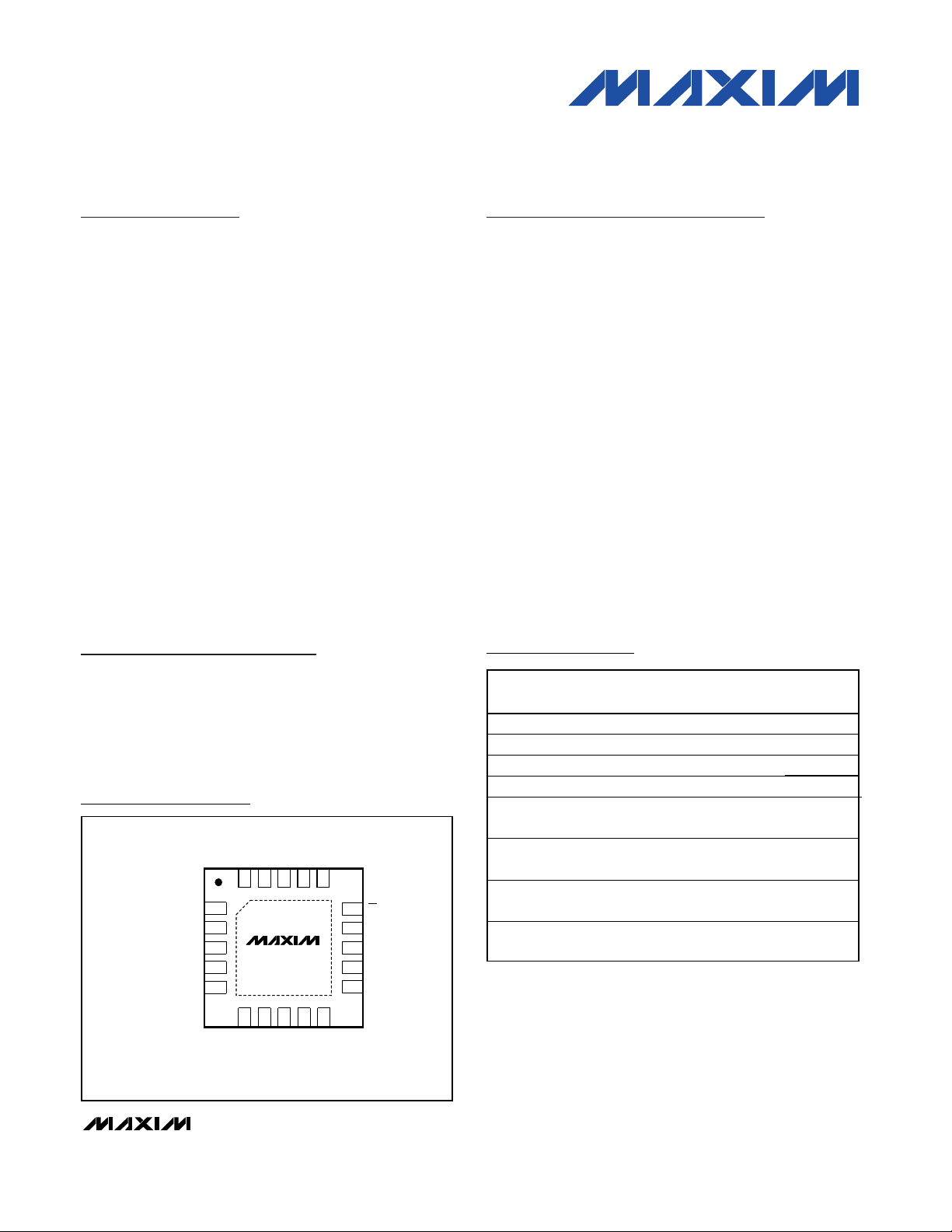
The MAX6678 is available in a 20-pin QSOP package
and a 5mm x 5mm thin QFN package. It operates from
3.0V to 5.5V and consumes just 500µA of supply current.
Applications
Desktop Computers
Notebook Computers
Workstations
Servers
Networking Equipment
Features
♦ Two Thermal-Diode Inputs
♦ Local Temperature Sensor
♦ Five GPIO Input/Outputs
♦ Two PWM Outputs for Fan Drive (Open Drain; May
Be Pulled Up to +5V)
♦ Programmable Fan-Control Characteristics
♦ Automatic Fan Spin-Up Ensures Fan Start
♦ Controlled Rate of Change Ensures Unobtrusive
Fan-Speed Adjustments
♦ 1°C Remote Temperature Accuracy (+60°C to
+145°C)
♦ Temperature Monitoring Begins at POR for Fail-
Safe System Protection
♦ OT Output for Throttling or Shutdown
♦ Four Versions Available, Each with a Different
Address
♦ 5mm x 5mm TQFN Package
MAX6678
2-Channel Temperature Monitor with Dual Automatic
PWM Fan-Speed Controller and Five GPIOs
________________________________________________________________ Maxim Integrated Products 1
Pin Configurations
Ordering Information
19-3306; Rev 0; 5/04
For pricing, delivery, and ordering information, please contact Maxim/Dallas Direct! at
1-888-629-4642, or visit Maxim’s website at www.maxim-ic.com.
*EP = Exposed paddle.
SMBus is a trademark of Intel Corp.
Pin Configurations continued at end of data sheet.
Typical Operating Circuit appears at end of data sheet.
CC
PRESET3
PWMOUT2
V
MAX6678
GND
DXP2
PWMOUT116GPIO0
10
PRESET2
PRESET1
OT
15
GPIO1
14
GPIO2
13
12
GPIO3
11
PRESET0
TOP VIEW
SMBDATA
SMBCLK
GPIO4
PRESET4
20 19 18 17
1
2
3
4
*CONNECT EXPOSED
5DXP1
PADDLE TO GND
6789
DXN
5mm x 5mm THIN QFN
PART TEMP RANGE
MAX6678AEP90 -40°C to +125°C 20 QSOP 1001000
MAX6678AEP92 -40°C to +125°C 20 QSOP 1001001
MAX6678AEP94 -40°C to +125°C 20 QSOP 1001010
MAX6678AEP96 -40°C to +125°C 20 QSOP 1001011
MAX6678ATP90 -40°C to +125°C
MAX6678ATP92 -40°C to +125°C
MAX6678ATP94 -40°C to +125°C
MAX6678ATP96 -40°C to +125°C
PINPACKAGE
20 Thin
QFN-EP*
20 Thin
QFN-EP*
20 Thin
QFN-EP*
20 Thin
QFN-EP*
SMBus
ADDRESS
1001000
1001001
1001010
1001011
Page 2

MAX6678
2-Channel Temperature Monitor with Dual Automatic
PWM Fan-Speed Controller and Five GPIOs
2 _______________________________________________________________________________________
ABSOLUTE MAXIMUM RATINGS
ELECTRICAL CHARACTERISTICS
(VCC= +3.0V to +5.5V, TA= -40°C to +125°C, unless otherwise noted. Typical values are at VCC= +3.3V, TA= +25°C.)
Stresses beyond those listed under “Absolute Maximum Ratings” may cause permanent damage to the device. These are stress ratings only, and functional
operation of the device at these or any other conditions beyond those indicated in the operational sections of the specifications is not implied. Exposure to
absolute maximum rating conditions for extended periods may affect device reliability.
VCCto GND..............................................................-0.3V to +6V
OT, SMBDATA, SMBCLK, PWMOUT_,
GPIO_ to GND ......................................................-0.3V to +6V
DXP_ to GND ..........................................-0.3V to + (V
CC
+ 0.3V)
DXN to GND ..........................................................-0.3V to +0.8V
PRESET_ to GND ....................................-0.3V to + (V
CC
+ 0.3V)
SMBDATA, OT, PWMOUT_ Current....................-1mA to +50mA
DXN Current .......................................................................±1mA
ESD Protection (all pins, Human Body Model) ..................2000V
Continuous Power Dissipation (T
A
= +70°C)
20-Pin QSOP (derate 9.1mW/°C above +70°C).......... 727mW
20-Pin TQFN (derate 34.5mW/°C above +70°C) .......2759mW
Operating Temperature Range .........................-40°C to +125°C
Junction Temperature......................................................+150°C
Storage Temperature Range ............................-65°C to +150°C
Lead Temperature (soldering, 10s) .................................+300°C
Operating Supply Voltage Range V
Operating Current I
External Temperature Error,
V
CC
Internal Temperature Error VCC = +3.3V
Temperature Resolution
Conversion Time 200 250 300 ms
PWM Frequency Tolerance (Note 1) -20 +20 %
Remote-Diode Sourcing Current
DXN Source Voltage 0.7 V
DIGITAL INPUTS AND OUTPUTS
Output Low Voltage (Sink Current)
(OT, GPIO_, SMBDATA, PWMOUT_)
Output High Leakage Current
(OT, GPIO_, SMBDATA, PWMOUT_)
Logic-Low Input Voltage (SMBDATA,
SMBCLK, PRESET_, GPIO_)
Logic-High Input Voltage (SMBDATA,
SMBCLK, PRESET_, GPIO_)
Input Leakage Current 1µA
Input Capacitance C
SMBus TIMING
Serial Clock Frequency f
PARAMETER SYMBOL CONDITIONS MIN TYP MAX UNITS
CC
Interface inactive, ADC active 0.5 1 mA
S
+25°C ≤ TR ≤ +125°C,
T
= 60°C
A
= 3.3V
V
OL
I
OH
V
IL
V
IH
IN
SCLK
VCC = 3.3V
High level 80 100 120
Low level 8 10 12
I
= 6mA 0.4 V
OUT
VCC = 3V to 3.6V 0.8
VCC = 3.6V to 5.5V 0.8
VCC = 3V to 3.6V 2.1
VCC = 3.6V to 5.5V 2.1
0°C ≤ T
+25°C ≤ T
0°C ≤ T
0°C ≤ T
+25°C ≤ TR ≤ +100°C ±2.5
0°C ≤ T
≤ +145°C,
R
≤ +100°C
A
≤ +145°C,
R
≤ +125°C
A
≤ +125°C ±4
A
+3.0 +5.5 V
±1
±3
±4
1°C
8 Bits
1µA
5pF
100 kHz
°C
°C
µA
V
V
Page 3
MAX6678
2-Channel Temperature Monitor with Dual Automatic
PWM Fan-Speed Controller and Five GPIOs
_______________________________________________________________________________________ 3
ELECTRICAL CHARACTERISTICS (continued)
(VCC= +3.0V to +5.5V, TA= -40°C to +125°C, unless otherwise noted. Typical values are at VCC= +3.3V, TA= +25°C.)
Note 1: Deviation from programmed value in Table 6.
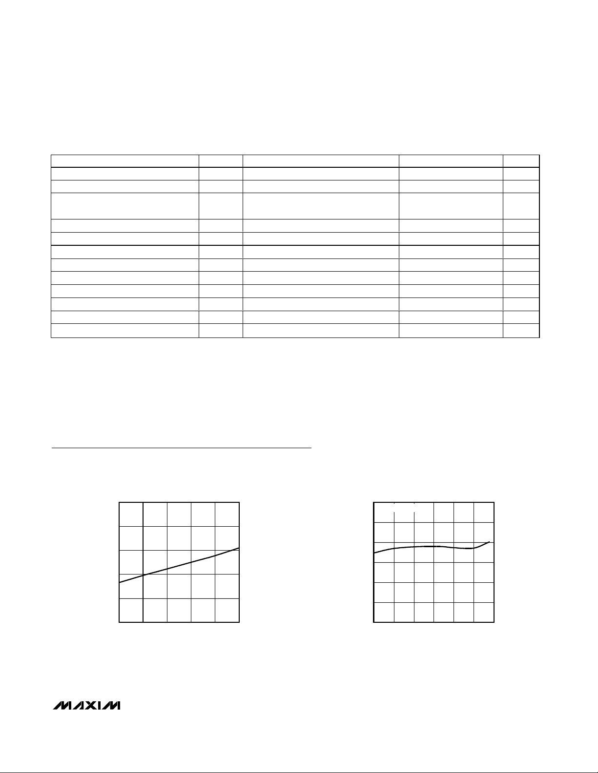
Typical Operating Characteristics
(TA = +25°C, unless otherwise noted.)
400
440
520
480
560
600
3.0 4.03.5 4.5 5.0 5.5
OPERATING SUPPLY CURRENT
vs. SUPPLY VOLTAGE
MAX6678 toc02
SUPPLY VOLTAGE (V)
SUPPLY CURRENT (µA)
-4
-2
-3
0
-1
1
2
050
7525100
125 150
REMOTE TEMPERATURE ERROR
vs. REMOTE-DIODE TEMPERATURE
MAX6678 toc03
TEMPERATURE (°C)
TEMPERATURE ERROR (
°
C)
FAIRCHILD 2N3906
Clock Low Period t
Clock High Period t
Bus Free Time Between Stop and
Start Conditions
SMBus Start Condition Setup Time t
Start Condition Hold Time t
Stop Condition Setup Time t
Data Setup Time t
Data Hold Time t
SMBus Fall Time t
SMBus Rise Time t
SMBus Timeout t
Startup Time After POR t
PARAMETER SYMBOL CONDITIONS MIN TYP MAX UNITS
LOW
HIGH
t
BUF
SU:STA
HD:STO
SU:STO
SU:DAT
HD:DAT
TIMEOUT
POR
10% to 10% 4 µs
90% to 90% 4.7 µs
4.7 µs
90% of SMBCLK to 90% of SMBDATA 4.7 µs
10% of SMBDATA to 10% of SMBCLK 4 µs
90% of SMBCLK to 10% of SMBDATA 4 µs
10% of SMBDATA to 10% of SMBCLK 250 ns
10% of SMBCLK to 10% of SMBDATA 300 ns
F
R
29 37 55 ms
300 ns
1000 ns
500 ms
Page 4
MAX6678
2-Channel Temperature Monitor with Dual Automatic
PWM Fan-Speed Controller and Five GPIOs
4 _______________________________________________________________________________________
Typical Operating Characteristics (continued)
(TA = +25°C, unless otherwise noted.)
-3
-1
-2
1
0
2
3
05025 75 100 125
LOCAL TEMPERATURE ERROR
vs. DIE TEMPERATURE
MAX6678 toc04
TEMPERATURE (°C)
TEMPERATURE ERROR (
°
C)
-1.5
0
-0.5
-1.0
1.0
0.5
1.5
2.0
0.01 10.1 10 100 1000
REMOTE TEMPERATURE ERROR
vs. POWER-SUPPLY NOISE FREQUENCY
MAX6678 toc05
FREQUENCY (kHz)
TEMPERATURE ERROR (
°
C)
VIN = 250mV
P-P
SQUARE WAVE APPLIED
TO V
CC
WITH NO BYPASS CAPACITOR
-2.5
-1.0
-1.5
-2.0
0
-0.5
0.5
1.0
0.01 10.1 10 100 1000
LOCAL TEMPERATURE ERROR
vs. POWER-SUPPLY NOISE FREQUENCY
MAX6678 toc06
FREQUENCY (kHz)
TEMPERATURE ERROR (
°
C)
VIN = 250mV
P-P
SQUARE WAVE APPLIED
TO V
CC
WITH NO BYPASS CAPACITOR
0
1.4
1.2
1.0
0.8
0.6
0.4
0.2
1.8
1.6
2.0
0.01 10.1 10 100 1000
REMOTE TEMPERATURE ERROR
vs. COMMON-MODE NOISE FREQUENCY
MAX6678 toc07
FREQUENCY (kHz)
TEMPERATURE ERROR (
°
C)
VIN = AC-COUPLED TO DXP AND DXN
V
IN
= 100mV
P-P
SQUARE WAVE
0
0.7
0.6
0.5
0.4
0.3
0.2
0.1
0.9
0.8
1.0
0.01 10.1 10 100 1000
REMOTE TEMPERATURE ERROR
vs. DIFFERENTIAL NOISE FREQUENCY
MAX6678 toc08
FREQUENCY (kHz)
TEMPERATURE ERROR (
°
C)
VIN = AC-COUPLED TO DXP
V
IN
= 100mV
P-P
SQUARE WAVE
-6
-3
-5
-4
-1
-2
1
0
2
0.1 1 10 100
TEMPERATURE ERROR
vs. DXP-DXN CAPACITANCE
MAX6678 toc09
DXP-DXN CAPACITANCE (nF)
TEMPERATURE ERROR (
°
C)
TA = +25°C
30
31
33
32
34
35
-40 10 35-15 60 11085
PWMOUT FREQUENCY
vs. DIE TEMPERATURE
MAX6678 toc10
TEMPERATURE (°C)
PWMOUT FREQUENCY (Hz)
30
31
33
32
34
35
3.0 4.03.5 4.5 5.0 5.5
PWMOUT FREQUENCY
vs. SUPPLY VOLTAGE
MAX6678 toc11
SUPPLY VOLTAGE (V)
PWMOUT FREQUENCY (Hz)
0
100
300
200
400
500
0101552025303540
GPIO OUTPUT VOLTAGE
vs. GPIO SINK CURRENT
MAX6678 toc12
GPIO SINK CURRENT (mA)
GPIO OUTPUT VOLTAGE (mV)
Page 5
Detailed Description
The MAX6678 temperature sensor and fan controller
accurately measures the temperature of either two
remote pn junctions or one remote pn junction and its
own die. The device reports temperature values in digital form using a 2-wire serial interface. The remote pn
junction is typically the emitter-base junction of a common-collector pnp on a CPU, FPGA, or ASIC. The
MAX6678 operates from supply voltages of 3.0V to
5.5V and consumes 500µA (typ) of supply current. The
temperature data controls a PWM output signal to
adjust the speed of a cooling fan. The device also features an overtemperature alarm output to generate
interrupts, throttle signals, or shutdown signals.
Five GPIO input/outputs provide additional flexibility.
The GPIO power-up states are set by connecting the
GPIO preset inputs to ground or V
CC
.
MAX6678
2-Channel Temperature Monitor with Dual Automatic
PWM Fan-Speed Controller and Five GPIOs
_______________________________________________________________________________________ 5
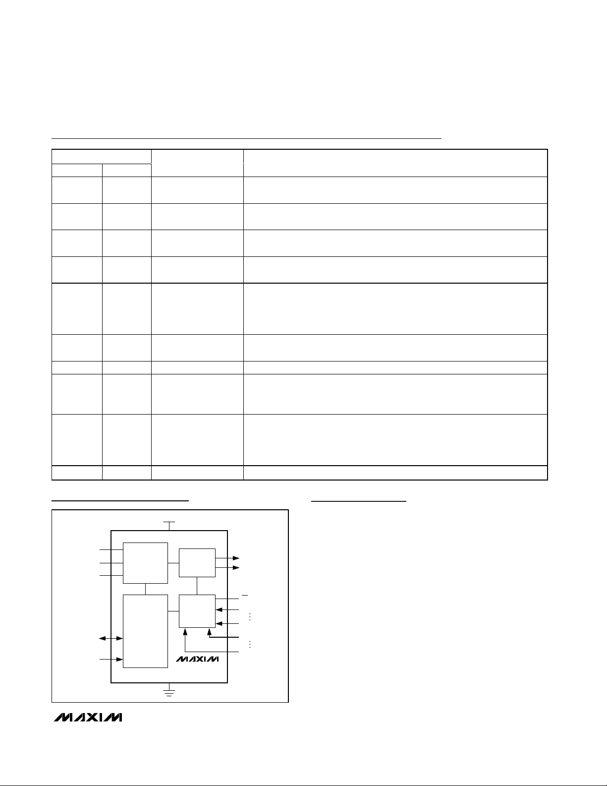
Pin Description
Block Diagram
PIN
THIN QFN QSOP
13 SMBDATA
24 SMBCLK
3, 12, 13,
14, 16
4, 9, 10,
11, 20
5, 7 7, 9 DXP1, DXP2
68 DXN
810 GND Ground. Connect to a clean ground reference.
15 17 OT
17, 19 1, 19
18 20 V
5, 14, 15,
16, 18
2, 6, 11,
12, 13
NAME DESCRIPTION
SMBus Serial-Data Input/Output, Open Drain. Can be pulled up to 5.5V,
regardless of V
SMBus Serial-Clock Input. Can be pulled up to 5.5V, regardless of V
circuit when V
GPIO0–GPIO4
PRESET0–PRESET4 GPIO Preset Inputs. Connect to GND or V
PWMOUT1,
PWMOUT2
CC
Active-Low, Open-Drain GPIO Pins. Can be pulled up to 5.5V, regardless of
. Open circuit when VCC = 0.
V
CC
Combined Current Source and A/D Positive Input for Remote Diode. Connect to
anode of remote-diode-connected temperature-sensing transistor. Do not leave
floating; connect to DXN if no remote diode is used. Place a 2200pF capacitor
between DXP_ and DXN for noise filtering.
Combined Remote-Diode Cathode Input. Connect cathode of the remote-diodeconnected transistor to DXN.
Active-Low, Open-Drain Over-Temperature Output. Typically used for system
shutdown or clock throttling. Can be pulled up to 5.5V regardless of V
circuit when V
Open-Drain Output to Power Transistor Driving Fan. Connect to the gate of a
MOSFET or base of a transistor. PWMOUT_ requires a pullup resistor. The
pullup resistor can be connected to a supply voltage as high as 5.5V,
regardless of the MAX6678’s supply voltage.
Power-Supply Input. 3.3V nominal. Bypass VCC to GND with 0.1µF capacitor.
. Open circuit when VCC = 0.
CC
= 0.
CC
= 0.
CC
. Open
CC
to set POR value of GPIO0–GPIO4.
CC
. Open
CC
DXP1
DXN
DXP2
SMBDATA
SMBCLK
V
CC
TEMPERATURE
PROCESSING
BLOCK
PWM
GENERATOR
BLOCK
PWMOUT1
PWMOUT2
OT
GPIO0
GPIO4
PRESET0
PRESET4
SMBus
INTERFACE
AND
REGISTERS
LOGIC
MAX6678
GND
Page 6
MAX6678
SMBus Digital Interface
From a software perspective, the MAX6678 appears as a
set of byte-wide registers. This device uses a standard
SMBus 2-wire/I2C-compatible serial interface to access
the internal registers. The MAX6678 has four different
slave addresses available; therefore, a maximum of four
MAX6678 devices can share the same bus.
The MAX6678 employs four standard SMBus protocols:
write byte, read byte, send byte, and receive byte
(Figures 1, 2, and 3). The shorter receive byte protocol
allows quicker transfers, provided that the correct data
register was previously selected by a read byte instruction. Use caution with the shorter protocols in multimaster
systems, since a second master could overwrite the
command byte without informing the first master.
Temperature data can be read from registers 00h and
01h. The temperature data format for these registers is
8 bits, with the LSB representing 1°C (Table 1) and the
MSB representing +128°C. The MSB is transmitted first.
All values below 0°C clip to 00h.
Table 2 details the register address and function, whether
they can be read or written to, and the power-on reset
(POR) state. See Tables 2–6 for all other register functions
and the Register Descriptions section.
Temperature Reading
The MAX6678 contains two external temperature measurement inputs to measure the die temperature of CPUs
or other ICs having on-chip temperature-sensing diodes,
or discrete diode-connected transistors as shown in the
Typical Operating Circuits. For best accuracy, the discrete diode-connected transistor should be a small-signal
device with its collector and base connected together.
The on-chip ADC converts the sensed temperature and
outputs the temperature data in the format shown in Table
1. Temperature channel 2 can be used to measure either
a remote thermal diode or the internal temperature of the
MAX6678. Bit D1 of register 02h (Table 2) selects local or
remote sensing for temperature channel 2 (1 = local). The
temperature measurement resolution is 1°C for both local
and remote temperatures. The temperature accuracy is
within ±1°C for remote temperature measurements from
+60°C to +100°C.
2-Channel Temperature Monitor with Dual Automatic
PWM Fan-Speed Controller and Five GPIOs
6 _______________________________________________________________________________________
Write Byte Format
Read Byte Format
Send Byte Format
Receive Byte Format
Slave address: equivalent to chip-select line of
a 3-wire interface
Command byte: selects which
register you are writing to
Data byte: data goes into the register
set by the command byte (to set
thresholds, configuration masks, and
sampling rate)
Slave address: equivalent
to chip-select line
Command byte: selects
which register you are
reading from
Slave address: repeated
due to change in dataflow direction
Data byte: reads from
the register set by the
command byte
Command byte: sends command with no data, usually
used for one-shot command
Data byte: reads data from
the register commanded
by the last read byte or
write byte transmission;
also used for SMBus alert
response return address
S = Start condition Shaded = Slave transmission
P = Stop condition /// = Not acknowledged
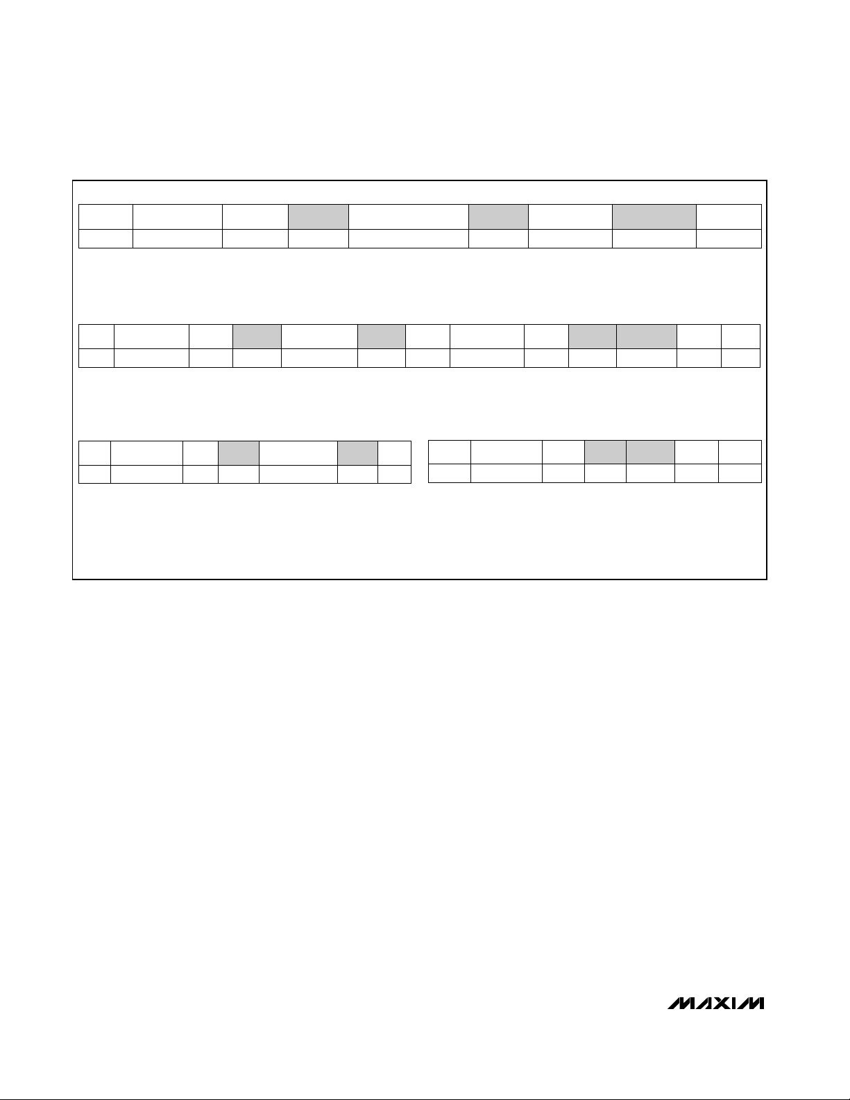
Figure 1. SMBus Protocols
S ADDRESS RD ACK DATA /// P
— 7 bits — — 8 bits — —
WRS ACK COMMAND ACK P
— — — 8 bits — —
ADDRESS
7 bits
P
1
ACK
—
DATA
8 bits
ACK
—
COMMAND
8 bits
ACK
—
WR
—
ADDRESS
7 bits
S
—
S ADDRESS WR ACK COMMAND ACK S ADDRESS
7 bits——8 bits——7 bits—
RD—ACK—DATA
8 bits
///
—
P
—
Page 7

The DXN input is biased at 0.60V above ground by an
internal diode to set up the analog-to-digital inputs for a
differential measurement. The worst case DXP-DXN differential input voltage range is from 0.25V to 0.95V.
Excess resistance in series with the remote diode causes
about +0.5°C error per ohm. Likewise, a 200µV offset
voltage forced on DXP-DXN causes about 1°C error.
High-frequency EMI is best filtered at DXP and DXN with
an external 2200pF capacitor. This value can be
increased to about 3300pF (max), including cable capacitance. Capacitance higher than 3300pF introduces
errors due to the rise time of the switched current source.
MAX6678
2-Channel Temperature Monitor with Dual Automatic
PWM Fan-Speed Controller and Five GPIOs
_______________________________________________________________________________________ 7
Figure 2. SMBus Write Timing Diagram
Figure 3. SMBus Read Timing Diagram
Table 1. Temperature Data Byte Format
AB CDEFG
t
t
HIGH
LOW
SMBCLK
SMBDATA
t
SU:STAtHD:STA
A = START CONDITION
B = MSB OF ADDRESS CLOCKED INTO SLAVE
C = LSB OF ADDRESS CLOCKED INTO SLAVE
D = R/W BIT CLOCKED INTO SLAVE
AB CDEFG HIJ
t
LOWtHIGH
SMBCLK
SMBDATA
t
t
HD:STA
SU:STA
A = START CONDITION
B = MSB OF ADDRESS CLOCKED INTO SLAVE
C = LSB OF ADDRESS CLOCKED INTO SLAVE
D = R/W BIT CLOCKED INTO SLAVE
E = SLAVE PULLS SMBDATA LINE LOW
t
SU:DAT
E = SLAVE PULLS SMBDATA LINE LOW
F = ACKNOWLEDGE BIT CLOCKED INTO MASTER
G = MSB OF DATA CLOCKED INTO SLAVE
H = LSB OF DATA CLOCKED INTO SLAVE
t
SU:DAT
F = ACKNOWLEDGE BIT CLOCKED INTO MASTER
G = MSB OF DATA CLOCKED INTO MASTER
H = LSB OF DATA CLOCKED INTO MASTER
I = MASTER PULLS DATA LINE LOW
t
HD:DAT
HIJ
I = MASTER PULLS DATA LINE LOW
J = ACKNOWLEDGE CLOCKED INTO SLAVE
K = ACKNOWLEDGE CLOCK PULSE
L = STOP CONDITION
M = NEW START CONDITION
K
J = ACKNOWLEDGE CLOCKED INTO SLAVE
K = ACKNOWLEDGE CLOCK PULSE
L = STOP CONDITION
M = NEW START CONDITION
t
SU:STOtBUF
t
SU:STO
LMK
M
L
t
BUF
TEMP (°C)
ROUNDED TEMP
(°C)
DIGITAL OUTPUT
241 +241 1111 0001
240 +240 1111 0000
126 +126 0111 1110
25 +25 0001 1001
0.50 +1 0000 0001
0.00 0 0000 0000
Diode fault (open) — 1110 1111
Diode fault (short) — 1111 1111
Page 8

MAX6678
PWM Output
1) The PWMOUT_ signals are normally used in one of
three ways to control the fan’s speed: PWMOUT_ drives the gate of a MOSFET or the base of a bipolar
transistor in series with the fan’s power supply. The
Typical Application Circuit shows the PWMOUT_ driving an n-channel MOSFET. In this case, the PWM
invert bit (D4 in register 02h) is set to 1. Figure 4
shows PWMOUT_ driving a p-channel MOSFET and
the PWM invert bit must be set to zero.
2) PWMOUT_ is converted (using an external circuit)
into a DC voltage that is proportional to duty cycle.
This duty-cycle-controlled voltage becomes the
power supply for the fan. This approach is less efficient than 1), but can result in quieter fan operation.
Figure 5 shows an example of a circuit that converts
the PWM signal to a DC voltage. Because this circuit
produces a full-scale output voltage when PWMOUT
= 0V, bit D4 in register 02h should be set to zero.
3) PWMOUT_ directly drives the logic-level PWM
speed-control input on a fan that has this type of
input. This approach requires fewer external components and combines the efficiency of 1) with the low
noise of 2). An example of PWMOUT_ driving a fan
with a speed-control input is shown in Figure 6. Bit
D4 in register 02h should be set to 1 when this configuration is used.
Whenever the fan has to start turning from a motionless
state, PWMOUT_ is forced high for 2s. After this spin-up
period, the PWMOUT_ duty cycle settles to the predetermined value. Whenever spin-up is disabled (bit 2 in
the configuration byte = 1) and the fan is off, the duty
cycle changes immediately from zero to the nominal
value, ignoring the duty-cycle rate-of-change setting.
The frequency-select register controls the frequency of
the PWM signal. When the PWM signal modulates the
power supply of the fan, a low PWM frequency (usually
33Hz) should be used to ensure the circuitry of the
brushless DC motor has enough time to operate. When
driving a fan with a PWM-to-DC circuit as in Figure 5,
the highest available frequency (35kHz) should be
used to minimize the size of the filter capacitors. When
using a fan with a PWM control input, the frequency
normally should be high as well, although some fans
have PWM inputs that accept low-frequency drive.
2-Channel Temperature Monitor with Dual Automatic
PWM Fan-Speed Controller and Five GPIOs
8 _______________________________________________________________________________________
Figure 4. Driving a P-Channel MOSFET for Top-Side PWM Fan
Drive
Figure 5. Driving a Fan with a PWM-to-DC Circuit
Figure 6. Controlling a PWM Input Fan with the MAX6678’s
PWM Output (Typically, the 35kHz PWM Frequency Is Used)
+12V
500kΩ
+3.3V
10kΩ 120kΩ
1µF
27kΩ
+3.3V
4.7kΩ
V
CC
PWMOUT
18kΩ
PWMOUT
0.01µF
1µF
5V
V
OUT
TO FAN
0.1µF
V
CC
5V
PWMOUT
10kΩ
P
Page 9

The duty cycle of the PWM can be controlled in two ways:
1) Manual PWM control by setting the duty cycle of the
fan directly through the fan target duty-cycle registers (0Bh and 0Ch).
2) Automatic PWM control by setting the duty cycle
based on temperature.
Manual PWM Duty-Cycle Control
Clearing the bits that select the temperature channels for
fan control (D5 and D4 for PWMOUT1 and D3 and D2 for
PWMOUT2) in the fan-configuration register (11h)
enables manual fan control. In this mode, the duty cycle
written to the fan target duty-cycle register directly controls the corresponding fan. The value is clipped to a
maximum of 240. Any value entered above that is
changed to 240 automatically. In this control mode, the
value in the maximum duty-cycle register is ignored and
does not affect the duty cycle used to control the fan.
Automatic PWM Duty-Cycle Control
In the automatic control mode, the duty cycle is controlled by the local or remote temperature according to
the settings in the control registers. Below the fan-start
temperature, the duty cycle is either 0% or is equal to
the fan-start duty cycle, depending on the value of bit
D3 in the configuration byte register. Above the fanstart temperature, the duty cycle increases by one duty
cycle step each time the temperature increases by one
temperature step. The target duty cycle is calculated
based on the following formula; for temperature >
FanStartTemperature:
where:
DC = DutyCycle
FSDC = FanStartDutyCycle
T = Temperature
FST = FanStartTemperature
DCSS = DutyCycleStepSize
TS = TempStep
Duty cycle is recalculated after each temperature conversion if temperature is increasing. If the temperature
begins to decrease, the duty cycle is not recalculated
until the temperature drops by 5°C from the last peak
temperature. The duty cycle remains the same until the
temperature drops 5°C from the last peak temperature or
the temperature rises above the last peak temperature.
For example, if the temperature goes up to +85°C and
starts decreasing, duty cycle is not recalculated until the
temperature reaches +80°C or the temperature rises
above +85°C. If the temperature decreases further, the
duty cycle is not updated until it reaches +75°C.
For temperature < FanStartTemperature and D2 of
configuration register = 0:
DutyCycle = 0
For temperature < FanStartTemperature and D2 of
configuration register = 1:
DutyCycle = FanStartDutyCycle
Once the temperature crosses the fan-start temperature threshold, the temperature has to drop below the
fan-start temperature threshold minus the hysteresis
before the duty cycle returns to either 0% or the fanstart duty cycle. The value of the hysteresis is set by D7
of the fan-configuration register.
The duty cycle is limited to the value in the fan maximum
duty-cycle register. If the duty-cycle value is larger than
the maximum fan duty cycle, it is set to the maximum
fan-duty cycle as in the fan maximum duty-cycle register.
The temperature step is bit D6 of the fan-configuration
register (0Dh).
Notice if temperature crosses FanStartTemperature
going up with an initial DutyCycle of zero, a spin-up of
2s applies before the duty-cycle calculation controls
the value of the fan’s duty cycle.
FanStartTemperature for a particular channel follows the
channel, not the fan. When a fan switches channels, the
start temperature also changes to that of the new channel.
If DutyCycle is an odd number, it is automatically
rounded down to the closest even number.
MAX6678
2-Channel Temperature Monitor with Dual Automatic
PWM Fan-Speed Controller and Five GPIOs
_______________________________________________________________________________________ 9
Figure 7. Automatic PWM Duty Control
DC FSDC T FST
=+ × ( ) -
DCSS
TS
DUTY CYCLE
REGISTER 02h,
BIT D3 = 1
FAN-START
DUTY CYCLE
REGISTER 02h,
BIT D3 = 0
FAN-START
TEMPERATURE
TEMP
STEP
DUTY-CYCLE
TEMPERATURE
STEP SIZE
Page 10

MAX6678
Duty-Cycle Rate-of-Change Control
To reduce the audibility of changes in fan speed, the
rate of change of the duty cycle is limited by the values
set in the duty-cycle rate-of-change register. Whenever
the target duty cycle is different from the instantaneous
duty cycle, the duty cycle increases or decreases at
the rate determined by the duty-cycle rate-of-change
byte until it reaches the target duty cycle. By setting the
rate of change to the appropriate value, the thermal
requirements of the system can be balanced against
good acoustic performance. Slower rates of change are
less noticeable to the user, while faster rates of change
can help minimize temperature variations. Remember
that the fan controller is part of a complex control system. Because several of the parameters are generally
not known, some experimentation may be necessary to
arrive at the best settings.
Power-Up Defaults
At power-up, or when the POR bit in the configuration
byte register is set, the MAX6678 has the default settings indicated in Table 2. Some of these settings are
summarized below:
• Temperature conversions are active.
• Channel 1 and channel 2 are set to report the remote
temperature channel measurements.
• Channel 1 OT limit = +110°C.
• Channel 2 OT limit = +80°C.
• Manual fan mode.
• Fan duty cycle = 0.
• PWM invert bit = 0.
• PWMOUT_ are high.
• When using an NMOS or npn transistor, the fan starts
at full speed on power-up.
OT
Output
When temperature exceeds the OT temperature threshold and OT is not masked, the OT status register indicates a fault and OT output becomes active. If OT for
the respective channel is masked off, the OT status
register continues to be set, but the OT output does not
become active.
The fault flag and the output can be cleared only by
reading the OT status register and the temperature register of that channel. If the OT status bit is cleared, OT
reasserts on the next conversion if the temperature still
exceeds the OT temperature threshold.
GPIO Inputs/Outputs and Presets
The MAX6678 contains five GPIO pins (GPIO0 through
GPIO4). When set as an output, the GPIO pin connects
to the drains of internal n-channel MOSFETs. When the
n-channel MOSFET is off, the pullup resistor (see the
Typical Operating Circuit) provides a logic-level high
output. When a GPIO pin is configured as an input, read
the state of GPIO_ from the GPIO value register (15h).
The MAX6678 powers up with GPIO0, GPIO1, and
GPIO2 high impedance and GPIO3 and GPIO4 pulled
low. After 2ms, the GPIOs go to their assigned preset
values. The preset values are set by connecting the
associated PRESET inputs to either GND or VCC. With
PRESET“N” connected to GND, GPIO“N” pulls low; with
PRESET“N” connected to VCC, GPIO“N” pulls high
through the pullup resistor. After power-up, the functions
and states of the GPIOs can be read and controlled
using registers 15h and 16h.
Register Descriptions
The MAX6678 contains 26 internal registers. These registers store temperature, allow control of the PWM outputs, determine if the MAX6678 is measuring from the
internal or remote temperature sensors, and set the
GPIO as inputs or outputs.
Temperature Registers (00h and 01h)
These registers contain the results of temperature measurements. The value of the MSB is +128°C, and the
value of the LSB is +1°C. Temperature data for remote
diode 1 is in the temperature channel 1 register.
Temperature data for remote diode 2 OR the local sensor (selectable by bit D1 in the configuration byte) is
stored in the temperature channel 2 register.
Configuration Byte (02h)
The configuration byte register controls timeout conditions and various PWMOUT signals. The POR state of
the configuration byte register is 00h. See Table 3 for
configuration byte definitions.
Channel 1 and Channel 2 OT Limits (03h and 04h)
Set channel 1 (03h) and channel 2 (04h) temperature
thresholds with these two registers. Once the temperature is above the threshold, the OT output is asserted low
(for the temperature channels that are not masked). The
POR state of the channel 1 OT limit register is 6Eh, and
the POR state of the channel 2 OT limit register is 50h.
2-Channel Temperature Monitor with Dual Automatic
PWM Fan-Speed Controller and Five GPIOs
10 ______________________________________________________________________________________
Page 11

MAX6678
2-Channel Temperature Monitor with Dual Automatic
PWM Fan-Speed Controller and Five GPIOs
______________________________________________________________________________________ 11
Table 2. Register Map
***GPIO0 through GPIO4 POR values set by Preset0 through Preset4.
READ/
WRITE
REGISTER
NO.
/ADDRESS
R 00h 0000 0000
R 01h 0000 0000
R/W 02h 0001 1000
R/W 03h 0110 1110
R/W 04h 0101 0000
R 05h 00xx xxxx OT status
POR
STATE
FUNCTION D7 D6 D5 D4 D3 D2 D1 D0
Temperature
channel 1
Temperature
channel 2
Configuration
Temperature
channel 1 OT
Temperature
channel 2 OT
byte
limit
limit
MSB
(+128°C)
MSB
(+128°C)
Reserved;
set to 0
MSB — — — —— —
MSB — — — —— —
Channel
1: 1 =
fault
——————
——————
Res er ved ;
s et t o 0
Channel
2: 1 =
fault
Timeout:
0 =
PWMOUT
enabled,
1 =
disabled
———— ——
1 PWM
invert
PWMOUT
2 PWM
invert
Min duty
cycle: 0
= 0%,
1 = fan -
start duty
cycle
Temp
channel 2
source: 1
= local, 0
= remote
2
LSB
(+1°C)
LSB
(+1°C)
Spin-up
disable
LSB
(+1°C)
LSB
(+1°C)
R/W 06h 00xx xxxx OT mask
R/W 07h
R/W 08h
R/W 09h
R/W 0Ah
R/W 0Bh 0000 000x
R/W 0Ch 0000 000x
R 0Dh 0000 000x
0110 000x
(96 = 40%)
0110 000x
(96 = 40%)
1111 000x
(240 = 100%)
1111 000x
(240 = 100%)
PWMOUT1 start
duty cycle
PWMOUT2 start
duty cycle
PWMOUT1 max
duty cycle
PWMOUT2 max
duty cycle
PWMOUT1
target duty cycle
PWMOUT2
target duty cycle
PWMOUT1
instantaneous
duty cycle
Channel
1: 1 =
masked
MSB
(128/240)
MSB
(128/240)
MSB
(128/240)
MSB
(128/240)
MSB
(128/240)
MSB
(128/240)
MSB
(128/240)
Channel
2: 1 =
masked
—————
—————
—————
—————
—————
—————
—————
———— ——
LSB
(2/240)
LSB
(2/240)
LSB
(2/240)
LSB
(2/240)
LSB
(2/240)
LSB
(2/240)
LSB
(2/240)
—
—
—
—
—
—
—
Page 12

MAX6678
OOTT
Status (05h)
Read the OT status register to determine which channel
recorded an overtemperature condition. Bit D7 is high if
the fault reading occurred from channel 1. Bit D6 is
high if the fault reading occurred in channel 2. The OT
status register is cleared only by reading its contents.
After reading the OT status register, a temperature register read must be done. Reading the contents of the
register also makes the OT output high impedance. If
the fault is still present on the next temperature mea-
surement cycle, the corresponding bits and the OT output are set again. The POR state of the OT status register is 00h.
OOTT
Mask (06h)
Set bit D7 to 1 in the OT mask register to prevent the
OT output from asserting on faults in channel 1. Set bit
D6 to 1 to prevent the OT output from asserting on
faults in channel 2. The POR state of the OT mask register is 00h.
2-Channel Temperature Monitor with Dual Automatic
PWM Fan-Speed Controller and Five GPIOs
12 ______________________________________________________________________________________
Table 2. Register Map (continued)
***GPIO0 through GPIO4 POR values set by Preset0 through Preset4.
READ/
WRITE
REGISTER
NO.
/ADDRESS
R 0Eh 0000 000x
R/W 0Fh 0000 0000
R/W 10h 0000 0000
R/W 11h 0000 000x
R/W 12h 1011 01xx
R/W 13h 0101 0101
R/W 14h 010x xxxx
R/W 15h xxx0 0000 GPIO function — — —
R/W 16h xxx*** GPIO value — — — GPIO4 GPIO3 GPIO2 GPIO1 GPIO0
R FDh 0000 0001
POR
STATE
FUNCTION D7 D6 D5 D4 D3 D2 D1 D0
PWMOUT2
instantaneous
duty cycle
Temperature
channel 1 fan-
start temperature
Temperature
channel 2 fan-
start temperature
Fan
configuration
Duty-cycle rate
of change
Duty-cycle step
size
PWM frequency
select
Read device
revision
MSB
(128/240)
MSB — — ————LSB
MSB — — ————LSB
Hys ter esi s:
0 = 5°C,
1 = 10°C
PWMOUT
1 MSB
PWMOUT
1 MSB
Select A Select B Select C — — — — —
00000001
—————
Temp
step: 0 =
1 = 2°C
PWMOUT
1 control:
1°C,
—
——
1 =
channel1
PWMOUT
1 LSB
PWMOUT
1 control:
1 =
channel 2
PWMOUT
2 MSB
PWMOUT
1 LSB
GPIO4: 0
= output,
1 = input
PWMOUT
2 control:
1 =
channel 1
—
PWMOUT
2 MSB
GPIO3: 0
= output,
1 = input
PWMOUT
2 control:
1 =
channel 2
PWMOUT
2 LSB
——
GPIO2: 0
= output,
1 = input
LSB
(2/240)
——
——
GPIO1: 0
= output,
1 = input
—
PWMOUT
2 LSB
GPIO0: 0
= output,
1 = input
R FEh 1000 0110 Read device ID 1 0 0 0 0 1 1 0
R FFh 0100 1101
Read
manufacturer ID
01001101
Page 13

PWMOUT Start Duty Cycle (07h and 08h)
The PWMOUT start duty-cycle register determines the
PWM duty cycle where the fan starts spinning. Bit D2 in
the configuration byte register (MIN DUTY CYCLE)
determines the starting duty cycle. If the MIN DUTY
CYCLE bit is 1, the duty cycle is the value written to the
fan-start duty-cycle register at all temperatures below
the fan-start temperature. If the MIN DUTY CYCLE bit is
zero, the duty cycle is zero below the fan-start temperature and has this value when the fan-start temperature
is reached. A value of 240 represents 100% duty cycle.
Writing any value greater than 240 causes the fan
speed to be set to 100%. The POR state of the fan-start
duty-cycle register is 96h, 40%.
PWMOUT Max Duty Cycle (09h and 0Ah)
The PWMOUT maximum duty-cycle register sets the
maximum allowable PWMOUT duty cycle between
2/240 (0.83% duty cycle) and 240/240 (100% duty
cycle). Any values greater than 240 are recognized as
100% maximum duty cycle. The POR state of the
PWMOUT maximum duty-cycle register is F0h, 100%.
In manual control mode, this register is ignored.
PWMOUT Target Duty Cycle (0Bh and 0Ch)
In automatic fan-control mode, this register contains the
present value of the target PWM duty cycle, as determined by the measured temperature and the dutycycle step size. The actual duty cycle requires time
before it equals the target duty cycle if the duty-cycle
rate-of-change register is set to a value other than zero.
In manual fan-control mode, write the desired value of
the PWM duty cycle directly into this register. The POR
state of the fan-target duty-cycle register is 00h.
PWMOUT1 Instantaneous Duty Cycle,
PWMOUT2 Instantaneous Duty Cycle (0Dh, 0Eh)
These registers always contain the duty cycle of the
PWM signals presented at the PWM output.
The POR state of the PWMOUT instantaneous dutycycle register is 00h.
Channel 1 and Channel 2 Fan-Start Temperature
(0Fh and 10h)
These registers contain the temperatures at which fan
control begins (in automatic mode). See the Automatic
PWM Duty-Cycle Control section for details on setting
the fan-start thresholds. The POR state of the channel 1
and channel 2 fan-start temperature registers is 00h.
MAX6678
2-Channel Temperature Monitor with Dual Automatic
PWM Fan-Speed Controller and Five GPIOs
______________________________________________________________________________________ 13
Table 3. Configuration Byte Definition (02h)
BIT NAME POR STATE FUNCTION
7 Reserved; set to 0 ——
6 Reserved; set to 0 ——
5 TIMEOUT 0
4 FAN1 PWM INVERT 0
3 FAN2 PWM INVERT 0
2 MIN DUTY CYCLE 0
1
0 SPIN-UP DISABLE 0 Set SPIN-UP DISABLE to 1 to disable spin-up. Set to zero for normal fan spin-up.
TEMPERATURE
SOURCE SELECT
0
Set TIMEOUT to zero to enable SMBus timeout for prevention of bus lockup. Set
to 1 to disable this function.
Set FAN PWM INVERT to zero to force PWMOUT1 low when the duty cycle is
100%. Set to 1 to force PWMOUT1 high when the duty cycle is 100%.
Set FAN PWM INVERT to zero to force PWMOUT2 low when the duty cycle is
100%. Set to 1 to force PWMOUT2 high when the duty cycle is 100%.
Set MIN DUTY CYCLE to zero for a 0% duty cycle when the measured
temperature is below the fan-temperature threshold in automatic mode. When the
temperature equals the fan-temperature threshold, the duty cycle is the value in
the fan-start duty-cycle register, and it increases with increasing temperature.
Set MIN DUTY CYCLE to 1 to force the PWM duty cycle to the value in the fanstart duty-cycle register when the measured temperature is below the fantemperature threshold. As the temperature increases above the temperature
threshold, the duty cycle increases as programmed.
Selects either local or remote 2 as the source for temperature channel 2 register
data. When D1 = 0, the MAX6678 measures remote 2 and when D1 = 1, the
MAX6678 measures the internal die temperature.
Page 14

MAX6678
Fan Configuration (11h)
The fan-configuration register controls the hysteresis
level, temperature step size, and whether the remote or
local diode controls the PWMOUT2 signal (see Table
2). Set bit D7 of the fan-configuration register to zero to
set the hysteresis value to 5°C. Set bit D7 to 1 to set the
hysteresis value to 10°C. Set bit D6 to zero to set the
fan-control temperature step size to 1°C. Set bit D6 to 1
to set the fan-control temperature step size to +2°C.
Bits D5 to D2 select which PWMOUT_ channel 1 or
channel 2 controls (see Table 2). If both are selected
for a given PWMOUT_, the highest PWM value is used.
If neither is selected, the fan is controlled by the value
written to the fan-target duty-cycle register. Also in this
mode, the value written to the target duty-cycle register
is not limited by the value in the maximum duty-cycle
register. It is, however, clipped to 240 if a value above
240 is written. The POR state of the fan-configuration
register is 00h.
Duty-Cycle Rate of Change (12h)
Bits D7, D6, and D5 (channel 1) and D4, D3, and D2
(channel 2) of the duty-cycle rate-of-change register set
the time between increments of the duty cycle. Each
increment is 2/240 of the duty cycle (see Table 4). This
allows the time from 33% to 100% duty cycle to be adjusted from 5s to 320s. The rate-of-change control is always
active in manual mode. To make instant changes, set bits
D7, D6, and D5 (channel 1) or D4, D3, and D2 (channel
2) = 000. The POR state of the duty-cycle rate-of-change
register is B4h (1s between increments).
Duty-Cycle Step Size (13h)
Bits D7–D4 (channel 1) and bits D3–D0 (channel 2) of the
duty-cycle step-size register change the size of the dutycycle change for each temperature step. The POR state
of the duty-cycle step size register is 55h (see Table 5).
PWM Frequency Select (14h)
Set bits D7, D6, and D5 (select A, B, and C) in the PWM
frequency-select register to control the PWMOUT frequency (see Table 6). The POR state of the PWM frequencyselect register is 40h, 33Hz. The lower frequencies are
usually used when driving the fan’s power-supply pin as
in the Typical Application Circuit, with 33Hz being the
most common choice. The 35kHz frequency setting is
used for controlling fans that have logic-level PWM input
pins for speed control. The minimum duty-cycle resolution
is decreased from 2/240 to 4/240 at the 35kHz frequency setting. For example, a result that would return a value
of 6/240 is truncated to 4/240.
2-Channel Temperature Monitor with Dual Automatic
PWM Fan-Speed Controller and Five GPIOs
14 ______________________________________________________________________________________
Table 4. Setting the Time Between DutyCycle Increments
Table 5. Setting the Duty-Cycle Change
Table 6. PWM Frequency Select
Note: At 35kHz, duty-cycle resolution is decreased from a resolution of 2/240 to 4/240.
D7:D5, D4:D2
000 0 0
001 0.0625 5
010 0.125 10
011 0.25 20
100 0.5 40
101 1 80
110 2 160
111 4 320
TIME BETWEEN
INCREMENTS (s)
TIME FROM 33%
TO 100% (s)
CHANGE IN DUTY
D7:D4, D3:D0
0000 0 0
0001 2/240 80
0010 4/240 40
0011 6/240 27
0100 8/240 20
0101 10/240 16
……...
1000 16 10
... ... ...
1111 31 5
CYCLE PER
TEMPERATURE
STEP
TEMPERATURE
RANGE FOR FAN
CONTROL
(1°C STEP, 33%
TO 100%)
PWM
FREQUENCY (Hz)
20 000
33 010
50 100
100 1 1 0
35k X X 1
SELECT A SELECT B SELECT C
Page 15

GPIO Function Register (15h)
The GPIO function register (15h) sets the GPIO_ states.
Write a zero to set a GPIO as an output. Write a one to
set a GPIO as an input.
GPIO Value Register (16h)
The GPIO value register (16h) contains the state of
each GPIO input when a GPIO is configured as an
input. When configured as an output, write a one or
zero to set the value of the GPIO output.
Applications Information
Remote-Diode Considerations
Temperature accuracy depends upon having a goodquality, diode-connected, small-signal transistor.
Accuracy has been experimentally verified for all the
devices listed in Table 7. The MAX6678 can also direct-
ly measure the die temperature of CPUs and other ICs
with on-board temperature-sensing diodes.
The transistor must be a small-signal type with a relatively high forward voltage. This ensures that the input
voltage is within the A/D input voltage range. The forward voltage must be greater than 0.25V at 10µA at the
highest expected temperature. The forward voltage
must be less than 0.95V at 100µA at the lowest expected temperature. The base resistance has to be less
than 100Ω. Tight specification of forward-current gain
(+50 to +150, for example) indicates that the manufacturer has good process control and that the devices
have consistent characteristics.
Effect of Ideality Factor
The accuracy of the remote-temperature measurements
depends on the ideality factor (n) of the remote “diode”
(actually a transistor). The MAX6678 is optimized for n =
1.008, which is the typical value for the Intel Pentium® III
and the AMD Athlon™ MP model 6. If a sense transistor
with a different ideality factor is used, the output data is
different. Fortunately, the difference is predictable.
Assume a remote-diode sensor designed for a nominal
ideality factor n
NOMINAL
is used to measure the temperature of a diode with a different ideality factor, n1.
The measured temperature TMcan be corrected using:
where temperature is measured in Kelvin.
As mentioned above, the nominal ideality factor of the
MAX6678 is 1.008.
As an example, assume the MAX6678 is configured
with a CPU that has an ideality factor of 1.002. If the
diode has no series resistance, the measured data is
related to the real temperature as follows:
For a real temperature of +85°C (358.15K), the measured temperature is +82.87°C (356.02K), which is an
error of -2.13°C.
Effect of Series Resistance
Series resistance in a sense diode contributes additional errors. For nominal diode currents of 10µA and
100µA, change in the measured voltage is:
Since 1°C corresponds to 198.6µV, series resistance
contributes a temperature offset of:
Assume that the diode being measured has a series
resistance of 3Ω. The series resistance contributes an
offset of:
The effects of the ideality factor and series resistance
are additive. If the diode has an ideality factor of 1.002
and series resistance of 3Ω, the total offset can be calculated by adding error due to series resistance with
error due to ideality factor:
1.36°C - 2.13°C = -0.77°C
for a diode temperature of +85°C.
In this example, the effect of the series resistance and
the ideality factor partially cancel each other.
For best accuracy, the discrete transistor should be a
small-signal device with its collector connected to GND
and base connected to DXN. Table 7 lists examples of
discrete transistors that are appropriate for use with the
MAX6678.
30453 1 36ΩΩ×
°
=°..
C
C
90
198 6
0 453
µ
µ
°
=
°
V
V
C
C
Ω
Ω
.
.
∆VR A A AR
MS S
=µµ=µ×−()100 10 90
TT
n
n
TT
ACTUAL M
NOMINAL
MM
=
=
=
.
.
(. )
1
1 008
1 002
1 00599
TT
n
n
M ACTUAL
NOMINAL
=
1
MAX6678
2-Channel Temperature Monitor with Dual Automatic
PWM Fan-Speed Controller and Five GPIOs
______________________________________________________________________________________ 15
Pentium is a registered trademark of Intel Corp.
Athlon is a trademark of AMD.
Page 16

MAX6678
ADC Noise Filtering
The integrating ADC has inherently good noise rejection, especially of low-frequency signals such as
60Hz/120Hz power-supply hum. Micropower operation
places constraints on high-frequency noise rejection.
Lay out the PC board carefully with proper external
noise filtering for high-accuracy remote measurements
in electrically noisy environments.
Filter high-frequency electromagnetic interference
(EMI) at DXP and DXN with an external 2200pF capacitor connected between the two inputs. This capacitor
can be increased to about 3300pF (max), including
cable capacitance. A capacitance higher than 3300pF
introduces errors due to the rise time of the switchedcurrent source.
Twisted Pairs and Shielded Cables
For remote-sensor distances longer than 8in, or in particularly noisy environments, a twisted pair is recommended. Its practical length is 6ft to 12ft (typ) before noise
becomes a problem, as tested in a noisy electronics laboratory. For longer distances, the best solution is a shielded twisted pair like that used for audio microphones. For
example, Belden 8451 works well for distances up to
100ft in a noisy environment. Connect the twisted pair to
DXP and DXN and the shield to ground, and leave the
shield’s remote end unterminated. Excess capacitance at
DXN or DXP limits practical remote-sensor distances (see
the Typical Operating Characteristics).
For very long cable runs, the cable’s parasitic capacitance often provides noise filtering, so the recommended 2200pF capacitor can often be removed or reduced
in value. Cable resistance also affects remote-sensor
accuracy. A 1Ω series resistance introduces about
+1/2°C error.
PC Board Layout Checklist
1) Place the MAX6678 as close as practical to the
remote diode. In a noisy environment, such as a
computer motherboard, this distance can be 4in to
8in, or more, as long as the worst noise sources
(such as CRTs, clock generators, memory buses,
and ISA/PCI buses) are avoided.
2) Do not route the DXP/DXN lines next to the deflection
coils of a CRT. Also, do not route the traces across a
fast memory bus, which can easily introduce +30°C
error, even with good filtering. Otherwise, most noise
sources are fairly benign.
3) Route the DXP and DXN traces parallel and close to
each other, away from any high-voltage traces such
as +12VDC. Avoid leakage currents from PC board
contamination. A 20MΩ leakage path from DXP
ground causes approximately +1°C error.
4) Connect guard traces to GND on either side of the
DXP/DXN traces. With guard traces, placing routing
near high-voltage traces is no longer an issue.
5) Route as few vias and crossunders as possible to
minimize copper/solder thermocouple effects.
6) When introducing a thermocouple, make sure that
both the DXP and the DXN paths have matching
thermocouples. In general, PC board-induced thermocouples are not a serious problem. A copper solder thermocouple exhibits 3µV/°C, and it takes
approximately 200µV of voltage error at DXP/DXN to
cause a +1°C measurement error, so most parasitic
thermocouple errors are swamped out.
7) Use wide traces. Narrow traces are more inductive
and tend to pick up radiated noise. The 10-mil widths
and spacings recommended are not absolutely necessary (as they offer only a minor improvement in
leakage and noise), but use them where practical.
8) Placing an electrically clean copper ground plane
between the DXP/DXN traces and traces carrying
high-frequency noise signals helps reduce EMI.
2-Channel Temperature Monitor with Dual Automatic
PWM Fan-Speed Controller and Five GPIOs
16 ______________________________________________________________________________________
Table 7. Remote-Sensor Transistor
Manufacturers
Central Semiconductor (USA) CMPT3906
Rohm Semiconductor (USA) SST3906
Samsung (Korea) KST3906-TF
Siemens (Germany) SMBT3906
MANUFACTURER MODEL NO.
Page 17

MAX6678
2-Channel Temperature Monitor with Dual Automatic
PWM Fan-Speed Controller and Five GPIOs
______________________________________________________________________________________ 17
Pin Configurations (continued)
Chip Information
TRANSISTOR COUNT: 23,618
PROCESS: BiCMOS
Typical Application Circuit
V
(5V OR 12V)
FAN
5.0V
3.0V TO 5.5V
V
CPU
REMOTE 1
REMOTE 2
GPU
3.0V TO 5.5V
3.0V TO 5.5V 3.0V TO 5.5V
TO SMBus
MASTER
DXP1
DXN
DXP2
SMBDATA
SMBCLK
GPIO3
GPIO4 GPIO2
CC
PWMOUT1
PWMOUT2
MAX6678
GND PRESET_
GPIO0
GPIO1
5
OT
3.0V TO 5.5V
3.0V TO 5.5V
5V
TO CLOCK THROTTLE OR
SYSTEM SHUTDOWN
3.0V TO 5.5V
V
FAN
(5V OR 12V)
TOP VIEW
PWMOUT2
PRESET3
SMBDATA
PRESET4
GPIO4
DXP1
DXP2
1
2
3
4
MAX6678
5
6
7
8
9
10
QSOP
20
19
18
17
16
15
14
13
12
11
V
CC
PWMOUT1
GPIO0
OTSMBCLK
GPIO1
GPIO2
GPIO3
PRESET0DXN
PRESET1
PRESET2GND
Page 18

MAX6678
2-Channel Temperature Monitor with Dual Automatic
PWM Fan-Speed Controller and Five GPIOs
18 ______________________________________________________________________________________
Package Information
(The package drawing(s) in this data sheet may not reflect the most current specifications. For the latest package outline information,
go to www.maxim-ic.com/packages
.)
QSOP.EPS
PACKAGE OUTLINE, QSOP .150", .025" LEAD PITCH
21-0055
1
E
1
Page 19

MAX6678
2-Channel Temperature Monitor with Dual Automatic
PWM Fan-Speed Controller and Five GPIOs
Maxim cannot assume responsibility for use of any circuitry other than circuitry entirely embodied in a Maxim product. No circuit patent licenses are
implied. Maxim reserves the right to change the circuitry and specifications without notice at any time.
Maxim Integrated Products, 120 San Gabriel Drive, Sunnyvale, CA 94086 408-737-7600 ____________________ 19
© 2004 Maxim Integrated Products Printed USA is a registered trademark of Maxim Integrated Products.
Package Information (continued)
(The package drawing(s) in this data sheet may not reflect the most current specifications. For the latest package outline information,
go to www.maxim-ic.com/packages
.)
PIN # 1
I.D.
C
D
0.15 C A
D/2
e
A1 A3
0.15
C B
E/2
E
L1
0.10 C
A
0.08 C
(NE-1) X e
DETAIL A
L
D2
C
L
D2/2
k
e
(ND-1) X e
L
e e
PACKAGE OUTLINE
16, 20, 28, 32, 40L, THIN QFN, 5x5x0.8mm
b
DETAIL B
21-0140
0.10 M C A B
PIN # 1 I.D.
0.35x45∞
E2/2
C
L
k
L
QFN THIN.EPS
E2
CC
L
LL
1
E
2
0.05
0.350.30
5.10
5.105.00
COMMON DIMENSIONS
20L 5x5
NOM.
MIN.
0.75
0.70
0.02
0
0.20 REF.
0.30
0.25
5.00
4.90
5.00
4.90
0.65 BSC.
0.25
0.55
0.45
---
20
5
5
WHHC
MAX.
0.80
0.05
0.35
5.10
5.10
0.65
28L 5x5
NOM.
MIN.
0.75
0.70
0.02
0
0.20 REF.
0.25
0.20
5.00
4.90
5.00
4.90
0.50 BSC.
--
0.25
0.55
0.45
---
WHHD-1
28
7
7
MAX.
MIN.
0.80
0.70
0.05
0.30
0.20 0.25 0.30
5.10
4.90
5.10
4.90
--
0.25
0.65
0.30
32L 5x5
0
0.20 REF.
0.50 BSC.
---
WHHD-2
NOM.
0.75
0.02
5.00
5.00
0.40
32
8
8
MAX.
MIN.
0.80
0.70
0.05
0
0.15
5.10
4.90
5.10
4.90
--
0.25
0.50
0.40
0.30 0.40 0.50
40L 5x5
NOM.
0.75
-
0.20 REF.
0.20
5.00
5.00
0.40 BSC.
0.35 0.45
0.50
40
10
10
-
MAX.
0.80
0.05
0.25
5.10
5.10
0.60
PKG.
16L 5x5
SYMBOL
MIN. MAX.NOM.
A
0.70 0.800.75
A1
0.02
A3
0.20 REF.
b
0.25
D
5.00
4.90
E
4.90
e
0.80 BSC.
0.250--
k
L
0.30 0.500.40
---
L1
16
N
ND
4
4
NE
WHHB
JEDEC
NOTES:
1. DIMENSIONING & TOLERANCING CONFORM TO ASME Y14.5M-1994.
2. ALL DIMENSIONS ARE IN MILLIMETERS. ANGLES ARE IN DEGREES.
3. N IS THE TOTAL NUMBER OF TERMINALS.
4. THE TERMINAL #1 IDENTIFIER AND TERMINAL NUMBERING CONVENTION SHALL CONFORM TO JESD 95-1
SPP-012. DETAILS OF TERMINAL #1 IDENTIFIER ARE OPTIONAL, BUT MUST BE LOCATED WITHIN THE
ZONE INDICATED. THE TERMINAL #1 IDENTIFIER MAY BE EITHER A MOLD OR MARKED FEATURE.
5. DIMENSION b APPLIES TO METALLIZED TERMINAL AND IS MEASURED BETWEEN 0.25 mm AND 0.30 mm
FROM TERMINAL TIP.
6. ND AND NE REFER TO THE NUMBER OF TERMINALS ON EACH D AND E SIDE RESPECTIVELY.
7. DEPOPULATION IS POSSIBLE IN A SYMMETRICAL FASHION.
8. COPLANARITY APPLIES TO THE EXPOSED HEAT SINK SLUG AS WELL AS THE TERMINALS.
9. DRAWING CONFORMS TO JEDEC MO220, EXCEPT EXPOSED PAD DIMENSION FOR T2855-1,
T2855-3 AND T2855-6.
10. WARPAGE SHALL NOT EXCEED 0.10 mm.
EXPOSED PAD VARIATIONS
PKG.
CODES
T1655-1
T2855-1 3.25 3.353.15 3.25
T2855-2 2.60 2.602.80 2.70 2.80
T2855-3 3.15 3.25 3.35 3.15 3.25 3.35
T2855-4 2.60 2.70 2.80 2.60 2.70 2.80
T2855-5 2.60 2.70 2.80 2.60 2.70 2.80
T2855-6 3.15 3.25 3.35 3.15 3.25 3.35
T2855-7 2.60 2.70
T3255-2
D2
MAX.
NOM.MIN.
MIN.E2NOM. MAX.
3.203.00 3.10 3.00 3.10 3.20
3.203.00T1655-2 3.10 3.00 3.10 3.20 YES
3.20
3.00T2055-2 3.10
3.103.00 3.203.103.00 3.20T2055-4
3.353.15
2.70
2.80
2.60 2.70 2.80
3.20
3.00
3.00 3.10T3255-3 3.203.00 3.10
3.00 3.10 3.20
3.10
3.20
3.203.00 3.10T3255-4 3.203.00 3.10
3.403.20 3.30T4055-1 3.20 3.30 3.40
PACKAGE OUTLINE
16, 20, 28, 32, 40L, THIN QFN, 5x5x0.8mm
3.203.00 3.10
21-0140
DOWN
BONDS
ALLOWED
NO
NO
YES3.103.00 3.203.103.00 3.20T2055-3
NO
NO
NO
YES
YES
NO
NO
YES
NO
YES
NO
YES
2
E
2
 Loading...