Maxim MAX6675ISA, MAX6675 Datasheet

General Description
The MAX6675 performs cold-junction compensation
and digitizes the signal from a type-K thermocouple.
The data is output in a 12-bit resolution, SPI™-compatible, read-only format.
This converter resolves temperatures to 0.25°C, allows
readings as high as +1024°C, and exhibits thermocouple accuracy of 8LSBs for temperatures ranging from
0°C to +700°C.
The MAX6675 is available in a small, 8-pin SO package.
Applications
Industrial
Appliances
HVAC
Automotive
Features
♦ Direct Digital Conversion of Type -K
Thermocouple Output
♦ Cold-Junction Compensation
♦ Simple SPI-Compatible Serial Interface
♦ 12-Bit, 0.25°C Resolution
♦ Open Thermocouple Detection
MAX6675
Cold-Junction-Compensated K-Thermocouple-
to-Digital Converter (0°C to +1024°C)
________________________________________________________________ Maxim Integrated Products 1
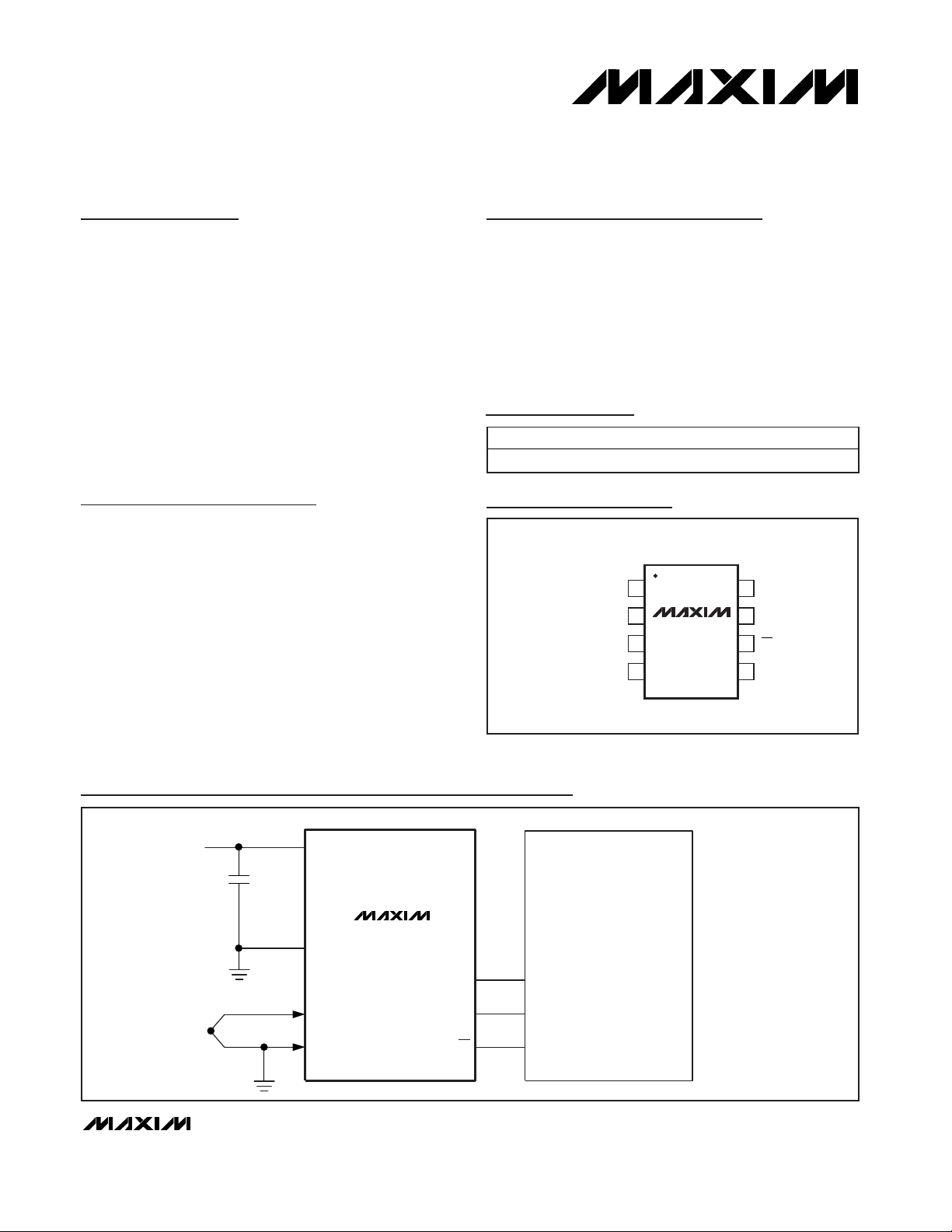
CS
SCKV
CC
1
2
87N.C.
SOT-
T+
GND
SO
TOP VIEW
3
4
6
5
MAX6675
Pin Configuration
Vcc
GND
T+
T-
SO
SCK
CS
MICROCONTROLLER
68HC11A8
MISO
SCK
SSB
0.1µF
MAX6675
Typical Application Circuit
19-2235; Rev 1; 3/02
For pricing, delivery, and ordering information, please contact Maxim/Dallas Direct! at
1-888-629-4642, or visit Maxim’s website at www.maxim-ic.com.
Ordering Information
SPI is a trademark of Motorola, Inc.
PART TEMP RANGE PIN-PACKAGE
MAX6675ISA -20°C to +85°C 8 SO

MAX6675
Cold-Junction-Compensated K-Thermocoupleto-Digital Converter (0°C to +1024°C)
2 _______________________________________________________________________________________
ABSOLUTE MAXIMUM RATINGS
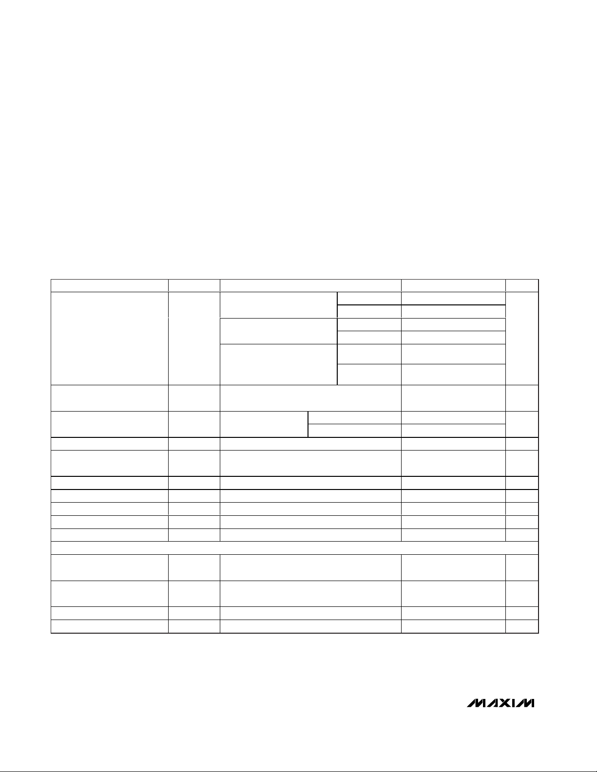
ELECTRICAL CHARACTERISTICS
(VCC= +3.0V to +5.5V, TA= -20°C to +85°C, unless otherwise noted. Typical values specified at +25°C.) (Note 1)
Stresses beyond those listed under “Absolute Maximum Ratings” may cause permanent damage to the device. These are stress ratings only, and functional
operation of the device at these or any other conditions beyond those indicated in the operational sections of the specifications is not implied. Exposure to
absolute maximum rating conditions for extended periods may affect device reliability.
Supply Voltage (VCCto GND) ................................ -0.3V to +6V
SO, SCK,
CS, T-, T+ to GND .......................-0.3V to VCC+ 0.3V
SO Current ........................................................................ 50mA
ESD Protection (Human Body Model) ........................... ±2000V
Continuous Power Dissipation (T
A
= +70°C)
8-Pin SO (derate 5.88mW/°C above +70°C) .............. 471mW
Operating Temperature Range ..........................-20°C to +85°C
Storage Temperature Range ............................-65°C to +150°C
Junction Temperature .................................................... +150°C
SO Package
Vapor Phase (60s) . .....................................................+215°C
Infrared (15s) ..............................................................+220°C
Lead Temperature (soldering, 10s) ............................... +300°C
PARAMETER
SYMBOL
CONDITIONS
MIN
TYP
MAX
UNITS
VCC = +3.3V -5 +5
T
A
= +25°C (Note 2)
V
CC
= +5V -6 +6
VCC = +3.3V -8 +8
T
THERMOCOUPLE
= 0°C to
VCC = +5V -9 +9
VCC = +3.3V -17
Temperature Error
T
THERMOCOUPLE
= +700°C
to +1000°C, T
A
= +25°C
(Note 2)
V
CC
= +5V -19
LSB
Thermocouple Conversion
Constant
µV/LSB
VCC = +3.3V
Cold-Junction
Compensation Error
TA = -20°C to +85°C
(Note 2)
V
CC
= +5V
°C
Resolution
°C
Thermocouple Input
Impedance
60 kΩ
Supply Voltage V
CC
3.0 5.5 V
Supply Current I
CC
0.7 1.5 mA
Power-On Reset Threshold VCC rising 1 2 2.5 V
Power-On Reset Hysteresis 50 mV
Conversion Time (Note 2)
s
SERIAL INTERFACE
Input Low Voltage V
IL
0.3 x
V
Input High Voltage V
IH
0.7 x
V
Input Leakage Current I
LEAK
VIN = GND or V
CC
±5µA
Input Capacitance C
IN
5pF
T
THERMOCOUPLE
+700°C, T
= +700°C,
= +25°C (Note 2)
A
10.25
-3.0 +3.0
-3.0 +3.0
0.25
0.17 0.22
V
CC
+17
+19
V
CC

MAX6675
Cold-Junction-Compensated K-Thermocouple-
to-Digital Converter (0°C to +1024°C)
_______________________________________________________________________________________ 3
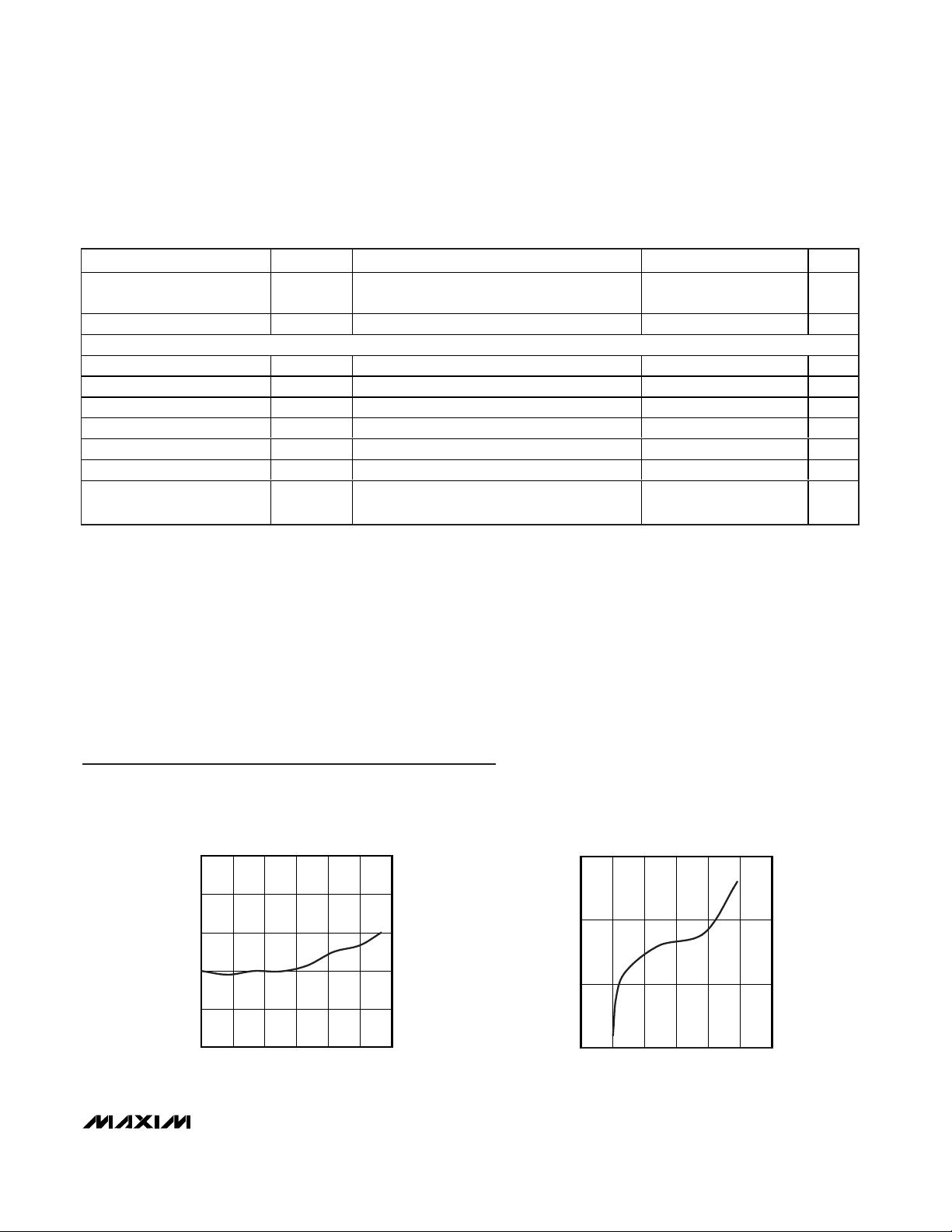
10
8
6
4
2
0
04515 30 60 75 90
OUTPUT CODE ERROR
vs. AMBIENT TEMPERATURE
MAX6675 toc01
TEMPERATURE (°C)
OUTPUT CODE ERROR (LSB)
-5
0
5
10
-10 0 30 50
OUTPUT CODE ERROR
vs. VOLTAGE DIFFERENTIAL
MAX6675 toc02
VOLTAGE DIFFERENTIAL (mV)
OUTPUT CODE ERROR (LSB)
10 20 40
Typical Operating Characteristics
(VCC= +3.3V, TA= +25°C, unless otherwise noted.)
ELECTRICAL CHARACTERISTICS (continued)
(VCC= +3.0V to +5.5V, TA= -20°C to +85°C, unless otherwise noted. Typical values specified at +25°C.) (Note 1)
Note 1: All specifications are 100% tested at T
A
= +25°C. Specification limits over temperature (TA= T
MIN
to T
MAX
) are guaranteed
by design and characterization, not production tested.
Note 2: Guaranteed by design. Not production tested.
PARAMETER
CONDITIONS
UNITS
Output High Voltage V
OH
I
SOURCE
= 1.6mA
V
CC
-
0.4
V
Output Low Voltage V
OL
I
SINK
= 1.6mA 0.4 V
TIMING
Serial Clock Frequency f
SCL
4.3
MHz
SCK Pulse High Width t
CH
ns
SCK Pulse Low Width t
CL
ns
CSB Fall to SCK Rise t
CSS
CL = 10pF
ns
CSB Fall to Output Enable t
DV
CL = 10pF 100 ns
CSB Rise to Output Disable t
TR
CL = 10pF 100 ns
SCK Fall to Output Data
Valid
t
DO
CL = 10pF 100 ns
SYMBOL
MIN TYP MAX
100
100
100
