

General Description
The MAX6666/MAX6667 are high-accuracy, low-cost,
low-power temperature sensors with a single-wire
output. The MAX6666/MAX6667 convert the ambient
temperature into a ratiometric PWM output with temperature information contained in the duty cycle of the output square wave. The MAX6666 has a push-pull output
and the MAX6667 has an open-drain output.
The MAX6666/MAX6667 operate at supply voltages
from +3V to +5.5V. The typical unloaded supply current
at 5.0V is 200µA. Both devices feature a single-wire
output that minimizes the number of pins necessary to
interface with a microprocessor (µP). The output is a
square wave with a nominal frequency of 35Hz (±20%)
at +25°C. The output format is decoded as follows:
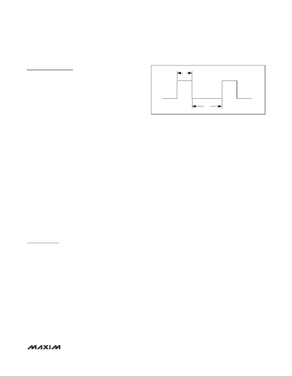
Temperature (°C) = 235 - (400 x t
1
) / t
2
Where t1is fixed with a typical value of 10ms and t2is
modulated by the temperature (Figure 1). The MAX6666/
MAX6667 operate from -40°C to +125°C and are available
in space-saving SOT23 packages.
Applications
Process Control
Industrial
HVAC and Environmental Control
Automotive
µP and µC Temperature Monitoring
Features
o Simple Single-Wire PWM Output
o ±1.0°C Accuracy at +25°C
o High Accuracy
±1°C at T
A
= +30°C
±2.5°C at TA= +10°C to +50°C
o Operate Up to +125°C
o Low 200µA Typical Current Consumption
o Small SOT23 package
MAX6666/MAX6667
High-Accuracy PWM Output Temperature
Sensors
________________________________________________________________
Maxim Integrated Products
1
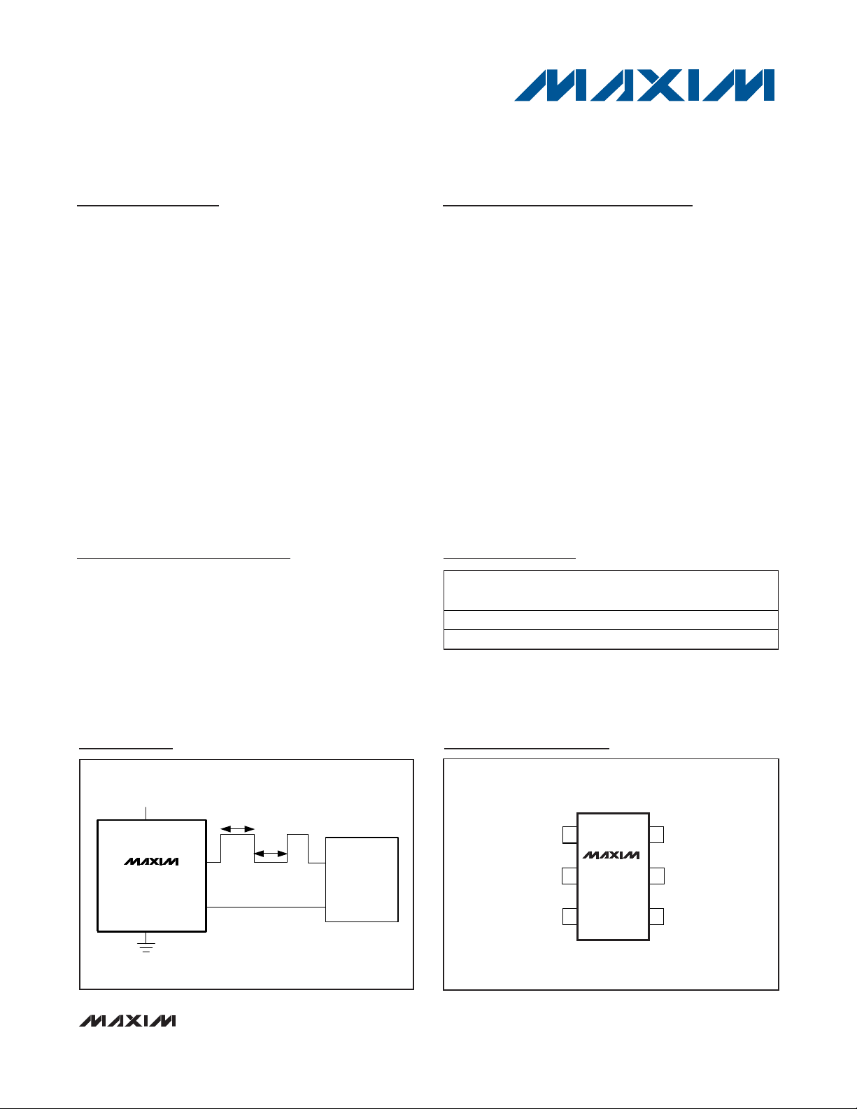
Pin Configuration
Ordering Information
V
CC
+3.3V
GND
DOUT
t
1
t
2
µC
INPUT TO
TIMER/COUNTER
MAX6666
MAX6667
Typical Operating Circuit
19-2138; Rev 3; 8/09
For pricing, delivery, and ordering information, please contact Maxim Direct at 1-888-629-4642,
or visit Maxim’s website at www.maxim-ic.com.
+
Denotes a lead(Pb)-free/RoHS-compliant package.
T = Tape and reel.
PART TEMP RANGE
MAX6666AUT+T -40°C to +125°C
MAX6667AUT+T -40°C to +125°C
PINPACKAGE
6 SOT23
6 SOT23
TOP
MARK
AATF
AATG
+
1
MAX6666
2
MAX6667
34
SOT23
6
I.C.
5
I.C.
I.C.GND
TOP VIEW
D
OUT
V
CC
MAX6666/MAX6667
High-Accuracy PWM Output Temperature
Sensors
2 _______________________________________________________________________________________
ABSOLUTE MAXIMUM RATINGS
ELECTRICAL CHARACTERISTICS
(VCC= +3.0V to +5.5V, TA= -40°C to +125°C, unless otherwise noted. Typical values are at VCC= +3.3V, TA= +25°C.)
Stresses beyond those listed under “Absolute Maximum Ratings” may cause permanent damage to the device. These are stress ratings only, and functional
operation of the device at these or any other conditions beyond those indicated in the operational sections of the specifications is not implied. Exposure to
absolute maximum rating conditions for extended periods may affect device reliability.
(Voltages Referenced to GND)
V
CC
........................................................................-0.3V to +6.0V
D
OUT
MAX6666................................................-0.3V to (VCC+ 0.3V)
MAX6667 ..........................................................-0.3V to + 6.0V
D
OUT
Current ......................................................-1mA to +50mA
Continuous Current into Any Other Terminal....................±20mA
Continuous Power Dissipation (T
A
= +70°C)
6-Pin SOT23 (derate 7.4mW/°C above +70°C)............595mW
Operating Temperature Range .........................-40°C to +150°C
Storage Temperature Range .............................-65°C to +150°C
Junction Temperature......................................................+150°C
Lead Temperature (soldering,10s) ..................................+300°C
PARAMETER SYMBOL CONDITIONS MIN TYP MAX UNITS
Supply Voltage Range V
Supply Current I
Temperature Error VCC = +3.3V
Nominal t1 Pulse Width 10 ms
MAX6666 Output High Voltage IOH = 800µA V
MAX6666 Output Low Voltage IOL = 800µA 0.4 V
MAX6666 Fall Time CL = 100pF, RL = ∞ 80 ns
MAX6666 Rise Time CL = 100pF, RL = ∞ 80 ns
MAX6667 Output Low Voltage
MAX6667 Fall Time CL = 100pF, RL = 10kΩ 40 ns
MAX6667 Output Capacitance CL = 0 15 pF
MAX6667 Output Leakage <0.1 µA
Power-Supply Rejection Ratio PSRR VCC = +3.0V to +5.5V 0.3 1.0 °C/V
CC
CC
VCC = +3.0V to +5.5V 200 500 µA
TA = +30°C -1 +1
T
= +10°C to +50°C -2.5 +2.5
A
T
= 0°C to +100°C -3.8 +3.8
A
T
= -25°C to +125°C -4.8 +4.8
A
= -40°C, VCC = +3.3V -6 +6
T
A
I
= 1.6mA 0.4
SINK
I
= 5.0mA 1.2
SINK
3.0 5.5 V
- 0.4 V
C C
°C
V
MAX6666/MAX6667
High-Accuracy PWM Output Temperature
Sensors
_______________________________________________________________________________________
3
Typical Operating Characteristics
(VCC= +3.3V, TA= +25°C, unless otherwise noted.)
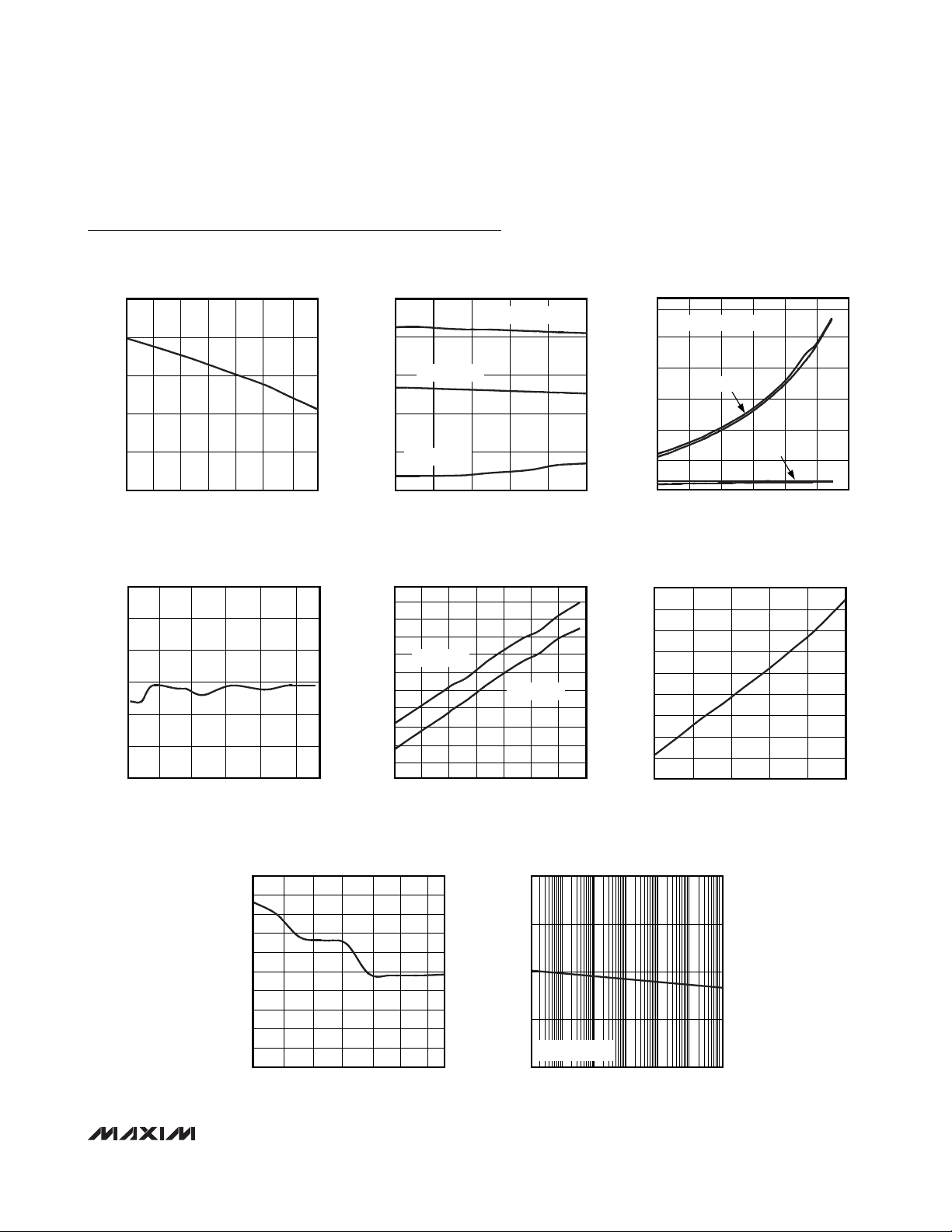
OUTPUT FREQUENCY vs. TEMPERATURE
50
40
30
20
OUTPUT FREQUENCY (Hz)
10
0
-40 10-15 356085110
TEMPERATURE (°C)
MAX6666/7 toc01
OUTPUT FREQUENCY (Hz)
OUTPUT ACCURACY
vs. TEMPERATURE
MAX6666/7 toc04
210
200
190
180
170
160
150
140
SUPPLY CURRENT (µA)
130
120
110
100
3
2
1
0
-1
OUTPUT ACCURACY (°C)
-2
-3
-40 20 50-10 80 110
TEMPERATURE (°C)
OUTPUT FREQUENCY vs. SUPPLY VOLTAGE
45
40
TEMP = +25°C
35
30
25
TEMP = -40°C
20
3.0 4.03.5 4.5 5.0 5.5
SUPPLY VOLTAGE (V)
SUPPLY CURRENT
vs. TEMPERATURE
VCC = +5.5V
-55 5 35-25
TEMP = +125°C
VCC = +3.3V
65
TEMPERATURE (°C)
95 125 155
MAX6666/7 toc02
MAX6666/7 toc05
SUPPLY CURRENT (µA)
T1 AND T2 TIMES
vs. TEMPERATURE
39
TWO TYPICAL PARTS
34
29
T
24
TIME (ms)
19
14
9
-40 20 50-10 80 110 140
2
T
1
TEMPERATURE (°C)
SUPPLY CURRENT vs. SUPPLY VOLTAGE
158
156
154
152
150
148
146
144
142
140
3.0 4.03.5 4.5 5.0 5.5
SUPPLY VOLTAGE (V)
MAX6666/7 toc03
MAX6666/7 toc06
POWER-SUPPLY REJECTION RATIO
vs. TEMPERATURE
0.50
0.45
0.40
0.35
0.30
0.25
PSRR (°C/V)
0.20
0.15
0.10
0.05
0
-40 -15 10 35 60 85 110
TEMPERATURE (°C)
MAX6666/7 toc07
1.0
0.5
CHANGE IN TEMPERATURE (°C)
-0.5
-1.0
POWER-SUPPLY REJECTION
vs. FREQUENCY
MAX6666/7 toc08
0
VAC = 100mVp-p
0.01 10 100 1k0.1 1 10k
FREQUENCY (Hz)
MAX6666/MAX6667
High-Accuracy PWM Output Temperature
Sensors
4 _______________________________________________________________________________________
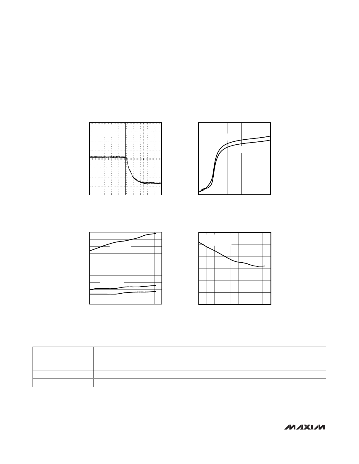
Typical Operating Characteristics (continued)
(VCC= +3.3V, TA= +25°C, unless otherwise noted.)
40ns/div
MAX6666
OUTPUT FALL TIME
MAX6666/7 toc09
1V/div
C
LOAD
= 100pF
R
L
= 100kΩ
0
400
200
800
600
1000
1200
MAX6666
OUTPUT RISE AND FALL TIMES
vs. CAPACITIVE LOADS
MAX6666/7 toc10
C
LOAD
(pF)
TIME (ns)
0 600300 900 1200 1500
RISE TIME
FALL TIME
0
0.2
0.1
0.4
0.3
0.6
0.5
0.7
0.9
0.8
1.0
-40 0 20 40-20 60 80 100 120 140
OUTPUT LOW VOLTAGE
vs. TEMPERATURE
MAX6666/7 toc11
TEMPERATURE (°C)
OUTPUT LOW VOLTAGE (V)
I
SINK
= 5mA
I
SINK
= 1.5mA
I
SINK
= 1mA
Pin Description
3.00
3.05
3.10
3.15
3.20
3.25
3.30
-40 0-20 20 40 60 80 100 120 140
OUTPUT HIGH VOLTAGE
VS. TEMPERATURE
MAX6666/7 toc12
TEMPERATURE (°C)
OUTPUT HIGH VOLTAGE (V)
VCC = +3.3V
I
SOURCE
= 800µA
PIN NAME FUNCTION
1D
2VCCSupply Voltage
3 GND Ground
4, 5, 6 I.C. Internally Connected. Leave I.C. unconnected or connect to GND.
OUT
Digital Output Pin. The pulse width of the output waveform is modulated by the temperature.
Detailed Description
The MAX6666/MAX6667 are high-accuracy, low-cost,
low current (200µA typ) temperature sensors ideal for
interfacing with µCs or µPs. The MAX6666/MAX6667
convert the ambient temperature into a ratiometric
PWM output at a nominal frequency of 35Hz (±20%) at
+25°C.
The time periods, t
1
(high) and t2(low) (Figure 1), are
easily read by the µP’s timer/counter port. To calculate
the temperature, use the expression below:
Temperature (°C) = +235 - (400 x t1) / t
2
The µC or µP measures the output of the MAX6666/
MAX6667 by counting t1and t2and computing the
temperature based on their ratio. The resolution of the
count is a function of the processor clock frequency
and the resolution of the counter. The MAX6666/
MAX6667 have a resolution of approximately 11 bits.
Always use the same clock for t1and t2counters so
that the temperature is strictly based on a ratio of the
two times, thus eliminating errors due to different
clocks’ frequencies.
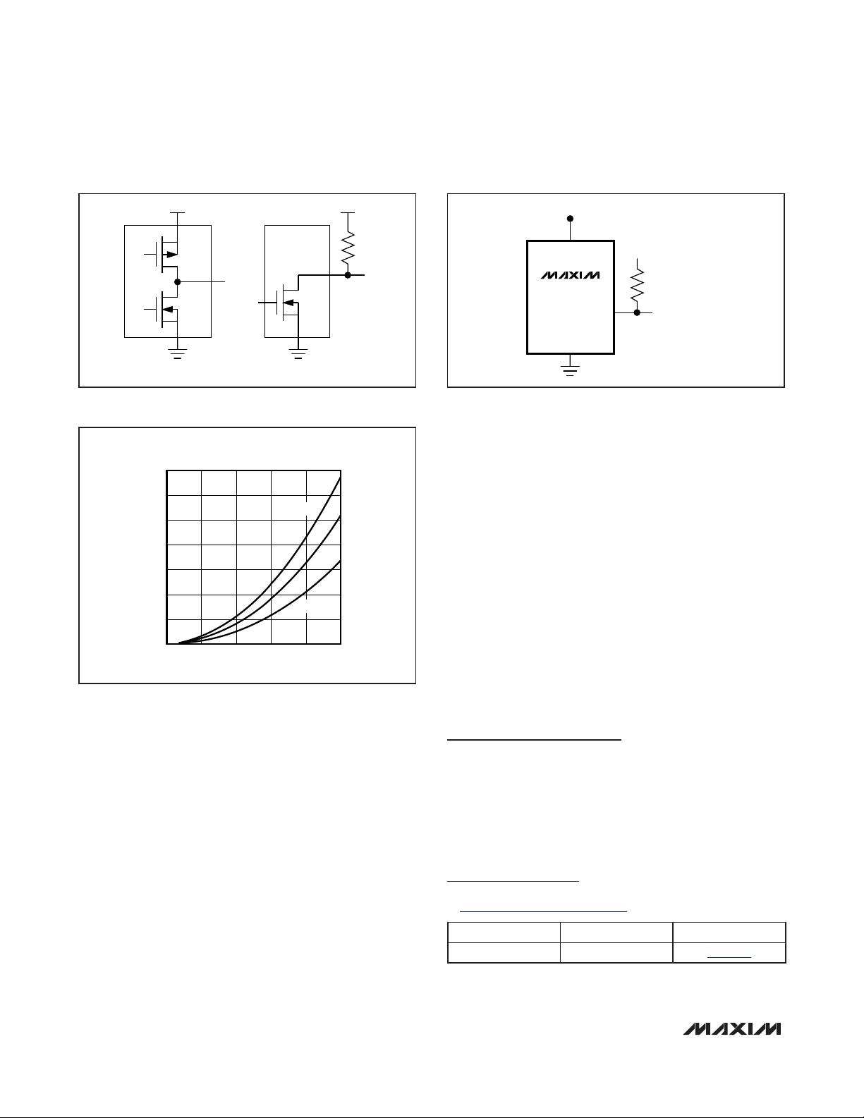
The MAX6666 (Figure 2a) has a push-pull output and
provides rail-to-rail output drive. The ability to source
and sink current allows the MAX6666 to drive capacitive loads up to 10nF with less than 1°C error.
The MAX6667 (Figure 2b) has an open-drain output.
The output capacitance should be minimized in
MAX6667 applications because the sourcing current is
set by the pullup resistor. If the output capacitance
becomes too large, lengthy rise and fall times distort
the pulse width, resulting in inaccurate measurements.
Applications Information
Accurate temperature monitoring requires a good thermal contact between the MAX6666/MAX6667 and the
object being monitored. A precise temperature measurement depends on the thermal resistance between
the object being monitored and the MAX6666 die. Heat
flows in and out of plastic packages primarily through
the leads. For the best thermal contact, connect all
unused pins to ground. If the sensor is intended to
measure the temperature of a heat-generating component on the circuit board, mount the device as close as
possible to that component and share the ground
traces (if they are not too noisy) with the component.
This maximizes the heat transfer from the component to
the sensor.
Power-Supply Bypassing
The MAX6666/MAX6667 operate from a +3V to +5.5V
supply. If a noisy power-supply line is used, bypass
VCCto GND with a 0.1µF capacitor.
Power Supply from µP Port Pin
The low quiescent current of the MAX6666/MAX6667
enables it to be powered from a logic line, which meets
the requirements for supply voltage range. This provides a simple shutdown function to totally eliminate
quiescent current by taking the logic line low. The logic
line must be able to withstand the 0.1µF power-supply
bypass capacitance.
Galvanic Isolation
Use an optocoupler to isolate the MAX6666/MAX6667
whenever a high common-mode voltage is present.
Because some optocouplers have turn-off times that
are much longer than their turn-on times, choose an
optocoupler with equal turn-on and turn-off times.
Unequal turn-on/turn-off times produce an error in the
temperature reading.
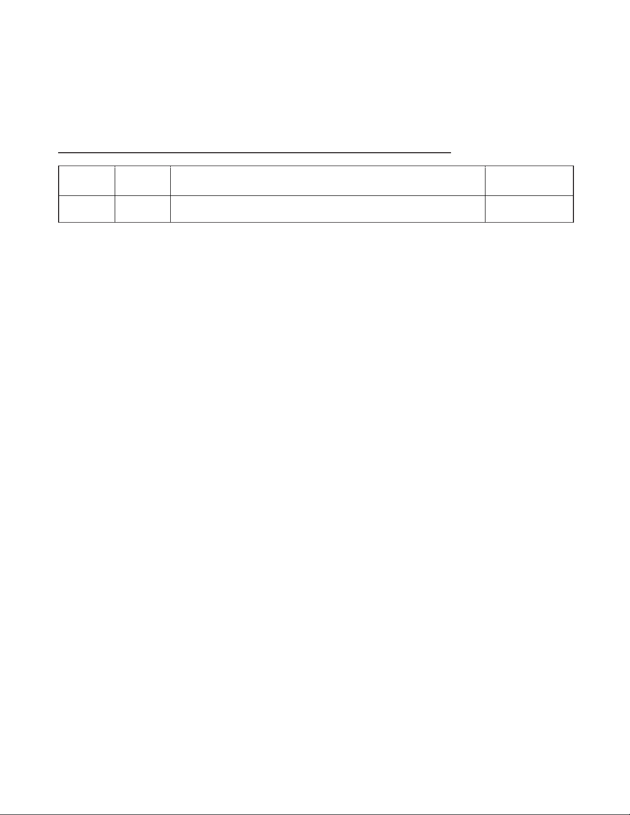
Thermal Considerations
Self-heating may cause the temperature measurement
accuracy of the MAX6666/MAX6667 to degrade in
some applications. The quiescent dissipation and the
power dissipated by the digital output may cause
errors in obtaining the accurate temperature measurement. The temperature errors depend on the thermal
conductivity of the package (SOT23, 140°C/W), the
mounting technique, and the airflow. Static dissipation
in the MAX6666/MAX6667 is typically 4.5mW operating
at 5V with no load. As a worst-case example, consider
the MAX6667 and its maximum rated load of 5mA and
assume a maximum output voltage of 0.8V adds 4mW
power dissipation. Use Figure 3 to estimate the temperature error.
MAX6666/MAX6667
High-Accuracy PWM Output Temperature
Sensors
_______________________________________________________________________________________ 5
Figure 1. MAX6666/MAX6667 PWM Output
t
1
t
2
MAX6666/MAX6667
Low-Voltage Logic
Use the MAX6667 open-drain output to drive low-voltage devices. As shown in Figure 4, connect a pullup
resistor from the low-voltage logic supply to the
MAX6667 output. Limit the resistor’s current to about
1mA, thus maintaining an output low logic level of less
than 200mV.
Chip Information
PROCESS: BiCMOS
High-Accuracy PWM Output Temperature
Sensors
6 _______________________________________________________________________________________
Figure 2. MAX6666/MAX6667 Output Configuration
Figure 4. Low-Voltage Logic
Figure 3. MAX6666 Temperature Error Due to Load Current
Package Information
For the latest package outline information and land patterns, go
to www.maxim-ic.com/packages
.
PACKAGE TYPE PACKAGE CODE DOCUMENT NO.
6 SOT23 U6F+6
21-0058
V
CC
P
DOUT
N
(a) (b)
N
TEMPERATURE ERROR vs. LOAD CURRENT
3.5
3.0
2.5
2.0
1.5
1.0
TEMPERATURE ERROR (°C)
0.5
MAX6666
µMAX
SO
SOT23-6
V
CC
DOUT
+3.3V
MAX6667
GND
DOUT
2.5V
5.1kΩ
TO LOGIC GATE INPUT
0
0462810
LOAD CURRENT (mA)
MAX6666/MAX6667
High-Accuracy PWM Output Temperature
Sensors
Maxim cannot assume responsibility for use of any circuitry other than circuitry entirely embodied in a Maxim product. No circuit patent licenses are
implied. Maxim reserves the right to change the circuitry and specifications without notice at any time.
Maxim Integrated Products, 120 San Gabriel Drive, Sunnyvale, CA 94086 408-737-7600 _____________________
7
© 2009 Maxim Integrated Products Maxim is a registered trademark of Maxim Integrated Products, Inc.
Revision History
REVISION
NUMBER
3 8/09
REVISION
DATE
DESCRIPTION
Updated Ordering Information, Pin Configuration, Absolute Maximum Ratings,
and Pin Description sections
PAGES
CHANGED
1, 2, 4
 Loading...