

General Description
The MAX6657/MAX6658/MAX6659 are precise, twochannel digital temperature sensors. Each accurately
measures the temperature of its own die and one
remote PN junction, and reports the temperature in digital form on a 2-wire serial interface. The remote junction
can be a diode-connected transistor like the low-cost
NPN type 2N3904 or 2N3906 PNP type. The remote
junction can also be a common-collector PNP, such as
a substrate PNP of a microprocessor.
The 2-wire serial interface accepts standard System
Management Bus (SMBus™) commands such as Write
Byte, Read Byte, Send Byte, and Receive Byte to read
the temperature data and program the alarm thresholds
and conversion rate. The MAX6657/MAX6658/
MAX6659 can function autonomously with a programmable conversion rate, which allows the control of supply current and temperature update rate to match
system needs. For conversion rates of 4Hz or less, the
temperature is represented in extended mode as 10
bits + sign with a resolution of 0.125°C. When the conversion rate is faster than 4Hz, output data is 7 bits +
sign with a resolution of 1°C. The MAX6657/
MAX6658/MAX6659 also include an SMBus timeout
feature to enhance system reliability.
Remote accuracy is ±1°C between +60°C and +100°C
with no calibration needed. The MAX6657 measures
temperatures from 0°C to +125°C and the MAX6658/
MAX6659 from -55°C to +125°C. The MAX6659 has the
added benefit of being able to select one of three
addresses through an address pin, and a second overtemperature alarm pin for greater system reliability.
Applications
Desktop Computers Workstations
Notebook Computers
Servers
Features
o Dual Channel Measures Remote and Local
Temperature
o 11-Bit, +0.125°C Resolution
o High Accuracy ±1°C (max) from +60°C to +100°C
(Remote)
o No Calibration Required
o Programmable Under/Overtemperature Alarms
o Programmable Conversion Rate
(0.0625Hz to 16Hz)
o SMBus/I
2
C-Compatible Interface
o Two Alarm Outputs: ALERT and OVERT1
(MAX6657 and MAX6658)
o Three Alarm Outputs: ALERT, OVERT1,
and OVERT2 (MAX6659)
o Compatible with 65nm Process Technology
(Y Versions)
MAX6657/MAX6658/MAX6659
±1°C, SMBus-Compatible Remote/Local Temperature
Sensors with Overtemperature Alarms
________________________________________________________________
Maxim Integrated Products
1
19-2034; Rev 5; 10/10
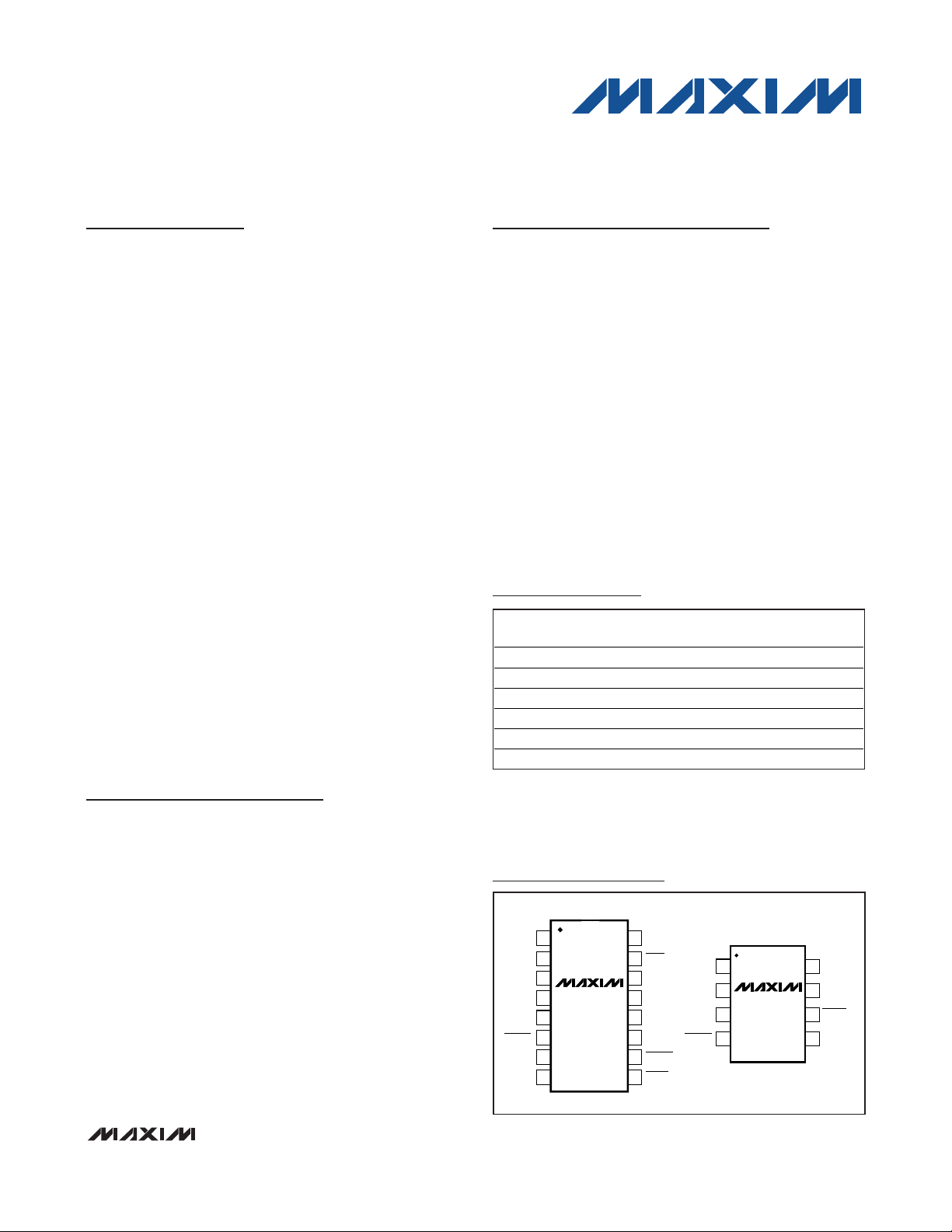
Ordering Information
SMBus is a trademark of Intel Corp.
16
15
14
13
12
11
10
9
1
2
3
4
5
6
7
8
V
CC
N.C.
STBY
SMBCLK
N.C.
SMBDATA
N.C.
OVERT2
ALERT
TOP VIEW
MAX6659
QSOP
N.C.
DXP
OVERT1
DXN
ADD
GND
GND
ALERT
GNDOVERT1
1
2
87SMBCLK
SMBDATADXP
DXN
V
CC
SO
3
4
6
5
MAX6657
MAX6658
Pin Configurations
For pricing, delivery, and ordering information, please contact Maxim Direct at 1-888-629-4642,
or visit Maxim’s website at www.maxim-ic.com.
Typical Operating Circuit appears at the end of the data
sheet.
Ordering Information continued at end of data sheet.
Note: All devices are specified over the -55°C to +125°C oper-
ating temperature range.
+
Denotes a lead(Pb)-free/RoHS-compliant package.
T = Tape and reel.
PART
MAX6657MSA 0°C to +125°C 8 SO
MAX6657MSA+ 0°C to +125°C 8 SO
MAX6657MSA-T 0°C to +125°C 8 SO
MAX6657MSA+T 0°C to +125°C 8 SO
MAX6657YMSA+ 0°C to +125°C 8 SO
MAX6657YMSA+T 0°C to +125°C 8 SO
MEASURED TEMP
RANGE
PIN-PACKAGE

MAX6657/MAX6658/MAX6659
2 _______________________________________________________________________________________
ABSOLUTE MAXIMUM RATINGS
Stresses beyond those listed under “Absolute Maximum Ratings” may cause permanent damage to the device. These are stress ratings only, and functional
operation of the device at these or any other conditions beyond those indicated in the operational sections of the specifications is not implied. Exposure to
absolute maximum rating conditions for extended periods may affect device reliability.
(All voltages referenced to GND.)
V
CC
..........................................................................-0.3V to +6V
DXP ............................................................-0.3V to (V
CC
+ 0.3V)
DXN ......................................................................-0.3V to +0.8V
SMBCLK, SMBDATA, ALERT, OVERT1,
OVERT2 ..............................................................-0.3V to +6V
SMBDATA, ALERT, OVERT1, OVERT2
Current ..........................................................-1mA to +50mA
DXN Current ......................................................................±1mA
Continuous Power Dissipation (T
A
= +70°C)
8-Pin SO (derate 5.9mW/°C above +70°C) .................471mW
16-Pin QSOP (derate 8.3mW/°C above +70°C) ..........664mW
Junction Temperature .....................................................+150°C
Storage Temperature Range ............................-65°C to +150°C
Lead Temperature (soldering, 10s) ................................+300°C
Soldering Temperature (reflow)
Lead(Pb)-free ..............................................................+260°C
Containing lead(Pb) ....................................................+240°C
ELECTRICAL CHARACTERISTICS
(VCC= +3.0V to +5.5V, TA= 0°C to +125°C, unless otherwise specified. Typical values are at VCC= +3.3V and TA= +25°C.)
±1°C, SMBus-Compatible Remote/Local Temperature
Sensors with Overtemperature Alarms
PARAMETER SYMBOL CONDITIONS MIN TYP MAX UNITS
Temperature Resolution,
Legacy Mode
Temperature Resolution,
Extended Mode
TRJ = +60°C to +100°C, VCC = +3.3V
Remote Temperature Error
(MAX6657, MAX6657Y)
Local Temperature Error
(MAX6657)
Remote Temperature Error
(MAX6658/MAX6659/
MAX6658Y/MAX6659Y)
Local Temperature Error
(MAX6658/MAX6659)
Local Temperature Error
(MAX665_Y)
Line Regulation 3.0V ≤ VCC ≤ 5.5V 0.2 0.6 m°C/V
Supply Voltage Range V
Undervoltage Lockout Threshold UVLO Falling edge of VCC disables ADC 2.60 2.80 2.95 V
Undervoltage Lockout Hysteresis 90 mV
Power-On Reset (POR) Threshold VCC, falling edge 1.5 2.0 2.5 V
POR Threshold Hysteresis 90 mV
Standby Supply Current SMBus static 3 10 µA
Operating Current During conversion 0.5 1.0 mA
(Note 1)
TRJ = 0°C to +100°C, VCC = +3.3V (Note 1) -3.0 +3.0
= 0°C to +125°C, VCC = +3.3V (Note 1) -5.0 +5.0
T
RJ
TA = +60°C to +100°C, VCC = +3.3V -2.0 +2.0
TA = 0°C to +100°C, VCC = +3.3V -3.0 +3.0
= 0°C to +125°C, VCC = +3.3V -5.0 +5.0
T
A
TRJ = +60°C to +100°C, VCC = +3.3V
(Note 1)
TRJ = 0°C to +100°C, VCC = +3.3V (Note 1) -3.0 3.0
T
= -55°C to +125°C, VCC = +3.3V (Note 1) -5.0 +5.0
RJ
TA = +60°C to +100°C, VCC = +3.3V -2.0 +2.0
TA = 0°C to +100°C, VCC = +3.3V -3.0 +3.0
= -55°C to +125°C, VCC = +3.3V (Note 2) -5.0 +5.0
T
A
TA = +60°C to +100°C, VCC = +3.3V -3.8
TA = 0°C to +100°C, VCC = +3.3V -4.0
T
= 0°C to +125°C, VCC = +3.3V -4.4
A
CC
1°C
8 Bits
0.125 °C
11 Bits
-1.0 +1.0
-1.0 1.0
3.0 5.5 V
°C
°C
°C
°C
°C
MAX6657/MAX6658/MAX6659
_______________________________________________________________________________________ 3
Note 1: TA= +25°C to +85°C.
Note 2: If both the local and the remote junction are below T
A
= -20°C, then VCC> 3.15V.
Note 3: For conversion rates of 4Hz or slower, the conversion time doubles.
Note 4: Timing specifications guaranteed by design.
Note 5: The serial interface resets when SMBCLK is low for more than t
TIMEOUT
.
Note 6: A transition must internally provide at least a hold time to bridge the undefined region (300ns max) of SMBCLK's falling edge.
ELECTRICAL CHARACTERISTICS (continued)
(VCC= +3.0V to +5.5V, TA= 0°C to +125°C, unless otherwise specified. Typical values are at VCC= +3.3V and TA= +25°C.)
±1°C, SMBus-Compatible Remote/Local Temperature
Sensors with Overtemperature Alarms
Average Operating Current
SMBus-COMPATIBLE INTERFACE (SMBCLK, SMBDATA, STBY)
SMBus-COMPATIBLE TIMING (Note 4)
PARAMETER SYMBOL CONDITIONS MIN TYP MAX UNITS
0.25 conversions/s 40 70
2 conversions/s 150 250
Conversion Time t
Conversion Timing Error ±25 %
DXP and DXN Leakage Current In standby mode 100 nA
Remote-Diode Source Current I
(ALERT, OVERT)
Output Low Sink Current
Output High Leakage Current VOH = 5.5V 1 µA
Logic Input Low Voltage V
Logic Input High Voltage V
Input Leakage Current I
Output Low Sink Current I
Input Capacitance C
Serial-Clock Frequency f
Bus Free Time Between STOP
and START Condition
START Condition Setup Time 4.7 µs
Repeat START Condition Setup
Time
START Condition Hold Time t
STOP Condition Setup Time t
Clock Low Period t
Clock High Period t
Data Setup Time t
Receive SCL/SDA Rise Time t
Receive SCL/SDA Fall Time t
Pulse Width of Spike Suppressed t
SMBus Timeout SMBDATA low period for interface reset 25 37 45 ms
CONV
LEAK
SCL
t
BUF
t
SU:STA
HD:STA
SU:STO
LOW
HIGH
HD:DAT
From stop bit to conversion completed
(Note 4)
High level 80 100 120
RJ
Low level 8 10 12
VOL = 0.4V 1
V
= 0.6V 6
OL
IL
VCC = +3.0V 2.2
IH
VCC = +5.5V 2.4
VIN = V
VOL = 0.6V 6 mA
OL
IN
(Note 5) 100 kHz
90% to 90% 50 ns
10% of SMBDATA to 90% of SMBCLK 4 µs
90% of SMBCLK to 90% of SMBDATA 4 µs
10% to 10% 4.7 µs
90% to 90% 4 µs
(Note 6) 0 µs
R
F
SP
GND
or V
CC
95 125 156 ms
0.8 V
±1 µA
5pF
4.7 µs
1µs
300 ns
050ns
µA
µA
mA
V
MAX6657/MAX6658/MAX6659
4 _______________________________________________________________________________________
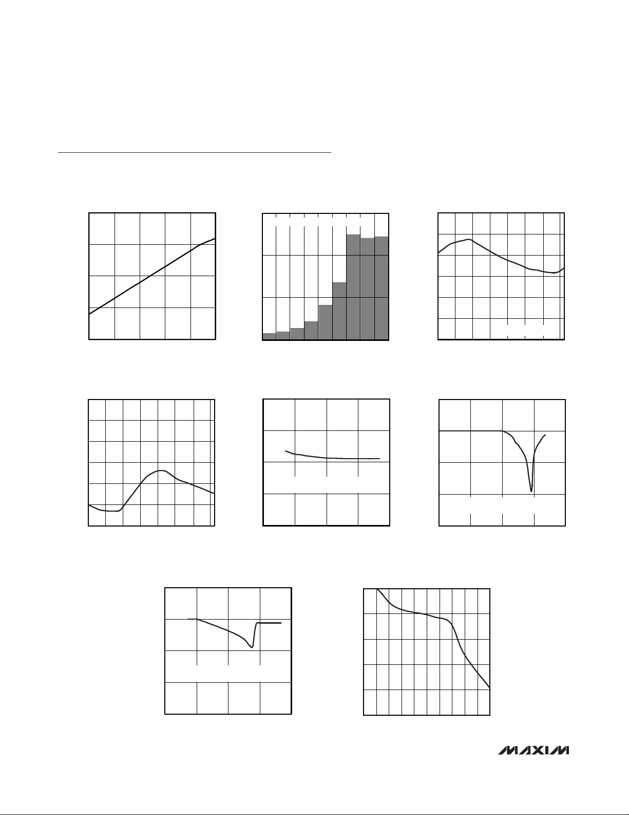
Typical Operating Characteristics
(VCC= +3.3V, TA= +25°C, unless otherwise noted.)
4.5
4.0
3.5
3.0
2.5
3.0 4.03.5 4.5 5.0 5.5
STANDBY SUPPLY CURRENT
vs. SUPPLY VOLTAGE
MAX6657 toc01
SUPPLY VOLTAGE (V)
STANDBY SUPPLY CURRENT (µA)
0.063 0.5 10.125 0.25 2 4 8 16
OPERATING SUPPLY CURRENT
vs. CONVERSION RATE
MAX6657 toc02
CONVERSION RATE (Hz)
OPERATING SUPPLY CURRENT (µA)
0
200
400
600
8Hz AND 16Hz ARE 1°C RESOLUTION
-3
-2
-1
0
1
2
3
-55 -5-30 20 45 70 95 120
MAX6659
REMOTE TEMPERATURE ERROR
vs. REMOTE-DIODE TEMPERATURE
MAX6657 toc03
TEMPERATURE (°C)
TEMPERATURE ERROR (°C)
FAIRCHILD 2N3906
-3
-2
-1
0
1
2
3
-55 -5-30 20 45 70 95 120
LOCAL TEMPERATURE ERROR
vs. DIE TEMPERATURE
MAX6657 toc04
TEMPERATURE (°C)
TEMPERATURE ERROR (°C)
1
0
-1
-2
-3
10k 1M100k 10M 100M
TEMPERATURE ERROR vs.
POWER-SUPPLY NOISE FREQUENCY
MAX6657 toc05
FREQUENCY (Hz)
TEMPERATURE ERROR (°C)
VIN = SQUARE WAVE APPLIED TO V
CC
WITH NO 0.1µF VCC CAPACITOR
1
0
-1
-2
-3
0.01k 100k1k 10M 1G
TEMPERATURE ERROR vs.
COMMON-MODE NOISE FREQUENCY
MAX6657 toc06
FREQUENCY (Hz)
TEMPERATURE ERROR (°C)
VIN = AC-COUPLED TO DXN
V
IN
= 100mVp-p
1
0
-1
-2
-3
10k 1M100k 10M 100M
TEMPERATURE ERROR vs.
DIFFERENTIAL-MODE NOISE FREQUENCY
MAX6657 toc07
FREQUENCY (Hz)
TEMPERATURE ERROR (°C)
VIN = 10mV
P-P
SQUARE WAVE
APPLIED TO DXP-DXN
-5
-4
-3
-2
-1
0
0405020 3010 60 70 80 90 100
TEMPERATURE ERROR vs.
DXP-DXN CAPACITANCE
MAX6657 toc08
DXP-DXN CAPACITANCE (nF)
TEMPERATURE ERROR (°C)
±1°C, SMBus-Compatible Remote/Local Temperature
Sensors with Overtemperature Alarms

MAX6657/MAX6658/MAX6659
_______________________________________________________________________________________ 5
Pin Description
±1°C, SMBus-Compatible Remote/Local Temperature
Sensors with Overtemperature Alarms
PIN
MAX6657
MAX6658
11V
2 3 DXP
34DXN
46OVERT1
5 7, 8 GND Ground
69ALERT
7 12 SMBDATA SMBus Serial-Data Input/Output, Open-Drain
8 14 SMBCLK SMBus Serial-Clock Input
— 5 ADD
—10OVERT2
—15STBY
— 2, 11, 13, 16 N.C. Not internally connected. Do not make connections to these pins.
MAX6659
NAME FUNCTION
Supply Voltage Input, +3V to +5.5V. Bypass to GND with a 0.1µF capacitor. A 200Ω
CC
series resistor is recommended but not required for additional noise filtering. See
Typical Operating Circuit.
Combined Remote-Diode Current Source and A/D Positive Input for Remote-Diode
Channel. DO NOT LEAVE DXP UNCONNECTED; connect DXP to DXN if no remote
diode is used. Place a 2200pF capacitor between DXP and DXN for noise filtering.
Combined Remote-Diode Current Sink and A/D Negative Input. DXN is internally
biased to one diode drop above ground.
Overtemperature Active-Low Output, Open-Drain. Output is logic low only when
temperature is above the software programmed threshold.
SMBus Alert (Interrupt) Active-Low Output, Open-Drain. Asserts when temperature
exceeds user-set limits (high or low temperature). Stays asserted until acknowledged
by either reading the Status register or by successfully responding to an Alert
ALERT
Response address. See
SMBus Address-Select Pin. The MAX6659 is set to one of three available addresses
(connect to V
Overtemperature Active-Low Output, Open-Drain. Output is logic low only when
temperature is above the software programmed threshold.
Hardware Standby Input. Temperature and comparison threshold data are retained in
standby mode. If STBY is low, the IC is put into standby mode.
, GND, or leave open). See Slave Addresses section.
CC
Interrupts.

MAX6657/MAX6658/MAX6659
Detailed Description
The MAX6657/MAX6658/MAX6659 are temperature
sensors designed to work in conjunction with a microprocessor or other intelligence in thermostatic,
process-control, or monitoring applications. Communication with the MAX6657/MAX6658/MAX6659
occurs through the SMBus serial interface and dedicated alert pins. Two independent overtemperature alarms
(OVERT1 and OVERT2) are asserted if their software
programmed temperature thresholds are exceeded.
OVERT1 and OVERT2 can be connected to fans, a system shutdown, or other thermal management circuitry.
The MAX6657/MAX6658/MAX6659 convert temperatures to digital data either at a programmed rate or a
single conversion. Conversions have a 0.125°C resolution (extended resolution) or 1°C resolution (legacy resolution). Extended resolution represents temperature as
10 bits + sign bit and is available for autonomous conversions that are 4Hz and slower and single-shot conversions. Legacy resolution represents temperature as
7 bits + sign bit and allows for faster autonomous conversion rates of 8Hz and 16Hz.
ADC and Multiplexer
The averaging ADC integrates over a 60ms period
(each channel, typically, in the 7-bit + sign legacy
mode). Using an averaging ADC attains excellent noise
rejection.
The multiplexer automatically steers bias currents
through the remote and local diodes. The ADC and
associated circuitry measure each diode’s forward voltage and compute the temperature based on this voltage. If the remote channel is not used, connect DXP to
DXN. Do not leave DXP and DXN unconnected. When a
conversion is initiated, both channels are converted
6 _______________________________________________________________________________________
Functional Diagram
±1°C, SMBus-Compatible Remote/Local Temperature
Sensors with Overtemperature Alarms
V
CC
MAX6657
MAX6658
MAX6659
2
DXP
DXN
ALERT
Q
OVERT1
Q
(OVERT2)
Q
MUX
REMOTE
LOCAL
DIODE
FAULT
S
R
S
R
S
R
MAX6659 ONLY
ADC
REGISTER BANK
COMMAND BYTE
REMOTE TEMPERATURE
LOCAL TEMPERATURE
ALERT THRESHOLD
ALERT RESPONSE
ADDRESS
OVERT1 THRESHOLD
(OVERT2 THRESHOLD)
8
8
CONTROL
LOGIC
SMBus
READ
WRITE
7
ADDRESS
DECODER
( ) ARE FOR MAX6659 ONLY
(STBY)
SMBDATA
SMBCLK
(ADD)

whether they are used or not. The DXN input is biased
at one VBEabove ground by an internal diode to set up
the ADC inputs for a differential measurement.
Resistance in series with the remote diode causes
about +1/2°C error per ohm.
A/D Conversion Sequence
A conversion sequence consists of a local temperature
measurement and a remote temperature measurement.
Each time a conversion begins, whether initiated automatically in the free-running autoconvert mode
(RUN/STOP = 0) or by writing a “one-shot” command,
both channels are converted, and the results of both
measurements are available after the end of conversion. A BUSY status bit in the Status register shows that
the device is actually performing a new conversion. The
results of the previous conversion sequence are still
available when the ADC is busy.
Remote-Diode Selection
The MAX6657/MAX6658/MAX6659 can directly measure the die temperature of CPUs and other ICs that
have on-board temperature-sensing diodes (see
Typical Operating Circuit
) or they can measure the temperature of a discrete diode-connected transistor. The
type of remote diode used is set by bit 5 of the
Configuration Byte. If bit 5 is set to zero, the remote
sensor is a diode-connected transistor, and if bit 5 is set
to 1, the remote sensor is a substrate or common collector PNP transistor. For best accuracy, the discrete transistor should be a small-signal device with its collector
and base connected together. Accuracy has been
experimentally verified for all the devices listed in Table 1.
The transistor must be a small-signal type with a relatively high forward voltage; otherwise, the A/D input
voltage range can be violated. The forward voltage at
the highest expected temperature must be greater than
0.25V at 10µA, and at the lowest expected temperature, forward voltage must be less than 0.95V at 100µA.
Large power transistors must not be used. Also, ensure
that the base resistance is less than 100Ω. Tight specifications for forward current gain (50 < β < 150, for
example) indicate that the manufacturer has good
process controls and that the devices have consistent
V
BE
characteristics.
Thermal Mass and Self-Heating
When sensing local temperature, these devices are
intended to measure the temperature of the PC board
to which they are soldered. The leads provide a good
thermal path between the PC board traces and the die.
Thermal conductivity between the die and the ambient
air is poor by comparison, making air temperature measurements impractical. Because the thermal mass of
the PC board is far greater than that of the MAX6657/
MAX6658/MAX6659, the devices follow temperature
changes on the PC board with little or no perceivable
delay.
When measuring the temperature of a CPU or other IC
with an on-chip sense junction, thermal mass has virtually no effect; the measured temperature of the junction
tracks the actual temperature within a conversion cycle.
When measuring temperature with discrete remote sensors, smaller packages (i.e., a SOT23) yield the best
thermal response times. Take care to account for thermal gradients between the heat source and the sensor,
and ensure that stray air currents across the sensor
package do not interfere with measurement accuracy.
Self-heating does not significantly affect measurement
accuracy. Remote-sensor self-heating due to the diode
current source is negligible. For the local diode, the
worst-case error occurs when autoconverting at the
fastest rate and simultaneously sinking maximum current at the ALERT output. For example, with VCC=
+5.0V, a 16Hz conversion rate and ALERT sinking
1mA, the typical power dissipation is:
VCCx 450µA + 0.4V x 1mA = 2.65mW
θ
J-A
for the 8-pin SO package is about +170°C/W, so
assuming no copper PC board heat sinking, the resulting temperature rise is:
∆T = 2.65mW x +170°C/W = +0.45°C
Even under these engineered circumstances, it is difficult to introduce significant self-heating errors.
ADC Noise Filtering
The integrating ADC used has good noise rejection for
low-frequency signals such as 60Hz/120Hz power-supply hum. In noisy environments, high-frequency noise
reduction is needed for high-accuracy remote mea-
MAX6657/MAX6658/MAX6659
_______________________________________________________________________________________ 7
Note: Transistors must be diode connected (base shorted to
collector).
Table 1. Remote-Sensor Transistor
±1°C, SMBus-Compatible Remote/Local Temperature
Sensors with Overtemperature Alarms
MANUFACTURER MODEL NUMBER
Central Semiconductor (USA) CMPT3904
Fairchild Semiconductor (USA) 2N3904, 2N3906
On Semiconductor (USA) 2N3904, 2N3906
Rohm Semiconductor (USA) SST3904
Samsung (Korea) KST3904-TF
Siemens (Germany) SMBT3904
Zetex (England) FMMT3904CT-ND

MAX6657/MAX6658/MAX6659
surements. The noise can be reduced with careful PC
board layout and proper external noise filtering.
High-frequency EMI is best filtered at DXP and DXN
with an external 2200pF capacitor. Larger capacitor
values can be used for added filtering, but do not
exceed 3300pF because it can introduce errors due to
the rise time of the switched current source.
PC Board Layout
Follow these guidelines to reduce the measurement
error of the temperature sensors:
1) Place the MAX6657/MAX6658/MAX6659 as close
as is practical to the remote diode. In noisy environments, such as a computer motherboard, this distance can be 4in to 8in (typ). This length can be
increased if the worst noise sources are avoided.
Noise sources include CRTs, clock generators,
memory buses, and ISA/PCI buses.
2) Do not route the DXP-DXN lines next to the deflection coils of a CRT. Also, do not route the traces
across fast digital signals, which can easily introduce +30°C error, even with good filtering.
3) Route the DXP and DXN traces in parallel and in
close proximity to each other, away from any higher
voltage traces, such as +12VDC. Leakage currents
from PC board contamination must be dealt with
carefully since a 20MΩ leakage path from DXP to
ground causes about +1°C error. If high-voltage
traces are unavoidable, connect guard traces to GND
on either side of the DXP-DXN traces (Figure 1).
4) Route through as few vias and crossunders as possible to minimize copper/solder thermocouple
effects.
5) When introducing a thermocouple, make sure that
both the DXP and the DXN paths have matching
thermocouples. A copper-solder thermocouple
exhibits 3µV/°C, and it takes about 200µV of voltage
error at DXP-DXN to cause a +1°C measurement
error. Adding a few thermocouples causes a negligible error.
6) Use wide traces. Narrow traces are more inductive
and tend to pick up radiated noise. The 10mil widths
and spacings that are recommended in Figure 1 are
not absolutely necessary, as they offer only a minor
improvement in leakage and noise over narrow
traces. Use wider traces when practical.
7) Add a 200Ω resistor in series with VCCfor best
noise filtering (see
Typical Operating Circuit
).
Twisted-Pair and Shielded Cables
Use a twisted-pair cable to connect the remote sensor
for remote-sensor distances longer than 8in or in very
noisy environments. Twisted-pair cable lengths can be
between 6ft and 12ft before noise introduces excessive
errors. For longer distances, the best solution is a
shielded twisted pair like that used for audio microphones. For example, Belden #8451 works well for distances up to 100ft in a noisy environment. At the
device, connect the twisted pair to DXP and DXN and
the shield to GND. Leave the shield unconnected at the
remote sensor.
For very long cable runs, the cable’s parasitic capacitance often provides noise filtering, so the 2200pF
capacitor can often be removed or reduced in value.
Cable resistance also affects remote-sensor accuracy.
For every 1Ω of series resistance, the error is approximately +1/2°C.
Low-Power Standby Mode
Standby mode reduces the supply current to less than
10µA by disabling the ADC. Enter hardware standby
(MAX6659 only) by forcing the STBY pin low, or enter
software standby by setting the RUN/STOP bit to 1 in
the Configuration Byte register. Hardware and software
standbys are very similar—all data is retained in memory, and the SMB interface is alive and listening for
SMBus commands. The only difference is that in software standby mode, the one-shot command initiates a
conversion. With hardware standby, the one-shot command is ignored. Activity on the SMBus causes the
device to draw extra supply current.
Driving the STBY pin low overrides any software conversion command. If a hardware or software standby
command is received while a conversion is in progress,
the conversion cycle is interrupted, and the tempera-
8 _______________________________________________________________________________________
Figure 1. Recommended DXP-DXN PC Traces
±1°C, SMBus-Compatible Remote/Local Temperature
Sensors with Overtemperature Alarms
GND
10MILS
10MILS
10MILS
DXP
MINIMUM
DXN
10MILS
GND
ture registers are not updated. The previous data is not
changed and remains available.
SMBus Digital Interface
From a software perspective, each of the MAX6657/
MAX6658/MAX6659 appears as a series of 8-bit registers that contain temperature data, alarm threshold
values, and control bits. A standard SMBus-compatible
2-wire serial interface is used to read Temperature Data
and Write Control bits and alarm threshold data. The
device responds to the same SMBus slave address for
access to all functions.
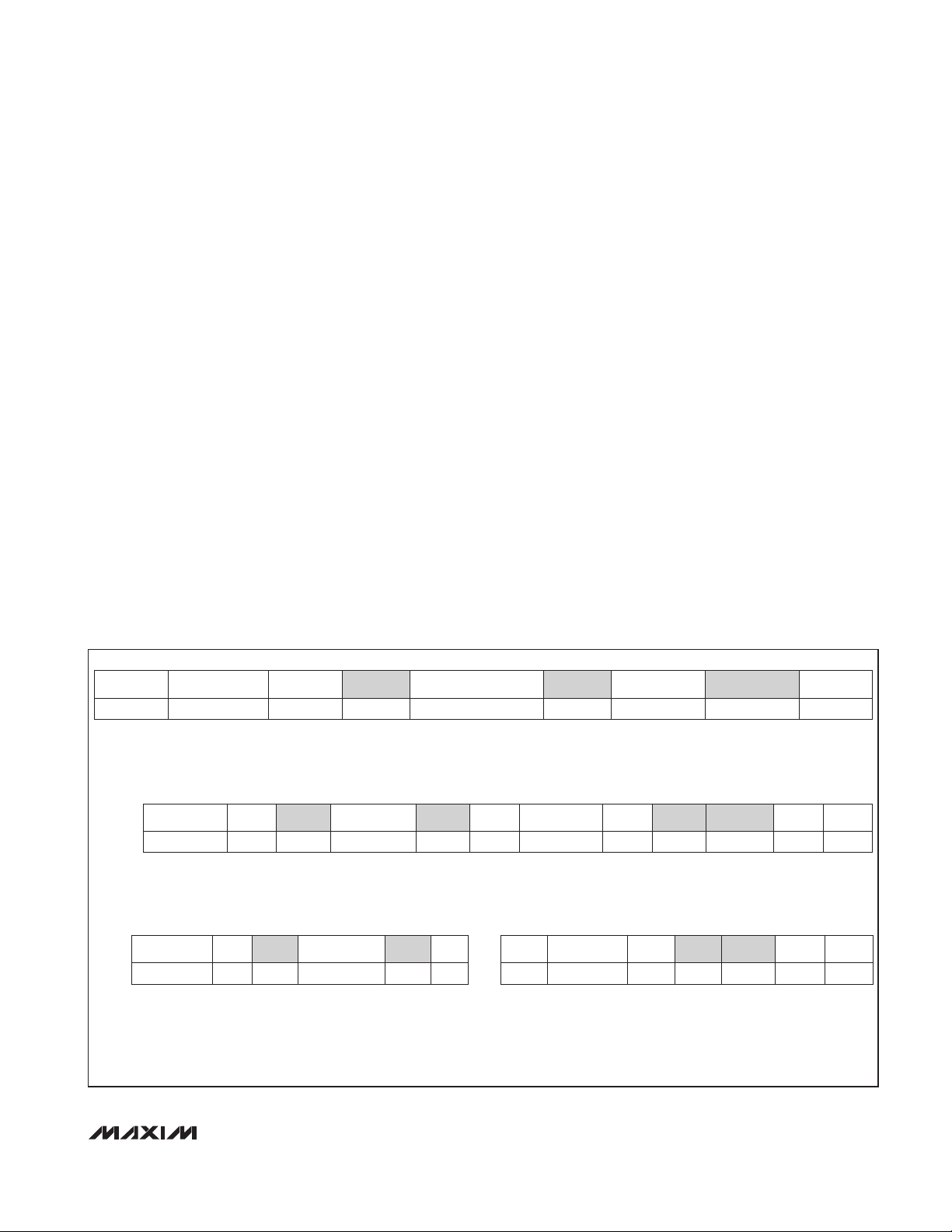
The MAX6657/MAX6658/MAX6659 employ four standard SMBus protocols: Write Byte, Read Byte, Send
Byte, and Receive Byte (Figures 2, 3, and 4). The shorter Receive Byte protocol allows quicker transfers, provided that the correct data register was previously
selected by a Read Byte instruction. Use caution with
the shorter protocols in multimaster systems, since a
second master could overwrite the command byte without informing the first master.
When the conversion rate is greater than 4Hz, temperature
data can be read from the Read Internal Temperature
(00h) and Read External Temperature (01h) registers.
The temperature data format is 7 bits + sign in two'scomplement form for each channel, with the LSB representing 1°C (Table 2). The MSB is transmitted first.
When the conversion rate is 4Hz or less, the first 8 bits
of temperature data can be read from the Read Internal
Temperature (00h) and Read External Temperature
(01h) registers, the same as for faster conversion rates.
An additional 3 bits can be read from the Read External
Extended Temperature (10h) and Read Internal
Extended Temperature (11h) registers, which extends
the data to 10 bits + sign and the resolution to
+0.125°C per LSB (Table 3).
When a conversion is complete, the Main register and
the Extended register are updated almost simultaneously. Ensure that no conversions are completed
between reading the Main and Extended registers so
that when data that is read, both registers contain the
result of the same conversion.
To ensure valid extended data, read extended resolution temperature data using one of the following
approaches:
1) Put the MAX6657/MAX6658/MAX6659 into standby
mode by setting bit 6 of the Configuration register to
MAX6657/MAX6658/MAX6659
______________________________________________________________________________________ 9
Figure 2. SMBus Protocols
ACK
7 bits
ADDRESS ACKWR
8 bits
DATA ACK
1
P
8 bits
S COMMAND
Write Byte Format
Read Byte Format
Send Byte Format Receive Byte Format
Slave Address: equivalent to chip-select line of
a 3-wire interface
Command Byte: selects which
register you are writing to
Data Byte: data goes into the register
set by the command byte (to set
thresholds, configuration masks, and
sampling rate)
ACK
7 bits
ADDRESS ACKWR S ACK
8 bits
DATA
7 bits
ADDRESS RD
8 bits
/// PCOMMAND
Slave Address: equivalent to chip-select line
Command Byte: selects
which register you are
reading from
Slave Address: repeated
due to change in dataflow direction
Data Byte: reads from
the register set by the
command byte
ACK
7 bits
ADDRESS WR
8 bits
COMMAND ACK P ACK
7 bits
ADDRESS RD
8 bits
DATA /// PS
Command Byte: sends command with no data, usually
used for one-shot command
Data Byte: reads data from
the register commanded
by the last Read Byte or
Write Byte transmission;
also used for SMBus Alert
Response return address
S = Start condition Shaded = Slave transmission
P = Stop condition /// = Not acknowledged
±1°C, SMBus-Compatible Remote/Local Temperature
Sensors with Overtemperature Alarms
MAX6657/MAX6658/MAX6659
1. Initiate a one-shot conversion using Command
Byte 0Fh. When this conversion is complete, read
the contents of the Temperature Data registers.
2) If the MAX6657/MAX6658/MAX6659 are in run mode,
read the Status register. If a conversion is in
progress, the BUSY bit is set to 1. Wait for the conversion to complete as indicated by the BUSY bit
being set to 0, then read the Temperature Data registers. Note that the power-on reset sets the conversion rate to 16Hz, so no extended data is valid
without reducing the conversion rate to 4Hz or less.
Diode Fault Alarm
There is a continuity fault detector at DXP that detects
an open circuit between DXP and DXN, or a DXP short
to VCC, GND, or DXN. If an open or short circuit exists,
the external temperature register is loaded with 1000
0000. Additionally, if the fault is an open circuit, bit 2
(OPEN) of the status byte is set to 1 and the ALERT condition is activated at the end of the conversion.
Immediately after POR, the Status register indicates that
no fault is present until the end of the first conversion.
10 ______________________________________________________________________________________
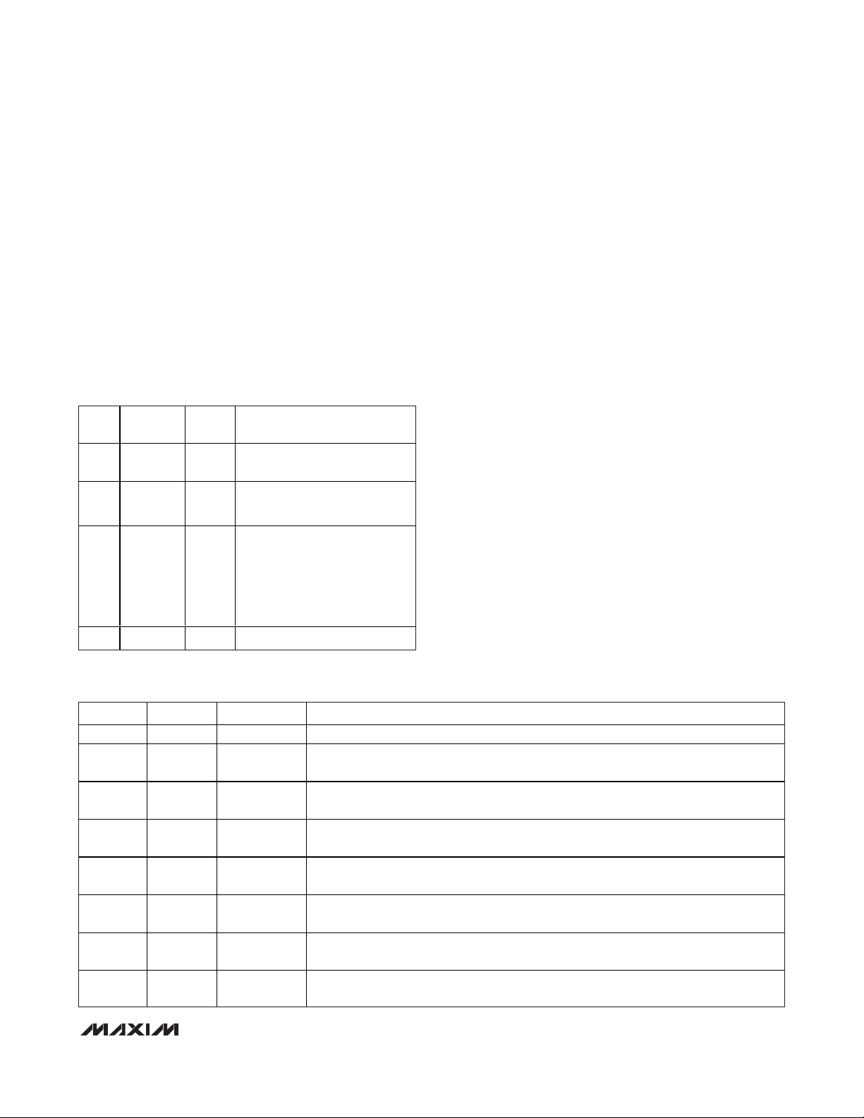
Figure 4. SMBus Read Timing Diagram
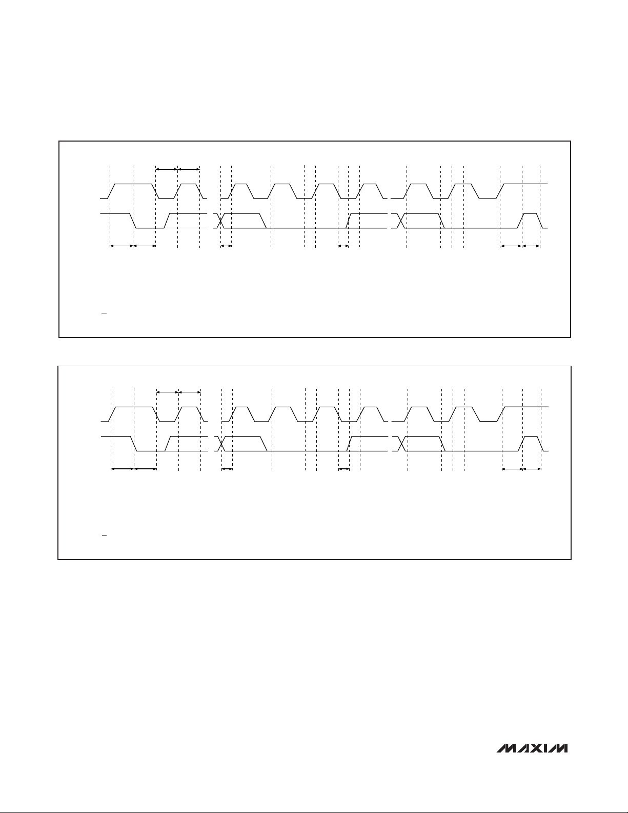
Figure 3. SMBus Write Timing Diagram
±1°C, SMBus-Compatible Remote/Local Temperature
Sensors with Overtemperature Alarms
AB CDEFG HIJ
t
LOWtHIGH
SMBCLK
SMBDATA
t
t
HD:STA
SU:STA
A = START CONDITION
B = MSB OF ADDRESS CLOCKED INTO SLAVE
C = LSB OF ADDRESS CLOCKED INTO SLAVE
D = R/W BIT CLOCKED INTO SLAVE
E = SLAVE PULLS SMBDATA LINE LOW
t
SU:DAT
F = ACKNOWLEDGE BIT CLOCKED INTO MASTER
G = MSB OF DATA CLOCKED INTO SLAVE
H = LSB OF DATA CLOCKED INTO SLAVE
I = MASTER PULLS DATA LINE LOW
t
HD:DAT
AB CDEFG HIJ
t
LOWtHIGH
SMBCLK
SMBDATA
t
SU:STA
t
HD:STA
t
SU:DAT
t
HD:DAT
K
t
SU:STO
J = ACKNOWLEDGE CLOCKED INTO SLAVE
K = ACKNOWLEDGE CLOCK PULSE
L = STOP CONDITION
M = NEW START CONDITION
K
t
SU:STO
M
L
t
BUF
M
L
t
BUF
A = START CONDITION
B = MSB OF ADDRESS CLOCKED INTO SLAVE
C = LSB OF ADDRESS CLOCKED INTO SLAVE
D = R/W BIT CLOCKED INTO SLAVE
E = SLAVE PULLS SMBDATA LINE LOW
F = ACKNOWLEDGE BIT CLOCKED INTO MASTER
G = MSB OF DATA CLOCKED INTO MASTER
H = LSB OF DATA CLOCKED INTO MASTER
I = MASTER PULLS DATA LINE LOW
J = ACKNOWLEDGE CLOCKED INTO SLAVE
K = ACKNOWLEDGE CLOCK PULSE
L = STOP CONDITION
M = NEW START CONDITION

Alarm Threshold Registers
Four registers store ALERT threshold values—one hightemperature (T
HIGH
) and one low-temperature (T
LOW
)
register each for the local and remote channels. If
either measured temperature equals or exceeds the
corresponding ALERT threshold value, the ALERT output is asserted.
The POR state of both ALERT T
HIGH
registers is 0100
0110 or +70°C and the POR state of T
LOW
registers is
1100 1001 or -55°C.
Four additional registers store remote and local alarm
threshold data corresponding to the OVERT1 and
OVERT2 (MAX6659 only) outputs. The values stored in
these registers are high-temperature thresholds. If any
one of the measured temperatures equals or exceeds
the corresponding alarm threshold value, an OVERT
output is asserted. The POR state of the OVERT threshold is 0101 0101 or +85°C.
Alert
Interrupts
An ALERT interrupt occurs when the internal or external
temperature reading exceeds a high or low temperature limit (user programmed) or when the remote diode
is disconnected (for continuity fault detection). The
ALERT interrupt output signal is latched and can be
cleared only by either reading the Status register or by
successfully responding to an Alert Response address.
In both cases, the alert is cleared even if the fault condition still exists, but is reasserted at the end of the next
conversion. The interrupt does not halt automatic conversions. The interrupt output pin is open-drain so that
multiple devices can share a common interrupt line.
The interrupt rate never exceeds the conversion rate.
Alert Response Address
The SMBus Alert Response interrupt pointer provides
quick fault identification for simple slave devices that
lack the complex, expensive logic needed to be a bus
master. Upon receiving an ALERT interrupt signal, the
host master can broadcast a Receive Byte transmission
to the Alert Response slave address (0001100). Then,
any slave device that generated an interrupt attempts
to identify itself by putting its own address on the bus
(Table 8).
The Alert Response can activate several different slave
devices simultaneously, similar to the I2C General Call.
If more than one slave attempts to respond, bus arbitration rules apply, and the device with the lower address
code wins. The losing device does not generate an
acknowledge and continues to hold the ALERT line low
until cleared. (The conditions for clearing an alert vary,
depending on the type of slave device.) Successful
completion of the Alert Response protocol clears the
interrupt latch, provided the condition that caused the
alert no longer exists. If the condition still exists, the
device reasserts the ALERT interrupt at the end of the
next conversion.
OVERT
Overtemperature
Alarm/Warning Outputs
OVERT1 and OVERT2 (MAX6659 only) are asserted
when the temperature rises to a value programmed in
the appropriate threshold register. They are deasserted
when the temperature drops below this threshold minus
the hysteresis. An OVERT output can be used to activate a cooling fan, send a warning, or trigger a system
shutdown to prevent component damage. The HYST
byte sets the amount of hysteresis for both OVERT outputs. The data format for the HYST byte is the same for
the other temperature registers (Table 2).
MAX6657/MAX6658/MAX6659
______________________________________________________________________________________ 11
Table 3. Extended Resolution Register
Note: Extended resolution applies only for conversion rates of
4Hz and slower.
Table 2. Data Format (Two's Complement)
±1°C, SMBus-Compatible Remote/Local Temperature
Sensors with Overtemperature Alarms
DIGITAL OUTPUT
TEMP (°C)
130.00 0 111 1111 0 111 1111
127.00 0 111 1111 0 111 1111
126.00 0 111 1111 0 111 1111
25 0 001 1001 0 001 1001
0.00 0 000 0000 0 000 0000
-1 1 000 0000 1 111 1111
-25 1 000 0000 1 110 0111
-55 1 000 0000 1 100 1001
Diode Fault
(Short or Open)
MAX6657
1 000 0000 1 000 0000
MAX6658
MAX6659
FRACTIONAL
TEMPERATURE
0.000 000X XXXX
0.125 001X XXXX
0.250 010X XXXX
0.375 011X XXXX
0.500 100X XXXX
0.625 101X XXXX
0.750 110X XXXX
0.875 111X XXXX
CONTENTS OF
EXTENDED REGISTER

MAX6657/MAX6658/MAX6659
For example, OVERT1 has a threshold set to +50°C
and is connected to a fan. OVERT2 has a threshold of
+75°C and is connected to a system shutdown. If the
system reaches +50°C, the fan turns on, trying to cool
the system. If the system continues to heat up to the
critical temperature of +75°C, OVERT2 causes the system to shut down.
Command Byte Functions
The 8-bit Command Byte register (Table 4) is the master
index that points to the various other registers within the
MAX6657/MAX6658/MAX6659. This register’s POR state
is 0000 0000, so a Receive Byte transmission (a protocol
that lacks the command byte) occurring immediately
after POR returns the current local temperature data.
One-Shot
The one-shot command immediately forces a new conversion cycle to begin. If the one-shot command is
received when the MAX6657/MAX6658/MAX6659 are in
software standby mode (RUN/STOP bit = 1), a new
conversion is begun, after which the device returns to
standby mode. If a conversion is in progress when a
one-shot command is received, the command is
ignored. If a one-shot command is received in autoconvert mode (RUN/STOP bit = 0) between conversions, a
new conversion begins, the conversion rate timer is
reset, and the next automatic conversion takes place
after a full delay elapses.
Configuration Byte Functions
The Configuration Byte register (Table 5) is a Read-Write
register with several functions. Bit 7 is used to mask (disable) interrupts. Bit 6 puts the device into software standby mode (STOP) or autonomous (RUN) mode. Bit 5
selects the type of external junction (set to 1 for a substrate PNP on an IC or set to 0 for a discrete diode-connected transistor) for optimized measurements. Bits 0 to
4 are reserved and return a zero when read.
12 ______________________________________________________________________________________
Table 4. Command Byte Register Assignments
±1°C, SMBus-Compatible Remote/Local Temperature
Sensors with Overtemperature Alarms
REGISTER ADDRESS POR STATE FUNCTION
RLTS 00h 0000 0000 Read Internal Temperature
RRTE 01h 0000 0000 Read External Temperature
RSL 02h 1000 0000 Read Status Register
RCL 03h 0010 0000 Read Configuration Byte
RCRA 04h 0000 1000 Read Conversion Rate Byte
RLHN 05h 0100 0110 Read Internal High Limit
RLLI 06h 1100 1001 Read Internal Low Limit
RRHI 07h 0100 0110 Read External High Limit
RRLS 08h 1100 1001 Read External Low Limit
WCA 09h 0010 0000 Write Configuration Byte
WCRW 0Ah 0000 1000 Write Conversion Rate Byte
WLHO 0Bh 0100 0110 Write Internal High Limit
WLLM 0Ch 1100 1001 Write Internal Low Limit
WRHA 0Dh 0100 0110 Write External High Limit
WRLN 0Eh 1100 1001 Write External Low Limit
OSHT 0Fh N/A One Shot
REET 10h 0000 0000 Read External Extended Temperature
RIET 11h 0000 0000 Read Internal Extended Temperature
RWO2E 16h 0101 0101 Read/Write External OVERT2 Limit (MAX6659 only)
RW02I 17h 0101 0101 Read/Write Internal OVERT2 Limit (MAX6659 only)
RWOE 19h 0101 0101 Read/Write External OVERT1 Limit
RWOI 20h 0101 0101 Read/Write Internal OVERT1 Limit
HYST 21h 0000 1010 Overtemperature Hysteresis
— FEh 4Dh Read Manufacture ID
MAX6657/MAX6658/MAX6659
______________________________________________________________________________________ 13
Status Byte Functions
The status byte (Table 6) indicates which (if any) temperature thresholds have been exceeded. This byte also
indicates whether the ADC is converting and if there is
an open-circuit fault detected with the external sense
junction. After POR, the normal state of the MSB is 1 and
all the other flag bits are 0, assuming no alert or
overtemperature conditions are present. Bits 2 through
6 of the Status register are cleared by any successful
read of the Status register, unless the fault persists. The
ALERT output follows the status flag bit. Both are
cleared when successfully read, but if the condition still
exists, they reassert at the end of the next conversion.
The bits indicating OVERT1 (bits 0 and 1) are cleared
only when the condition no longer exists. Reading the
status byte does not clear the OVERT1 outputs or fault
bits. One way to eliminate the fault condition is for the
measured temperature to drop below the temperature
threshold minus the hysteresis value. Another way to
eliminate the fault condition is by writing new values for
the OVERT1 threshold or hysteresis so that a fault condition is no longer present. Note that the status byte
does not provide status of OVERT2.
The MAX6657/MAX6658/MAX6659 incorporate collision
avoidance so that completely asynchronous operation
is allowed between SMBus operations and temperature
conversions.
When autoconverting, if the T
HIGH
and T
LOW
limits are
close together, it’s possible for both high-temp and lowtemp status bits to be set, depending on the amount of
time between status read operations. In these circumstances, it is best not to rely on the status bits to indicate reversals in long-term temperature changes.
Instead, use a current temperature reading to establish
the trend direction.
Conversion Rate Byte
The Conversion Rate register (Table 7) programs the
time interval between conversions in free-running
autonomous mode (RUN/STOP = 0). This variable rate
Table 5. Configuration-Byte Bit
Assignments
Table 6. Status Register Bit Assignments
±1°C, SMBus-Compatible Remote/Local Temperature
Sensors with Overtemperature Alarms
BIT NAME
7
(MSB)
4 to 0 RFU 0 Reserved
MASK1 0 Masks ALERT interrupts if a 1.
6 RUN/STOP 0
5 SPNP 1
POR
STATE
FUNCTION
Standby mode control bit; if a
1, standby mode is initiated.
Set to 1 when the remote
sensor is a substrate or
common collector PNP. Set to 0
when the remote sensor is a
diode-connected discrete
transistor.
BIT NAME POR STATE FUNCTION
7 (MSB) BUSY 1 A/D is busy converting when high.
6 LHIGH 0
5 LLOW 0
4 RHIGH 0
3 RLOW 0
2 OPEN 0
1 EOT1 0
0 IOT1 0
Internal high-temperature alarm has tripped when high; cleared by POR or readout of
the Status register if the fault condition no longer exists.
Internal low-temperature alarm has tripped when high; cleared by POR or readout of
the Status register if the fault condition no longer exists.
External high-temperature alarm has tripped when high; cleared by POR or readout of
the Status register if the fault condition no longer exists.
External low-temperature alarm has tripped when high; cleared by POR or readout of
the Status register if the fault condition no longer exists.
A high indicates an external diode open; cleared by POR or readout of the Status
register if the fault condition no longer exists.
A high indicates the external junction temperature exceeds the external OVERT1
threshold.
A high indicates the internal junction temperature exceeds the internal OVERT1
threshold.

MAX6657/MAX6658/MAX6659
control can be used to reduce the supply current in
portable-equipment applications. The conversion rate
byte’s POR state is 08h (16Hz). The MAX6657/
MAX6658/MAX6659 use only the 4 least-significant bits
(LSBs) of this register. The 4 most-significant bits
(MSBs) are “don’t care” and should be set to zero when
possible. The conversion rate tolerance is ±25% at any
rate setting.
Valid A/D conversion results for both channels are
available one total conversion time (125ms nominal,
156ms maximum) after initiating a conversion, whether
conversion is initiated through the RUN/STOP bit, hardware STBY pin, one-shot command, or initial power-up.
Slave Addresses
The MAX6657/MAX6658 have a fixed address of
1001100. The MAX6659 can be programmed to have
one of three different addresses, allowing up to three
devices to reside on the same bus without address
conflicts. Table 8 lists address information.
The address pin state is checked at POR only, and the
address data stays latched to reduce quiescent supply
current due to the bias current needed for high-Z state
detection.
The MAX6657/MAX6658/MAX6659 also respond to the
SMBus Alert Response slave address (see
Alert
Response Address
section).
POR and UVLO
The MAX6657/MAX6658/MAX6659 have a volatile
memory. To prevent unreliable power-supply conditions
from corrupting the data in memory and causing erratic
behavior, a POR voltage detector monitors V
CC
and
clears the memory if V
CC
falls below 1.7V (typ, see
Electrical Characteristics
). When power is first applied
and VCCrises above 2.0V (typ), the logic blocks begin
operating, although reads and writes at V
CC
levels
below 3.0V are not recommended. A second VCCcomparator and the ADC undervoltage lockout (UVLO)
comparator prevent the ADC from converting until there
is sufficient headroom (VCC= +2.8V typ).
Power-Up Defaults
Power-up defaults include:
• ADC begins autoconverting at a 16Hz rate (legacy
resolution).
• THIGH and TLOW registers are set to default limits,
respectively.
• Interrupt latch is cleared.
• Address-select pin is sampled (MAX6659 only).
• Command register is set to 00h to facilitate quick
internal Receive Byte queries.
• Hysteresis is set to 10°C.
• Transistor type is set to a substrate or common col-
lector PNP.
14 ______________________________________________________________________________________
Table 8. Slave Address Decoding for
MAX6659
Note: Extended resolution applies only for conversion rates of
4Hz or slower.
Table 7. Conversion-Rate
Control Byte
Table 9. Read Format for Alert Response
Address (000 1100)
±1°C, SMBus-Compatible Remote/Local Temperature
Sensors with Overtemperature Alarms
DATA CONVERSION RATE (Hz)
00h 0.0625
01h 0.125
02h 0.25
03h 0.5
04h 1
05h 2
06h 4
07h 8
08h 16
09h 16
0Ah-FFh Reserved
ADD CONNECTION ADDRESS
BIT NAME FUNCTION
7 (MSB) ADD7
6 ADD6
5 ADD5
4 ADD4
3 ADD3
2 ADD2
1 ADD1
0 (LSB) 1 Logic 1
GND 1001100
V
CC
Unconnected 1001101
1001110
Provide the current
MAX6659 slave address
that was latched at POR
(Table 8)

MAX6657/MAX6658/MAX6659
______________________________________________________________________________________ 15
Chip Information
PROCESS: BiCMOS
V
CC
SMBDATA
SMBCLK
DATA
CLOCK
INTERRUPTED TO µP
TO FAN DRIVER
() ARE MAX6659 ONLY
TO SYSTEM SHUTDOWN
(ADD) GND
µP
3.3V
200Ω
2200pF
10kΩ
EACH
0.1µF
DXP
DXN
ALERT
OVERT1
(OVERT2)
(STBY)
MAX6657
MAX6658
MAX6659
Typical Operating Circuit
±1°C, SMBus-Compatible Remote/Local Temperature
Sensors with Overtemperature Alarms
Package Information
For the latest package outline information and land patterns, go
to www.maxim-ic.com/packages
. Note that a “+”, “#”, or “-” in
the package code indicates RoHS status only. Package drawings may show a different suffix character, but the drawing pertains to the package regardless of RoHS status.
PACKAGE
TYPE
PACKAGE
CODE
OUTLINE NO.
LAND
PATTERN NO.
8 SO S8-5
21-0041
90-0096
16 QSOP E16-5
21-0055
90-0167
Ordering Information (continued)
Note: All devices are specified over the -55°C to +125°C operating temperature range.
+
Denotes a lead(Pb)-free/RoHS-compliant package.
T = Tape and reel.
PART
MAX6658MSA -55°C to +125°C 8 SO
MAX6658MSA+ -55°C to +125°C 8 SO
MAX6658MSA-T -55°C to +125°C 8 SO
MAX6658MSA+T -55°C to +125°C 8 SO
MAX6659MEE -55°C to +125°C 16 QSOP
MAX6659MEE+ -55°C to +125°C 16 QSOP
MAX6659MEE-T -55°C to +125°C 16 QSOP
MAX6659MEE+T -55°C to +125°C 16 QSOP
MEASURED TEMP
RANGE
PIN-PACKAGE

MAX6657/MAX6658/MAX6659
1°C Remote/Local Temperature Sensors with SMBus
Serial Interface and Overtemperature Alarms
Maxim cannot assume responsibility for use of any circuitry other than circuitry entirely embodied in a Maxim product. No circuit patent licenses are
implied. Maxim reserves the right to change the circuitry and specifications without notice at any time.
16
____________________Maxim Integrated Products, 120 San Gabriel Drive, Sunnyvale, CA 94086 408-737-7600
© 2010 Maxim Integrated Products Maxim is a registered trademark of Maxim Integrated Products, Inc.
Revision History
REVISION
NUMBER
5 10/10
REVISION
DATE
DESCRIPTION
Updated the Ordering Information table to include lead(Pb)-free parts, added the
soldering temperature to the Absolute Maximum Ratings section, replaced the
package outline drawings with the Package Information table
PAGES
CHANGED
1, 2, 15
 Loading...