

Page 1
General Description
The MAX6640 monitors its own temperature and one
external diode-connected transistor or the temperatures
of two external diode-connected transistors, typically
available in CPUs, FPGAs, or GPUs. The 2-wire serial
interface accepts standard System Management Bus
(SMBusTM) write byte, read byte, send byte, and
receive byte commands to read the temperature data
and program the alarm thresholds. Temperature data
can be read at any time over the SMBus, and three programmable alarm outputs can be used to generate
interrupts, throttle signals, or overtemperature shutdown signals.
The temperature data is also used by the internal dual
PWM fan-speed controller to adjust the speed of up to
two cooling fans, thereby minimizing noise when the
system is running cool, but providing maximum cooling
when power dissipation increases. Speed control is
accomplished by tachometer feedback from the fan, so
that the speed of the fan is controlled, not just the PWM
duty cycle. Accuracy of speed measurement is ±4%.
The MAX6640 is available in 16-pin QSOP and 16-pin
TQFN 5mm x 5mm packages. It operates from 3.0V to
3.6V and consumes just 500μA of supply current.
Applications
Desktop Computers
Notebook Computers
Workstations
Servers
Networking Equipment
Features
♦ Two Thermal-Diode Inputs
♦ Local Temperature Sensor
♦ 1°C Remote Temperature Accuracy (+60°C to
+100°C)
♦ Two PWM Outputs for Fan Drive (Open Drain; can
be Pulled Up to +13.5V)
♦ Programmable Fan-Control Characteristics
♦ Automatic Fan Spin-Up Ensures Fan Start
♦ Controlled Rate-of-Change Ensures Unobtrusive
Fan-Speed Adjustments
♦ ±4% Fan-Speed Measurement Accuracy
♦ Temperature Monitoring Begins at POR for Fail-
Safe System Protection
♦ OT and THERM Outputs for Throttling or
Shutdown
♦ Measures Temperatures Up to +150°C
♦ Tiny 5mm x 5mm 16-Pin TQFN and QSOP
Packages
MAX6640
2-Channel Temperature Monitor with Dual
Automatic PWM Fan-Speed Controller
________________________________________________________________
Maxim Integrated Products
1
Ordering Information
19-3344; Rev 2; 10/08
For pricing, delivery, and ordering information, please contact Maxim Direct at 1-888-629-4642,
or visit Maxim’s website at www.maxim-ic.com.
EVALUATION KIT
AVAILABLE
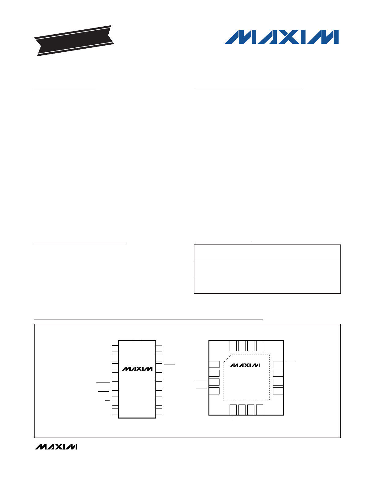
Pin Configurations
SMBus is a trademark of Intel Corp.
Typical Operating Circuit appears at end of data sheet.
+
Denotes a lead-free/RoHS-compliant package.
*
EP = Exposed pad.
PART
M AX6640AE E +
M AX6640ATE +
O PER A T IN G
R A NG E
-40°C to
+125°C
-40°C to
+125°C
M EA SU R EM EN T
R A N G E
0°C to +150°C 16 QSOP
0°C to +150°C 16 TQFN- EP*
PINPACKAGE
PWM1
SDA
TOP VIEW
PWM1
TACH1
PWM2
TACH2
FANFAIL
THERM
V
+
1
2
3
MAX6640
4
5
6
OT
7
8
CC
QSOP
16
SCL
15
SDA
ALERT
14
13
I.C.
12
DXP2
DXN
11
10
GND
9
DXP1
PWM2 1
TACH2 2
FANFAIL
THERM
+
3
4
TACH1
16
15 14 13
MAX6640
*CONNECT EXPOSED
PAD TO GND
6 7 8
5
OT
5mm x 5mm THIN QFN
SCL
12
ALERT
I.C.11
109DXP2
DXN
CC
V
GND
DXP1
Page 2

MAX6640
2-Channel Temperature Monitor with Dual
Automatic PWM Fan-Speed Controller
2 _______________________________________________________________________________________
ABSOLUTE MAXIMUM RATINGS
ELECTRICAL CHARACTERISTICS
(VCC= +3.0V to +3.6V, TA= 0°C to +125°C, unless otherwise noted. Typical values are at VCC= +3.3V, TA= +85°C.) (Note 1)
Stresses beyond those listed under “Absolute Maximum Ratings” may cause permanent damage to the device. These are stress ratings only, and functional
operation of the device at these or any other conditions beyond those indicated in the operational sections of the specifications is not implied. Exposure to
absolute maximum rating conditions for extended periods may affect device reliability.
VCCto GND..............................................................-0.3V to +6V
PWM1, PWM2, TACH1, and TACH2 to GND......-0.3V to +13.5V
DXP1 and DXP2 to GND ..........................-0.3V to +(V
CC
+ 0.3V)
DXN to GND ..........................................................-0.3V to +0.8V
SCL, SDA, THERM, OT, FANFAIL,
and ALERT to GND..............................................-0.3V to +6V
SDA, OT, THERM, ALERT, FANFAIL,
PWM1, and PWM2 Current .............................-1mA to +50mA
DXN Current .......................................................................±1mA
ESD Protection (all pins, Human Body Model)..................2000V
Continuous Power Dissipation (T
A
= +70°C)
16-Pin QSOP (derated 8.3mW/°C above +70°C)....... 667mW
16-Pin TQFN 5mm x 5mm
(derated at 33.3mW/°C above +70°C)................2666.7mW
Operating Temperature Range .........................-40°C to +125°C
Junction Temperature......................................................+150°C
Storage Temperature Range .............................-65°C to +150°C
Lead Temperature (soldering, 10s) .................................+300°C
PARAMETER SYMBOL CONDITIONS MIN TYP MAX UNITS
Operating Supply Voltage Range V
Standby Current SMB static, sleep mode 3 10 μA
Operating Current Interface inactive, ADC active 0.5 1 mA
External Temperature Error
Internal Temperature Error
Supply Sensitivity of Temperature
Measurement
Temperature Resolution
Conversion Time 125 ms
Conversion-Rate Timing Error -10 +10 %
PWM Frequency Error -10 +10 %
Tachometer Accuracy
Remote-Diode Sourcing Current
DXN Source Voltage 0.7 V
CC
VCC = +3.3V, +60°C ≤ TA ≤ +100°C and
+60°C ≤ T
VCC = +3.3V, +40°C ≤ TA ≤ +100°C and
0°C ≤ T
V
CC
0°C ≤ T
VCC = +3.3V,
+25°C ≤ T
V
CC
0°C ≤ T
V
CC
+60°C ≤ T
High level 70 100 130
Low level 7.0 10 13.0
R
≤ +145°C
R
= +3.3V,
≤ +145°C
R
A
= +3.3V,
≤ +125°C
A
= 3.135V to 3.345V,
A
≤ +100°C
≤ +100°C
≤ +85°C
+3.0 +3.6 V
±0.2 °C/V
+0.125 °C
11 Bits
±1
±2.5
±3.8
±2
±4
±4 %
°C
°C
μA
Page 3

MAX6640
2-Channel Temperature Monitor with Dual
Automatic PWM Fan-Speed Controller
_______________________________________________________________________________________ 3
ELECTRICAL CHARACTERISTICS (continued)
(VCC= +3.0V to +3.6V, TA= 0°C to +125°C, unless otherwise noted. Typical values are at VCC= +3.3V, TA= +85°C.) (Note 1)
Note 1: All parameters tested at a single temperature. Specifications are guaranteed by design.
Note 2: Timing specifications guaranteed by design.
Note 3: The serial interface resets when SCL is low for more than t
TIMEOUT
.
Note 4: A transition must internally provide at least a hold time to bridge the undefined region (300ns max) of SCL's falling edge.
PARAMETER SYMBOL CONDITIONS MIN TYP MAX UNITS
DIGITAL INPUTS AND OUTPUTS
Output Low Voltage (Sink
Current) (OT, ALERT, FANFAIL,
THERM, SDA, PWM1, and PWM2)
Output High Leakage Current
(OT, ALERT, FANFAIL, THERM,
SDA, PWM1, and PWM2)
Logic-Low Input Voltage (SDA,
SCL, THERM, TACH1, TACH2)
Logic-High Input Voltage (SDA,
SCL, THERM, TACH1, TACH2)
Input Leakage Current (SDA,
SCL, THERM, TACH1, TACH2)
Input Capacitance C
SMBus TIMING (Note 2)
Serial Clock Frequency f
Clock Low Period t
Clock High Period t
Bus Free Time Between Stop and
Start Condition
SMBus Start Condition Setup
Time
Start Condition Hold Time t
Stop Condition Setup Time t
Data Setup Time t
Data Hold Time t
SMBus Fall Time t
SMBus Rise Time t
SMBus Timeout t
t
SU:STA
HD:STO
SU:STO
SU:DAT
HD:DAT
TIMEOUT
V
OL
I
OH
V
V
SCL
LOW
HIGH
t
BUF
ALERT, FANFAIL, THERM, OT
SDA I
PWM1, PWM2, I
IL
VCC = 3.3V 2.1 V
IH
V
IN
IN
(Note 3) 10 100 kHz
10% to 10% 4 μs
90% to 90% 4.7 μs
90% of SMBCLK to 90% of SMBDATA 4.7 μs
10% of SDA to 10% of SCL 4 μs
90% of SCL to 10% of SDA 4 μs
10% of SDA to 10% of SCL 250 ns
10% of SCL to 10% of SDA (Note 4) 300 ns
F
R
= 6mA
SINK
= 4mA 0.4
SINK
= VCC or GND 1 μA
5pF
4.7 μs
58 74 90 ms
0.4
1μA
0.8 V
300 ns
1000 ns
V
Page 4
MAX6640
2-Channel Temperature Monitor with Dual
Automatic PWM Fan-Speed Controller
4 _______________________________________________________________________________________
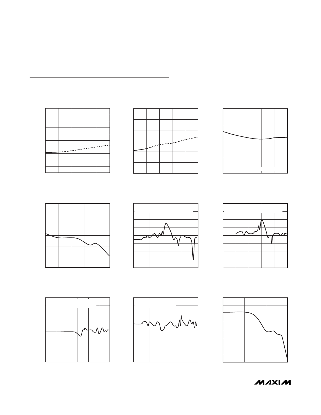
Typical Operating Characteristics
(VCC= 3.3V, TA= +25°C.)
STANDBY SUPPLY CURRENT
vs. SUPPLY VOLTAGE
MAX6640 toc01
SUPPLY VOLTAGE (V)
SUPPLY CURRENT (µA)
5.04.54.03.5
1
2
3
4
5
6
7
8
9
10
0
3.0 5.5
OPERATING SUPPLY CURRENT
vs. SUPPLY VOLTAGE
MAX6640 toc02
SUPPLY VOLTAGE (V)
SUPPLY CURRENT (µA)
5.04.54.03.5
300
400
500
600
700
800
200
3.0 5.5
REMOTE TEMPERATURE ERROR
vs. REMOTE-DIODE TEMPERATURE
MAX6640 toc03
TEMPERATURE (°C)
TEMPERATURE ERROR (°C)
100755025
-1
0
1
2
-2
0 125
FAIRCHILD 2N3906
LOCAL TEMPERATURE ERROR
vs. DIE TEMPERATURE
MAX6640 toc04
TEMPERATURE (°C)
TEMPERATURE ERROR (°C)
100755025
-0.5
-1.0
-1.5
0
0.5
1.0
-2.0
0 125
LOCAL TEMPERATURE ERROR
vs. POWER-SUPPLY NOISE FREQUENCY
MAX6640 toc06
FREQUENCY (Hz)
TEMPERATURE ERROR (°C)
10k1k100
-1.5
-1.0
-0.5
0
0.5
1.0
1.5
2.0
-2.0
1 10 100k
VIN = 250mV
P-P
SQUARE WAVE APPLIED TO
V
CC
WITH NO BYPASS CAPACITOR
REMOTE TEMPERATURE ERROR
vs. COMMON-MODE NOISE FREQUENCY
MAX6640 toc07
FREQUENCY (Hz)
TEMPERATURE ERROR (°C)
10k1k100
-1.5
-1.0
-0.5
0
0.5
1.0
1.5
2.0
-2.0
0.1 1 10 100k
VIN = AC-COUPLED TO DXP AND DXN
V
IN
= 100mV
P-P
SQUARE WAVE
REMOTE TEMPERATURE ERROR
vs. DIFFERENTIAL NOISE FREQUENCY
MAX6640 toc08
FREQUENCY (Hz)
TEMPERATURE ERROR (°C)
10k1k100
-1.5
-1.0
-0.5
0
0.5
1.0
1.5
2.0
-2.0
10 100k
VIN = AC-COUPLED TO DXP
V
IN
= 100mV
P-P
SQUARE WAVE
TEMPERATURE ERROR
vs. DXP-DXN CAPACITANCE
MAX6640 toc09
DXP-GND CAPACITANCE (nF)
TEMPERATURE ERROR (°C)
101
-5.0
-4.0
-3.0
-2.0
-1.0
0
1.0
2.0
-6.0
0.1 100
REMOTE TEMPERATURE ERROR
vs. POWER-SUPPLY NOISE FREQUENCY
MAX6640 toc05
FREQUENCY (Hz)
TEMPERATURE ERROR (°C)
10k1k100
-1.5
-1.0
-0.5
0
0.5
1.0
1.5
2.0
-2.0
10 100k
VIN = 250mV
P-P
SQUARE WAVE APPLIED TO
V
CC
WITH NO BYPASS CAPACITOR
Page 5

MAX6640
2-Channel Temperature Monitor with Dual
Automatic PWM Fan-Speed Controller
_______________________________________________________________________________________ 5
Pin Description
Typical Operating Characteristics (continued)
(VCC= 3.3V, TA= +25°C.)
PWMOUT FREQUENCY
vs. DIE TEMPERATURE
MAX6640 toc10
TEMPERATURE (°C)
PWMOUT FREQUENCY (Hz)
85603510-15
31
32
33
34
35
30
-40 110
PWMOUT FREQUENCY
vs. SUPPLY VOLTAGE
MAX6640 toc11
SUPPLY VOLTAGE (V)
PWMOUT FREQUENCY (Hz)
5.04.54.03.5
31
32
33
34
35
30
3.0 5.5
PIN
TQFN-EP QSOP
1, 15
3, 1
2, 16 4, 2
35FANFAIL Active-Low, Open-Drain, Fan-Failure Output. Open circuit when VCC = 0.
46THERM
57OT
68VCCPower-Supply Input. 3.3V nominal. Bypass VCC to GND with a 0.1μF capacitor.
7 10 GND Ground. Connect to a clean ground reference.
8, 10 9, 12
9 11 DXN
11 13 I.C. Internally Connected. Connect to VCC.
12 14 ALERT Active-Low, Open-Drain SMBus Alert Output
13 16 SCL S M Bus S er i al - C l ock Inp ut. C an b e p ul l ed up to 5.5V r eg ar d l ess of V
14 15 SDA
——EP
NAME FUNCTION
PWM2,
PWM1
TACH2,
TACH1
Open-Drain Output to Power Transistor Driving Fan. Connect to the gate of a MOSFET or base of a
bipolar transistor. PWM_ requires a pullup resistor. The pullup resistor can be connected to a
supply voltage as high as 13.5V, regardless of the MAX6640’s supply voltage.
Tachometer Inputs. Connect to the tachometer output of the fan. TACH_ requires a pullup resistor.
The pullup resistor can be connected to a supply voltage as high as 13.5V, regardless of the
MAX6640’s supply voltage.
Active-Low, Open-Drain Thermal Alarm Output. Typically used for clock throttling. Open circuit
CC
= 0.
when V
Active-Low, Open-Drain Overtemperature Output. Typically used for system shutdown or clock
DXP1,
DXP2
throttling. Can be pulled up to 5.5V regardless of V
Combined Current Source and A/D Positive Input for Remote Diode. Connect to anode of remotediode-connected temperature-sensing transistor. Do not leave unconnected; connect to DXN if no
remote diode is used. Place a 2200pF capacitor between DXP_ and DXN for noise filtering.
CC
Combined Current Sink and A/D Negative Input for Remote Diode. Connect cathode of the remotediode-connected transistor to DXN.
SMBus Serial-Data Input/Output, Open Drain. Can be pulled up to 5.5V regardless of V
circuit when V
CC
= 0.
Exposed Pad (TQFN package only). Internally connected to GND. Connect to a large ground
plane to maximize thermal performance. Not intended as an electrical connection point.
. Open circuit when VCC = 0.
. O p en ci r cui t w hen V
C C
C C
CC
= 0.
. Open
Page 6
MAX6640
Detailed Description
The MAX6640 monitors its own temperature and a
remote diode-connected transistor or the temperatures
of two external diode-connected transistors, which typically reside on the die of a CPU or other integrated circuit. The 2-wire serial interface accepts standard
SMBus write byte, read byte, send byte, and receive
byte commands to read the temperature data and program the alarm thresholds. Temperature data can be
read at any time over the SMBus, and a programmable
alarm output can be used to generate interrupts, throttle signals, or overtemperature shutdown signals.
The temperature data is also used by the internal dual
PWM fan-speed controller to adjust the speed of up to
two cooling fans, thereby minimizing noise when the
system is running cool, but providing maximum cooling
when power dissipation increases. RPM feedback
allows the MAX6640 to control the fan’s actual speed.
2-Channel Temperature Monitor with Dual
Automatic PWM Fan-Speed Controller
6 _______________________________________________________________________________________
Block Diagram
Write Byte Format
Read Byte Format
Send Byte Format
Receive Byte Format
Slave Address: equivalent to chip-select line of
a 3-wire interface
Command Byte: selects which
register you are writing to
Data Byte: data goes into the register
set by the command byte (to set
thresholds, configuration masks, and
sampling rate)
Slave Address: equivalent to chip-select line
Command Byte: selects
which register you are
reading from
Slave Address: repeated
due to change in dataflow direction
Data Byte: reads from
the register set by the
command byte
Command Byte: sends command with no data, usually
used for one-shot command
Data Byte: reads data from
the register commanded
by the last Read Byte or
Write Byte transmission;
also used for SMBus Alert
Response return address
S = Start condition Shaded = Slave transmission
P = Stop condition /// = Not acknowledged
Figure 1. SMBus Protocols
S ADDRESS RD ACK DATA /// P
7 bits 8 bits
WRS ACK COMMAND ACK P
8 bits
ADDRESS
7 bits
P
1
ACKDATA
8 bits
ACKCOMMAND
8 bits
ACKWRADDRESS
7 bits
S
S ADDRESS WR ACK COMMAND ACK S ADDRESS
7 bits8 bits7 bits
RD ACK DATA
8 bits
/// P
DXP1
DXN
DXP2
SDA
SCL
TEMPERATURE
PROCESSING
BLOCK
INTERFACE AND
REGISTERS
SMBus
V
CC
MAX6640
PWM
GENERATOR
BLOCK
LOGIC
GND
PWM1
PWM2
OT
THERM
FANFAIL
ALERT
TAC H1
TAC H2
Page 7
SMBus Digital Interface
From a software perspective, the MAX6640 appears as
a set of byte-wide registers. This device uses a standard SMBus 2-wire/I2C-compatible serial interface to
access the internal registers. The MAX6640 has a fixed
slave address of 0101111.
The MAX6640 employs four standard SMBus protocols:
write byte, read byte, send byte, and receive byte
(Figures 1, 2, and 3). The shorter receive byte protocol
allows quicker transfers, provided that the correct data
register was previously selected by a read byte instruction. Use caution with the shorter protocols in multimaster systems, since a second master could overwrite the
command byte without informing the first master.
Table 3 details the register addresses and functions,
whether they can be read or written to, and the poweron reset (POR) state. See Tables 4–8 for all other register functions and the
Register Descriptions
section.
Temperature Reading
Temperature data can be read from registers 00h and
01h. The temperature data format for these registers is
8 bits, with the LSB representing 1°C (Table 1) and the
MSB representing +128°C. The MSB is transmitted first.
Three additional temperature bits provide resolution
down to 0.125°C and are in the channel 1 extended
temperature (05h) and channel 2 extended temperature
(06h) registers. All values below 0°C clip to 00h.
The MAX6640 employs a register lock mechanism to
avoid getting temperature results from the temperature
register and the extended temperature register sampled at two different time points. Reading the extended
register stops the MAX6640 from updating the temperature register for at least 0.25s, unless there is a temperature register read before the scheduled update. This
allows enough time to read the main register before it is
MAX6640
2-Channel Temperature Monitor with Dual
Automatic PWM Fan-Speed Controller
_______________________________________________________________________________________ 7
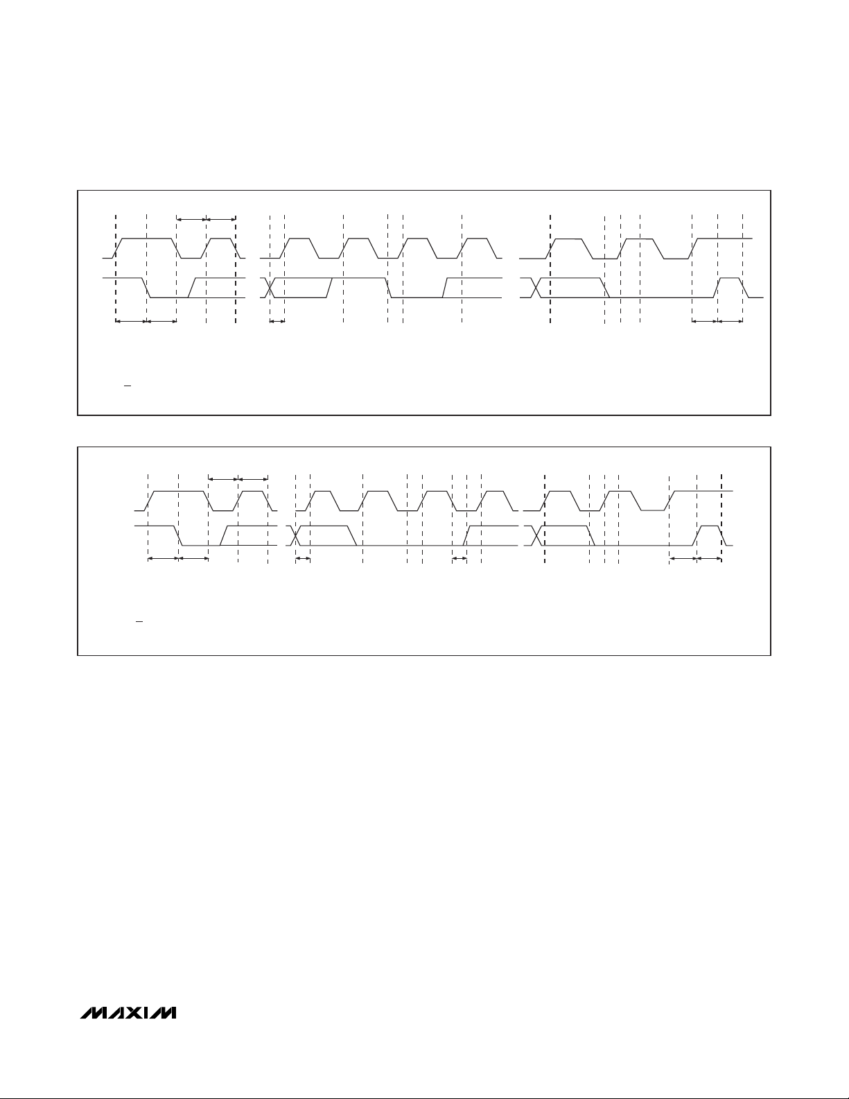
Figure 2. SMBus Write Timing Diagram
Figure 3. SMBus Read Timing Diagram
AB CDEFG
t
t
HIGH
LOW
SCL
SDA
t
SU:STAtHD:STA
A = START CONDITION
B = MSB OF ADDRESS CLOCKED INTO SLAVE
C = LSB OF ADDRESS CLOCKED INTO SLAVE
D = R/W BIT CLOCKED INTO SLAVE
t
SU:DAT
AB CDEFG HIJ
t
LOWtHIGH
SCL
SDA
t
t
HD:STA
SU:STA
A = START CONDITION
B = MSB OF ADDRESS CLOCKED INTO SLAVE
C = LSB OF ADDRESS CLOCKED INTO SLAVE
D = R/W BIT CLOCKED INTO SLAVE
E = SLAVE PULLS SMBDATA LINE LOW
E = SLAVE PULLS SMBDATA LINE LOW
F = ACKNOWLEDGE BIT CLOCKED INTO MASTER
G = MSB OF DATA CLOCKED INTO SLAVE
H = LSB OF DATA CLOCKED INTO SLAVE
t
SU:DAT
F = ACKNOWLEDGE BIT CLOCKED INTO MASTER
G = MSB OF DATA CLOCKED INTO MASTER
H = LSB OF DATA CLOCKED INTO MASTER
I = MASTER PULLS DATA LINE LOW
t
HD:DAT
HIJ
I = MASTER PULLS DATA LINE LOW
J = ACKNOWLEDGE CLOCKED INTO SLAVE
K = ACKNOWLEDGE CLOCK PULSE
L = STOP CONDITION
M = NEW START CONDITION
K
t
SU:STO
J = ACKNOWLEDGE CLOCKED INTO SLAVE
K = ACKNOWLEDGE CLOCK PULSE
L = STOP CONDITION
M = NEW START CONDITION
LMK
t
SU:STOtBUF
M
L
t
BUF
Page 8

MAX6640
updated, thereby preventing reading the temperature
register data from one conversion and the extended
temperature register data from a different conversion.
The MAX6640 measures the temperature at a fixed rate
of 4Hz immediately after it is powered on. Setting bit 7
of the configuration register (04h) shuts down the temperature measurement cycle.
OT
Output
When a measured temperature exceeds the corresponding OT temperature threshold and OT is not
masked, the associated OT status register bit sets and
the OT output asserts. If OT for the respective channel
is masked, the OT status register sets, but the OT output does not assert. To deassert the OT output and the
associated status register bit, either the measured temperature must fall at least 5°C below the trip threshold
or the trip threshold must be increased to at least 5°C
above the current measured temperature.
THERM
When a measured temperature exceeds the corresponding THERM temperature threshold and THERM is
not masked, the associated THERM status register bit
is set and the THERM output asserts. If THERM for the
respective channel is masked, the THERM status register is set, but the THERM output does not assert. To
deassert the THERM output and the associated status
register bit, either the measured temperature must fall
at least 5°C below the trip threshold or the trip threshold
must be increased to at least 5°C above the current
measured temperature. Asserting THERM internally or
externally forces both PWM outputs to 100% duty cycle
when bit 6 in address 13h (fan 1) or bit 6 in address
17h (fan 2) is set.
ALERT
The ALERT output asserts to indicate that a measured
temperature exceeds the ALERT trip threshold for that
temperature channel. The status bit and the ALERT out-
put clear by reading the ALERT status register. If the
ALERT status bit is cleared, but the temperature still
exceeds the ALERT temperature threshold, ALERT
reasserts on the next conversion, and the status bit sets
again. A successful alert response protocol clears
ALERT, but does not affect the ALERT status bit.
TACH1 and TACH2 Inputs
To measure the fan speed, the MAX6640 has two
tachometers. Each tachometer has an accurate internal
clock to count the time elapsed in one revolution.
Therefore, it is counting the time between two tachometer pulses for a fan with four poles. When the PWM signal is used to directly modulate the fan’s power supply,
the PWM frequency is normally in the 20Hz to 100Hz
range. In this case, the time required for one revolution
may be longer than the PWM on-time. For this reason,
the PWM pulses are periodically stretched to allow
tachometer measurement over a full revolution. Turn off
pulse stretching by setting bit 5 of register 13h or register 17h when using a 4-wire fan.
The tachometer count is inversely proportional to the
fan’s RPM. The tachometer count data is stored in register 20h (for TACH1) and register 21h (for TACH2).
Reading a value of 255 from the TACH count register
means the fan’s RPM is zero or too slow for the range.
Reading a value of zero in the TACH count register
means the fan’s RPM is higher than the range selected.
Table 2 shows the fan’s available RPM ranges. Use registers 10h or 14h to select the appropriate RPM range for
the fan being used.
FANFAIL
The FANFAIL output asserts to indicate that one of the
fans has failed or is spinning slower than the required
speed. The MAX6640 detects fan fault depending on
the fan control mode. In PWM mode, the MAX6640 produces a square wave with a duty cycle set by the value
written to the duty-cycle registers (26h and 27h). In this
mode, the MAX6640 signals a fan fault when the
tachometer count is greater than the maximum
tachometer count value stored in the appropriate register (22h and 23h). After the MAX6640 asserts FANFAIL,
the fan with a tachometer fault goes to full speed for 2s in
an attempt to restart the fan and then returns to the original duty-cycle settings. Reading the status register clears
2-Channel Temperature Monitor with Dual
Automatic PWM Fan-Speed Controller
8 _______________________________________________________________________________________
Table 1. Temperature Data Byte Format
FAN RPM
RANGE
INTERNAL CLOCK
FREQUENCY (kHz)
2000 1
4000 2
8000 4
16,000 8
Table 2. Tachometer Setting
TEMP (°C) TEMP (°C) DIGITAL OUTPUT
241 +241 1111 0001
240 +240 1111 0000
126 +126 0111 1110
25 +25 0001 1001
1.50 1 0000 0001
0.00 0 0000 0000
Page 9

the FANFAIL status bits and the output. The MAX6640
measures the fan speed again after 2s. The MAX6640
asserts FANFAIL if it detects the fan fault again.
In RPM mode (either automatic or manual), the
MAX6640 checks for fan failure only when the duty
cycle reaches 100%. It asserts FANFAIL when the
tachometer count is greater than twice the target
tachometer count. In manual RPM mode, registers 22h
and 23h store the target tachometer count value. In
automatic RPM mode, these registers store the maximum tachometer count.
Fan-Speed Control
The MAX6640 adjusts fan speed by controlling the duty
cycle of a PWM signal. This PWM signal then either
modulates the DC brushless fan’s power supply or drives a speed-control input on a fan that is equipped with
one. There are three speed-control modes: PWM, in
which the PWM duty cycle is directly programmed over
the SMBus; manual RPM, in which the desired
tachometer count is programmed into a register and
the MAX6640 adjusts its duty cycle to achieve the
desired tachometer count; and automatic RPM, in
which the tachometer count is adjusted based on a
programmed temperature profile.
The MAX6640 divides each PWM cycle into 120 time
slots. Registers 26h and 27h contain the current values
of the duty cycles for PWM1 and PWM2, expressed as
the effective time slot length. For example, the PWM1
output duty cycle is 25% when register 26h reads 1Eh
(30/120).
PWM Control Mode
Enter PWM mode by setting bit 7 of the fan 1 or 2 configuration 1 register (10h and 14h) to 1. In PWM control
mode, the MAX6640 generates PWM signals whose
duty cycles are specified by writing the desired values
to fan duty-cycle registers 26h and 27h. When a new
duty-cycle value is written into one of the fan duty-cycle
registers, the duty cycle changes to the new value at a
rate determined by the rate-of-change bits [6:4] in the
fan 1 or 2 configuration 1 register. The rate-of-change
of the duty cycle ranges from 000 (immediately
changes to the new programmed value) to 111
(changes by 1/120 every 4s). See Table 4 and the
Fan
1 and 2 Configuration 1 (10h and 14h)
section.
Manual RPM Control Mode
Enter manual RPM control mode by setting bits 2, 3,
and 7 of the fan 1 or 2 configuration 1 register (10h and
14h) to zero. In the manual RPM control mode, the
MAX6640 adjusts the duty cycle and measures the fan
speed. Enter the target tachometer count in register
22h for fan 1 and register 23h for fan 2. The MAX6640
compares the target tachometer count with the measured tachometer count and adjusts the duty cycle so
that the fan speed gradually approaches the target
tachometer count.
The first time manual RPM control mode is entered, the
initial PWM duty cycle is determined by the target
tachometer count:
where targetTACH is the value of the target tachometer
count in the target tach count register (22h or 23h).
If the initial duty cycle value is over 120, the duty cycle
is 100%. If spin-up is enabled (bit 7 in registers 13h
and 17h) and the fan is not already spinning, the duty
cycle first goes to 100% and then goes to the initial
duty-cycle value. Every 2s, the MAX6640 counts the
fan’s period by counting the number of pulses stored in
registers 24h and 25h. If the count is different from the
target count, the duty cycle is adjusted.
If a nonzero rate-of-change is selected, the duty cycle
changes at the specified rate until the tachometer count
is within ±5 of the target. Then the MAX6640 gets into a
locked state and updates the duty cycle every 2s.
Automatic RPM Control Mode
In the automatic RPM control mode, the MAX6640 measures temperature, sets a target tachometer count
based on the measured temperature, and then adjusts
the duty cycle so the fan spins at the desired speed.
Enter this mode by setting bit 7 of the fan 1 or 2 configuration 1 register (10h and 14h) to zero and selecting
the temperature channel that controls the fan speed
using bits 2 and 3 of the configuration register.
In both the RPM modes (automatic and manual), the
MAX6640 implements a low limit for the tachometer
counts. This limits the maximum speed of the fan by
ensuring that the fan’s tachometer count does not go
lower than the tachometer count specified by bits 5
through 0 of register 24h for fan 1 and register 25h for
fan 2. Typical values for the minimum tachometer count
are 30h to 60h. Set the value to correspond to the fullrated RPM of the fan. See Figure 4.
Figure 5 shows how the MAX6640 calculates the target
tachometer value based on the measured temperature.
At T
MIN
, the fan spins at a minimum speed value corresponding to the maximum tachometer count value
stored in register 22h or 23h. Bit 0 of register 11h (fan
1) and register 15h (fan 2) selects the behavior below
MAX6640
2-Channel Temperature Monitor with Dual
Automatic PWM Fan-Speed Controller
_______________________________________________________________________________________ 9
tetTACHarg
Initial duty cycle
−255
=
2
Page 10

MAX6640
T
MIN
. If bit 0 is equal to zero, the fan will be completely
off below T
MIN
. When the temperature is falling, it must
drop 5°C below T
MIN
before the fan turns off. If bit 0 is
set to 1, the fan does not turn off below T
MIN
, but
instead stays at the maximum tachometer count in register 22h or 23h.
When the measured temperature is higher than T
MIN
,
the MAX6640 calculates the target tachometer count
value based on two linear equations. The target
tachometer count decreases by the tach step size
value stored in bits 7 through 4 of registers 11h and
15h each time the measured temperature increases by
the temperature step size value stored in bits 2 and 3 of
registers 11h and 15h. As the measured temperature
continues to increase, a second tachometer step size
goes into effect. Bits 3 through 0 of register 12h and
16h select the number temperature/PWM steps after
which the new step size takes effect. The new step size
is selected by bits 7 to 4 of registers 12h and 16h.
Register Descriptions
Channel 1 and Channel 2 Temperature Registers
(00h and 01h)
These registers contain the results of temperature measurements. The MSB has a weight of +128°C and the
LSB +1°C. Temperature data for remote diode 1 is in
the channel 1 temperature register. Temperature data
for remote diode 2 or the local sensor (selectable by bit
4 in the global configuration register) is in the channel 2
temperature register. Three additional temperature bits
provide resolution down to 0.125°C and are in the
channel 1 extended temperature (05h) and channel 2
extended temperature (06h) registers. The channel 1
and channel 2 temperature registers do not update until
at least 250ms after the access of the associated
extended temperature registers. All values below 0°C
return 00h.
Status Register (02h)
A 1 indicates that an ALERT, THERM, OT, or fan fault has
occurred. Reading this register clears bits 7, 6, 1, and 0.
Reading the register also clears the ALERT and
FANFAIL outputs, but not the THERM and OT outputs. If
the fault is still present on the next temperature measurement cycle, any cleared bits and outputs are set again. A
successful alert response clears the values on the outputs but does not clear the status register bits. The
ALERT bits assert when the measured temperature is
higher than the respective thresholds. The THERM and
OT outputs behave like comparators with 5°C hysteresis.
Mask Register (03h)
This register masks the ALERT, OT, THERM, and
FANFAIL outputs. A 1 prevents the corresponding fail-
ures from being asserted on these outputs. The mask
bits do not affect the status register.
Global Configuration Register (04h)
The global configuration register controls the shutdown
mode, power-on reset, SMBus timeout, and temperature channel 2 source select:
• D7: Run/Standby. Normal operation is run (0).
Setting this bit to 1 suspends conversions and puts
the MAX6640 into low-power sleep mode.
• D6: Software POR. Writing a 1 resets all registers to
their default values.
2-Channel Temperature Monitor with Dual
Automatic PWM Fan-Speed Controller
10 ______________________________________________________________________________________
Figure 4. Tachometer Target Calculation
Figure 5. RPM Target Calculation
TACH
TEMPERATURE
TACH
0xFFh
MAX
T
MIN-5TMIN
TACH
A+1
T
B
TAC H
TACH
MIN
B+1
RPM
RPM
MAX
TACH
B+1
TACH
A+1
RPM
MIN
0
T
-5 T
MIN
MIN
T
B
TEMPERATURE
Page 11

MAX6640
2-Channel Temperature Monitor with Dual
Automatic PWM Fan-Speed Controller
______________________________________________________________________________________ 11
Table 3. Register Map
READ/
WRITE
REGISTER
NO.
ADDRESS
R 00h
R 01h
R 02h
R/W 03h
R/W 04h
R 05h
R 06h
R/W 08h
R/W 09h
R/W 0Ah
R/W 0Bh
R/W 0Ch
R/W 0Dh
R/W 10h
R/W 11h
POR
STATE
0000
0000
0000
0000
0000
0000
0000
0011
0011
0000
0000
0000
0000
0000
0101
0101
0101
0101
0110
1110
0110
1110
0101
0101
0101
0101
1000
0010
0000
0000
FUNCTION D7 D6 D5 D4 D3 D2 D1 D 0
Temperature
channel 1
Temperature
channel 2
Status byte
Output mask
Global
configuration
Channel 1
extended
temperature
Channel 2
extended
temperature
Channel 1
ALERT limit
Channel 2
ALERT limit
Channel 1 OT
limit
Channel 2 OT
limit
Channel 1
THERM limit
Channel 2
THERM limit
Fan 1
configuration
1
Fan 1
Configuration
2a
MSB
(+128°C)
MSB
(+128°C)
Channel 1
ALERT
Channel 1
ALERT
Run
0 = run,
1= stby
MSB
(0.5°C)
MSB
(0.5°C)
MSB——————
MSB——————
MSB——————
MSB——————
MSB——————
MSB——————
PWM
mode
RPM step-
size A
(MSB)
——————
——————
Channel 2
ALERT
Channel 2
ALERT
POR
1 = reset
Rate of
change
(MSB)
RPM step-
size A
Channel 1OTChannel 2OTChannel 1
Channel 1OTChannel 2OTChannel 1
Tem p
channel 2
sour ce:
1 = l ocal ,
0 = r em ote
2
Reserved Reserved Reserved Reserved
Reserved Reserved Reserved Reserved
Rate of
change
(LSB)
RPM step-
size A
(LSB)
—
—
SMBus
timeout
0 =
enabled,
1 =
disabled
LSB
(0.125°C)
LSB
(0.125°C)
Rate of
change
RPM step-
size A
Channel 2
THERM
THERM
Reserved Reserved Reserved Reser ved
Fan 1
channel 1
control
Temp
step-size
A (MSB)
THERM
Channel 2
THERM
Fan 1
channel 2
control
Temp
step-size
A (LSB)
Fan 1 fault
Fan 1 fault
RPM
range
select
PWM
100% duty
cycle
( 1° C )
( 1° C )
Fan 2
Fan 2
D i od e
D i od e
( 1° C )
( 1° C )
( 1° C )
( 1° C )
( 1° C )
( 1° C )
r ang e
sel ect
M i ni m um
sp eed
0 = 0%,
1= val ue
i n 22h
LS B
LS B
faul t
faul t
faul t
faul t
LS B
LS B
LS B
LS B
LS B
LS B
RP M
fan
Page 12

MAX6640
2-Channel Temperature Monitor with Dual
Automatic PWM Fan-Speed Controller
12 ______________________________________________________________________________________
Table 3. Register Map (continued)
READ/
WRITE
REGISTER
NO.
ADDRESS
R/W 12h
R/W 13h
R/W 14h
R/W 15h
R/W 16h
R/W 17h
R 20h
R 21h
R/W 22h
R/W 23h
R/W 24h
R/W 25h
R 26h
POR
STATE
0000
0000
0100
0001
1000
0010
0000
0000
0000
0000
0100
0001
1111
1111
1111
1111
1111
1111
1111
1111
0100
0000
0100
0000
0000
0000
FUNCTION D7 D6 D5 D4 D3 D2 D1 D 0
Fan 1
configuration
2b
Fan 1
configuration
3
Fan 2
configuration
1
Fan 2
configuration
2a
Fan 2
configuration
2b
Fan 2
configuration
3
Fan 1
tachometer
count
Fan 2
tachometer
count
Fan 1 max
tach count/
target tach
count
Fan 2 max
tach count/
target tach
count
Pulses per
revolution/
fan 1
minimum
tach count
Pulses per
revolution/
fan 2
minimum
tach count
Fan 1 cur r ent
d uty cycl e
RPM step-
size B
(MSB)
Spin-up
disable
PWM
mode
RPM step-
size A
(MSB)
RPM step-
size B
(MSB)
Spin-up
disable
MSB — — — — — — LS B
MSB — — — — — — LS B
MSB — — — — — — LS B
MSB — — — — — — LS B
Pulse per
revolution
(MSB)
Pulse per
revolution
(MSB)
MSB — — — — — — LS B
RPM step-
size B
THERM to
full-speed
enable
Rate of
change
(MSB)
RPM step-
size A
RPM step-
size B
THERM to
full-speed
enable
Pulse per
revolution
(LSB)
Pulse per
revolution
(LSB)
RPM step-
size B
Pulse
stretching
disable
Rate of
change
RPM step-
size A
RPM step-
size B
Pulse
stretching
disable
Fan 1 min
tach count
(MSB)
Fan 2 min
tach count
(MSB)
RPM
step-size
B (LSB)
Reserved Reserved Reserved
Rate of
change
(LSB)
RPM
step-size
A (LSB)
RPM
step-size
B (LSB)
Reserved Reserved Reserved
Fan 1 min
tach
count
Fan 2 min
tach
count
Start
step-size
B (MSB)
Fan 2
channel 1
control
Temp
step-size
A (MSB)
Start
step-size
B (MSB)
Fan 1 min
tach
count
Fan 2 min
tach
count
Start
step-size
B
Fan 2
channel 2
control
Temp
step-size
A (LSB)
Start
step-size
B
Fan 1 min
tach
count
Fan 2 min
tach
count
Start step-
size B
Fan PWM
frequency
(MSB)
RPM
range
select
PWM
100%
duty
cycle
Start step-
size B
Fan PWM
frequency
(MSB)
Fan 1 min
tach
count
Fan 2 min
tach
count
S tar t step -
si ze B ( LS B)
Fan P WM
fr eq uency
( LSB)
RP M r ang e
select
M i ni m um fan
sp eed
0 = 0%, 1=
value in 22h
S tar t step -
si ze B ( LS B)
Fan P WM
fr eq uency
( LSB)
Fan 1 mi n
tach count
( LSB)
Fan 2 mi n
tach count
( LSB)
Page 13

• D5: SMBus Timeout Disable. Writing a zero enables
SMBus timeout for prevention of bus lockup. When
the timeout function is enabled, the SMBus interface
is reset if SDA or SCL remains low for more than
74ms (typ).
• D4: Temperature Channel 2 Source. Selects either
local or remote 2 as the source for temperature channel 2 register data. Writing a zero to this bit selects
remote 2 for temperature channel 2.
Extended Temperature Registers (05h and 06h)
These registers contain the extended temperature data
from channels 1 and 2. Bits D[7:5] contain the 3 LSBs
of the temperature data. The bit values are 0.5°C,
0.25°C, and 0.125°C. When bit 0 is set to 1, a diode
fault has been detected.
Channel 1 and Channel 2 ALERT, OT, and THERM
Limits (08h Through 0Dh)
These registers contain the temperatures above which
the ALERT, THERM, and OT status bits set and outputs
assert (for the temperature channels that are not
masked). The data format is the same as that of the
channel 1 and channel 2 temperature registers: the
LSB weight is +1°C and the MSB is +128°C.
Fan 1 and 2 Configuration 1 (10h and 14h)
The following registers control the modes of operation
of the MAX6640:
• D7: PWM Mode. D7 = 1 sets the fan into manual
PWM duty-cycle control mode. Write the target duty
cycle in the fan duty-cycle register. D7 = 0 puts the
fan into RPM control mode. To set RPM manually, set
both fan-control temperature channels (bits D2 and
D3) to zero and write the desired tachometer count
into the TACH count register.
• D[6:4]: Fan Duty-Cycle Rate-of-Change. D[6:4]
sets the time between increments of the duty cycle.
Each increment is 1/120 of the duty cycle. By adjusting the rate of change, audibility of fan-speed
changes can be traded for response time. Table 4
shows the effect of D[6:4] and, for reference, the time
required for the fan speed to change from 33% to
100% duty cycle as a function of the rate-of-change
bits.
MAX6640
2-Channel Temperature Monitor with Dual
Automatic PWM Fan-Speed Controller
______________________________________________________________________________________ 13
Table 3. Register Map (continued)
READ/
WRITE
REGISTER
NO.
ADDRESS
W 26h
R 27h
W 27h
R/W 28h
R/W 29h
R 3Dh
R 3Eh
R 3Fh
POR
STATE
0011
1100
0000
0000
0011
1100
0100
000
0100
0000
0101
1000
0100
1101
0000
0000
FUNCTION D7 D6 D5 D4 D3 D2 D1 D 0
Fan 1 target
duty cycle
Fan 2 current
duty cycle
Fan 2 target
duty cycle
Channel 1
minimum
fan-start
temperature
Channel 2
minimum
fan-start
temperature
Read device
ID
Read
manufacturer
ID
Read device
revision
MSB——————LS B
MSB——————LS B
MSB——————LS B
MSB——————LS B
MSB——————LS B
01011000
01001101
00000000
Page 14

MAX6640
• D[3:2]: Temperature Channel(s) for Fan Control.
Selects the temperature channel(s) that control the
PWM output when the MAX6640 is in automatic RPM
control mode (PWM mode bit is zero). If two channels are selected, the fan goes to the higher of the
two possible speeds. If neither channel is selected,
then the fan is in manual RPM mode and the speed
is forced to the value written to the target tach count
register 22h or 23h.
• D[1:0]: RPM Range. Scales the tachometer counter
by setting the maximum (full-scale) value of the RPM
range to 2000, 4000, 8000, or 16,000. (Table 2
shows the internal clock frequency as a function of
the range.)
Fan 1 and 2 Configuration 2a (11h and 15h)
The following registers apply to the automatic RPM control mode:
• D[7:4]: Fan RPM (Tachometer) Step-Size A.
Selects the number of tachometer counts the target
value decreases for each temperature step increase
above the fan-start temperature. Value = n + 1 (1
through 16) where n is the value of D[7:4].
• D[3:2]: Temperature Step Size. Selects the temper-
ature increment for fan control. For each temperature
step increase, the target tachometer count decreases by the value selected by D[7:4] (Table 7).
• D1: PWM Output Polarity. PWM output is low at
100% duty cycle when this bit is set to zero. PWM
output is high at 100% duty cycle when this bit is set
to 1.
• D0: Minimum Speed. Selects the value of the mini-
mum fan speed (when temperature is below the fanstart temperature in the automatic RPM control
mode). Set to zero for 0% fan drive. Set to 1 to determine the minimum fan speed by the tachometer
count value in registers 22h and 23h (fan maximum
TACH).
2-Channel Temperature Monitor with Dual
Automatic PWM Fan-Speed Controller
14 ______________________________________________________________________________________
Table 4. Fan Duty-Cycle Rate-of-Change
Table 5. Fan RPM Speed
Table 6. RPM to Tachometer Count Relationship Examples
*
Tachometer count value = ((internal clock frequency x 60) / actual RPM) (selected number of pulses per revolution / actual fan pulses)
REGISTER 10h
OR 14h D[6:4]
000 0 0000 0
001 0.0625 0.06 0.06 0.06 0.05 5
010 0.125 0.13 0.12 0.12 0.15 10
011 0.25 0.25 0.26 0.24 0.25 20
100 0.5 0.5 0.5 0.51 0.5 40
101 1 1 1 0.99 1 80
110 2 2 2 1.98 2 160
111 4 4 4 3.96 4 320
NOMINAL RATE
OF CHANGE (s)
A C T U A L R A T E O F CH A N G E AT SPEC IF I C PW M FREQUENCIES
100Hz (s) 50Hz (s) 33.3Hz (s) 20Hz (s)
NOMINAL TIME FROM
33% TO 100% (s)
D[1:0] FAN MAXIMUM RPM VALUE
00 2000
01 4000
10 8000
11 16,000
MAXIMUM RPM VALUE ACTUAL RPM
2000 1000 2 2 3Ch
4000 1000 2 2 78h
4000 3000 2 2 28h
4000 3000 2 4 14h
16,000 8000 4 4 3Ch
16,000 8000 4 2 78h
SELECTED NUMBER
OF PULSES PER
REVOLUTION
ACTUAL FAN PULSES
PER REVOLUTION
TACHOMETER COUNT
VALUE*
Page 15
Fan 1 and 2 Configuration 2b (12h and 16h)
The following registers select the tachometer step sizes
and number of steps for step-size A to step-size B
slope changes (see Figure 1):
• D[7:4]: RPM (Tachometer) Step Size B. Selects
number of tachometer counts the target value
decreases for each temperature step increase after
the number of steps selected by D[3:0]. Value = n +
1 (1 through 16) where n is the value of D[7:4].
• D[3:0]: Selects the number of temperature/tachometer steps above the fan-start temperature at which
step-size B begins.
Fan 1 and Fan 2 Configuration 3 (13h and 17h)
The following registers control fan spin-up, PWM output
frequency, pulse stretching, and THERM to fan fullspeed enable:
• D7: Fan Spin-Up Disable. Set to zero to enable fan
spin-up. Whenever the fan starts up from zero drive,
it is driven with 100% duty cycle for 2s to ensure that
it starts. Set to 1 to disable the spin-up function.
• D6: THERM to Full-Speed Enable. When this bit is
1, THERM going low (either by being pulled low
externally or by the measured temperature exceeding the THERM limit) forces the fan to full speed. In
all modes, this happens at the rate determined by
the rate-of-change selection. When THERM is
deasserted (even if fan has not reached full speed),
the speed falls at the selected rate-of-change to the
target speed.
• D5: Disable Pulse Stretching. Pulse stretching is
enabled when this bit is set to zero. When modulating the fan’s power supply with the PWM signal, the
PWM pulses are periodically stretched to keep the
tachometer signal available for one full revolution.
Setting this bit to 1 disables pulse stretching. The
MAX6640 still measures the fan speed but does not
stretch the pulses for measurements, so the fan’s
power supply must not be pulse modulated.
• D[1:0]: PWM Output Frequency. These bits control
the PWM output frequency as shown in Table 8.
Fan Tach Count 1 and 2 (20h and 21h)
These registers have the latest tachometer measurement of the corresponding channel. This is inversely
proportional to the fan’s speed. The fan RPM range
should be set so this count falls in the 30 to 160 range
for normal fan operation.
Fan Start Tach Count/Target Tach Count
(22h and 23h)
D[7:0]: This sets the starting tachometer count for the
fan in automatic RPM mode. Depending on the setting
of the minimum duty-cycle bit, the tachometer count
has this value either at all temperatures below the fanstart temperature or the count is zero below the fanstart temperature and has this value when the fan-start
temperature is reached. These registers are the target
tach count when in manual RPM mode.
Fan 1 and 2 Pulses and Min RPM (24h and 25h)
D[7:6]: This sets the number of tachometer pulses per
revolution for the fan. When set properly, a 2000RPM fan
with two pulses per revolution has the same tachometer
count as a 2000RPM fan with four pulses per revolution.
Table 9 lists tachometer pulses per revolution.
D[5:0]: This sets the minimum allowable fan tachometer
count (maximum speed). This limits the maximum
speed of the fan to reduce noise at high temperatures.
For reasonable speed resolution, the fan RPM range
should be set so this value is between about 30 and 60.
If a maximum RPM limit is unnecessary, this value can
be set to the full-speed tachometer count.
Fan 1 and 2 Duty Cycle (26h and 27h)
These registers contain the present value of the PWM
duty cycle. In PWM fan-control mode, the desired (target) value of the PWM duty cycle can be written directly
into this register.
Channel 1 and Channel 2 Fan-Start Temperature
(28h and 29h)
These registers contain the temperatures at which fan
control begins (in automatic RPM mode).
MAX6640
2-Channel Temperature Monitor with Dual
Automatic PWM Fan-Speed Controller
______________________________________________________________________________________ 15
Table 7. Temperature Step Size
Table 8. Fan PWM Frequency
D[3:2]
00 1
01 2
10 4
11 8
FAN CONTROL TEMPERATURE
STEP SIZE (°C)
D[1:0] LOW FREQUENCY (Hz)
00 20
01 33.33
10 50
11 100
Page 16

MAX6640
Applications Information
Fan-Drive Circuits
A variety of fan-drive circuit configurations can be used
with the MAX6640 to control the fan’s speed. Four of
the most common are shown in Figures 6 through 10.
PWM Power-Supply Drive (High Side or Low Side)
The simplest way to control the speed of a 3-wire (supply, ground, and tachometer output) fan is to modulate
its power supply with a PWM signal. The PWM frequency is typically in the 20Hz to 40Hz range, with 33Hz
being a common value. If the frequency is too high, the
fan’s internal control circuitry does not have sufficient
time to turn on during a power-supply pulse. If the frequency is too low, the power-supply modulation
becomes more easily audible.
The PWM can take place on the high side (Figure 6) or
the low side (Figure 7) of the fan’s power supply. In
either case, if the tachometer is used, it is usually necessary to periodically stretch a PWM pulse so there is
enough time to count the tachometer pulse edges for
speed measurement. The MAX6640 allows this pulse
stretching to be enabled or disabled to match the
needs of the application.
Pulse stretching can sometimes be audible if the fan
responds quickly to changes in the drive voltage. If the
acoustic effects of pulse stretching are too noticeable,
the circuit in Figure 8 can be used to eliminate pulse
stretching while still allowing accurate tachometer feedback. The diode connects the fan to a low-voltage
power supply, which keeps the fan’s internal circuitry
powered even when the PWM drive is zero. Therefore,
the tachometer signal is always available and pulse
stretching can be turned off. Note that this approach
prevents the fan from turning completely off, so even
when the duty cycle is 0%, the fan may still spin.
Linear Fan Supply Drive
While many fans are compatible with PWM power-supply
drive, some are excessively noisy with this approach.
When this is the case, a good alternative is to control the
fan’s power-supply voltage with a variable DC power-supply circuit. The circuit in Figure 9 accepts the PWM signal
as an input, filters the PWM, and converts it to a DC voltage that then drives the fan. To minimize the size of the filter capacitor, use the highest available PWM frequency.
Pulse stretching is not necessary when using a linear fan
supply. Note that this approach is not as efficient as PWM
drive, as the fan’s power-supply current flows through the
MOSFET, which can have an appreciable voltage across
it. The total power is still less than that of a fan running
at full speed. Table 10 is a summary of fan-drive
options.
2-Channel Temperature Monitor with Dual
Automatic PWM Fan-Speed Controller
16 ______________________________________________________________________________________
Table 9. Tachometer Pulses per
Revolution
Figure 6. High-Side PWM Drive Circuit
Figure 7. Low-Side Drive Circuit
D[7:6]
00 1
01 2
10 3
11 4
TACHOMETER PULSES PER
REVOLUTION
V
CC
V
FAN
(5V OR 12V)
V
CC
V
FAN
(5V OR 12V)
3V TO 5.5V
4.7kΩ
PWM1
3V TO 5.5V
4.7kΩ
TACH1
TACH
OUTPUT
4.7kΩ
TACH1
TACH
OUTPUT
3V TO 5.5V
4.7kΩ
PWM1
Page 17

4-Wire Fans
Some fans have an additional, fourth terminal that
accepts a logic-level PWM speed-control signal as
shown in Figure 10. These fans require no external
power circuitry and combine the low noise of linear
drive with the high efficiency of PWM power-supply
drive. Higher PWM frequencies are recommended
when using 4-wire fans.
Quick-Start Guide for 8000RPM 4-Pole
(2 Pulses per Revolution) Fan in Automatic
RPM Mode Using the Circuit of Figure 7
1) Write 02h to register 11h to set the PWM output to
drive the n-channel MOSFET.
2) Write 4Bh to register 22h to set the minimum RPM to
3200.
3) Write 5Eh to register 24h to set the pulses per revolution to 2 and to set the maximum RPM speed to
8000RPM.
4) Write 19h to register 28h to set the fan-start temperature to +25°C.
5) Write 6Ah to register 10h to start automatic
RPM mode.
Remote-Diode Considerations
Temperature accuracy depends upon having a goodquality, diode-connected, small-signal transistor.
Accuracy has been experimentally verified for all the
devices listed in Table 11. The MAX6640 can also
directly measure the die temperature of CPUs and
other ICs with on-board temperature-sensing diodes.
The transistor must be a small-signal type with a relatively high forward voltage. This ensures that the input
voltage is within the A/D input voltage range. The forward voltage must be greater than 0.25V at 10μA at the
highest expected temperature. The forward voltage
must be less than 0.95V at 100μA at the lowest expected temperature. The base resistance has to be less
than 100Ω. Tight specification of forward-current gain
(+50 to +150, for example) indicates that the manufacturer has good process control and that the devices
have consistent characteristics.
MAX6640
2-Channel Temperature Monitor with Dual
Automatic PWM Fan-Speed Controller
______________________________________________________________________________________ 17
Figure 10. 4-Wire Fan with PWM Speed-Control Input
Figure 8. High-Side PWM Drive with “Keep-Alive” Supply
Figure 9. High-Side Linear Drive Circuit
V
CC
V
FAN
(12V OR 5V)
4.7kΩ
PWM1
3V TO 5.5V
4.7kΩ
TACH1
TACH
OUTPUT
5V
V
FAN
(5V OR 12V)
V
CC
100kΩ
3.3V
4.7kΩ
100kΩ
PWM1
3V TO 5V
4.7kΩ
TACH1
TACH OUTPUT
2.2μF
2N3904
33kΩ
91kΩ
TAC H
OUTPUT
10μF
V
CC
3V TO 5.5V
4.7kΩ
PWM1
3V TO 5.5V
4.7kΩ
TACH1
TACH
OUTPUT
V
FAN
(5V OR 12V)
Page 18

MAX6640
Effect of Ideality Factor
The accuracy of the remote temperature measurements
depends on the ideality factor (n) of the remote diode
(actually a transistor). The MAX6640 is optimized for n
= 1.008, which is the typical value for the Intel®
Pentium® III and the AMD Athlon® MP model 6. If a
sense transistor with a different ideality factor is used,
the output data is different. Fortunately, the difference is
predictable.
Assume a remote-diode sensor designed for a nominal
ideality factor n
NOMINAL
is used to measure the temperature of a diode with a different ideality factor, n1.
The measured temperature TMcan be corrected using:
where temperature is measured in Kelvin.
As mentioned above, the nominal ideality factor of the
MAX6640 is 1.008. As an example, assume the
MAX6640 is configured with a CPU that has an ideality
factor of 1.002. If the diode has no series resistance,
the measured data is related to the real temperature
as follows:
For a real temperature of +85°C (358.15K), the measured temperature is +82.91°C (356.02K), which is an
error of -2.13°C.
Effect of Series Resistance
Series resistance in a sense diode contributes additional errors. For nominal diode currents of 10μA and
100μA, change in the measured voltage is:
ΔVM= RS(100μA - 10μA) = 90μA x R
S
Since 1°C corresponds to 198.6μV, series resistance
contributes a temperature offset of:
Assume that the diode being measured has a series
resistance of 3Ω. The series resistance contributes an
offset of:
The effects of the ideality factor and series resistance
are additive. If the diode has an ideality factor of 1.002
and series resistance of 3Ω, the total offset can be calculated by adding error due to series resistance with
error due to ideality factor:
1.36°C - 2.13°C = -0.77°C
for a diode temperature of +85°C.
In this example, the effect of the series resistance and
the ideality factor partially cancel each other.
For best accuracy, the discrete transistor should be a
small-signal device with its collector connected to GND
and base connected to DXN. Table 11 lists examples of
discrete transistors that are appropriate for use with the
MAX6640.
2-Channel Temperature Monitor with Dual
Automatic PWM Fan-Speed Controller
18 ______________________________________________________________________________________
Table 10. Summary of Fan-Drive Options
Table 11. Remote-Sensor Transistor
Manufacturers
Intel and Pentium are registered trademarks of Intel Corp.
AMD Athlon is a registered trademark of Advanced Micro
Devices, Inc.
FIGURE DESCRIPTION PULSE STRETCHING PWM FREQUENCY PWM POLARITY
6 High-side PWM drive Yes Low Negative
7 Low-side PWM drive Yes Low Positive
8 High-side PWM drive with keep-alive supply No Low Negative
9 High-side linear supply No High Positive
10 4-wire fan with PWM speed-control input No High Positive
TT
=
M ACTUAL
⎛
⎜
n
⎝
NOMINAL
⎞
n
1
⎟
⎠
⎛
n
TT
ACTUAL M
=
NOMINAL
⎜
⎝
⎞
⎟
n
⎠
1
1 008
⎛
T
=
M
⎜
⎝
⎞
= T
(. )1 00599
M
⎟
⎠⎠
1 002..
μ
V
90
198 6
.
Ω
=
μ
V
°
C
0 453
.
°
C
Ω
°
3 0 453 1 36Ω×
C
=°..
Ω
C
Central Semiconductor (USA) CMPT3906
Rohm Semiconductor (USA) SST3906
Samsung (Korea) KST3906-TF
Siemens (Germany) SMBT3906
MANUFACTURER MODEL NO.
Page 19

The transistor must be a small-signal type with a relatively high forward voltage; otherwise, the ADC input
voltage range can be violated. The forward voltage at
the highest expected temperature must be greater than
0.25V at 10μA, and at the lowest expected temperature,
the forward voltage must be less than 0.95V at 100μA.
Large-power transistors must not be used. Also, ensure
that the base resistance is less than 100Ω. Tight specifications for forward current gain (50 < fl < 150, for
example) indicate that the manufacturer has good
process controls and that the devices have consistent
VBEcharacteristics.
ADC Noise Filtering
The integrating ADC has inherently good noise rejection, especially of low-frequency signals such as
60Hz/120Hz power-supply hum. Micropower operation
places constraints on high-frequency noise rejection.
Lay out the printed-circuit board (PCB) carefully with
proper external noise filtering for high-accuracy remote
measurements in electrically noisy environments.
Filter high-frequency electromagnetic interference
(EMI) at DXP and DXN with an external 2200pF capacitor connected between the two inputs. This capacitor
can be increased to about 3300pF (max), including
cable capacitance. A capacitance higher than 3300pF
introduces errors due to the rise time of the switchedcurrent source.
Twisted Pairs and Shielded Cables
For remote-sensor distances longer than 8in, or in particularly noisy environments, a twisted pair is recommended. Its practical length is 6ft to 12ft (typ) before
noise becomes a problem, as tested in a noisy electronics laboratory. For longer distances, the best solution is a shielded twisted pair like that used for audio
microphones. For example, Belden #8451 works well
for distances up to 100ft in a noisy environment.
Connect the twisted pair to DXP and DXN and the
shield to ground, and leave the shield’s remote end
unterminated. Excess capacitance at DXN or DXP limits
practical remote-sensor distances (see the
Typical
Operating Characteristics
).
For very long cable runs, the cable’s parasitic capacitance often provides noise filtering, so the recommended 2200pF capacitor can often be removed or reduced
in value. Cable resistance also affects remote-sensor
accuracy. A 1Ω series resistance introduces about
+1/2°C error.
PCB Layout Checklist
1) Place the MAX6640 as close as practical to the
remote diode. In a noisy environment, such as a
computer motherboard, this distance can be 4in to
8in, or more, as long as the worst noise sources
(such as CRTs, clock generators, memory buses,
and ISA/PCI buses) are avoided.
2) Do not route the DXP/DXN lines next to the deflection
coils of a CRT. Also, do not route the traces across a
fast memory bus, which can easily introduce +30°C
error, even with good filtering. Otherwise, most noise
sources are fairly benign.
3) Route the DXP and DXN traces parallel and close to
each other, away from any high-voltage traces such
as +12VDC. Avoid leakage currents from PCB contamination. A 20MΩ leakage path from DXP ground
causes approximately +1°C error.
4) Connect guard traces to GND on either side of the
DXP/DXN traces. With guard traces, placing routing
near high-voltage traces is no longer an issue.
5) Route as few vias and crossunders as possible to
minimize copper/solder thermocouple effects.
6) When introducing a thermocouple, make sure that
both the DXP and the DXN paths have matching
thermocouples. In general, PCB-induced thermocouples are not a serious problem. A copper solder
thermocouple exhibits 3μV/°C, and it takes approximately 200μV of voltage error at DXP/DXN to cause
a +1°C measurement error, so most parasitic thermocouple errors are swamped out.
7) Use wide traces. Narrow traces are more inductive
and tend to pick up radiated noise. The 10-mil widths
and spacings recommended are not absolutely necessary (as they offer only a minor improvement in
leakage and noise), but use them where practical.
8) Placing an electrically clean copper ground plane
between the DXP/DXN traces and traces carrying
high-frequency noise signals helps reduce EMI.
MAX6640
2-Channel Temperature Monitor with Dual
Automatic PWM Fan-Speed Controller
______________________________________________________________________________________ 19
Page 20

MAX6640
2-Channel Temperature Monitor with Dual
Automatic PWM Fan-Speed Controller
20 ______________________________________________________________________________________
Typical Operating Circuit
Chip Information
PROCESS: BiCMOS
Package Information
For the latest package outline information and land patterns, go
to www.maxim-ic.com/packages
.
PACKAGE TYPE PACKAGE CODE DOCUMENT NO.
16 QSOP E16-1
21-0055
16 TQFN-EP T1655-2
21-0140
CPU
3.0V TO 3.6V
DXP1
DXN
DXP2
5V
V
I.C.
CC
TACH1
PWM1
PWM2
5V
V
FAN
(5V TO 12V)
V
FAN
5V
GPU
TO CLOCK THROTTLE
TO SMBus
MASTER
3.3V TO 5.5V
3.3V TO 5.5V 3.3V TO 5.5V
SDA
SCL
ALERT
THERM
MAX6640
GND
3.3V TO 5.5V
TACH2
FANFAIL
OT
3.3V TO 5.5V
TO SYSTEM SHUTDOWN
Page 21

MAX6640
2-Channel Temperature Monitor with Dual
Automatic PWM Fan-Speed Controller
Maxim cannot assume responsibility for use of any circuitry other than circuitry entirely embodied in a Maxim product. No circuit patent licenses are
implied. Maxim reserves the right to change the circuitry and specifications without notice at any time.
Maxim Integrated Products, 120 San Gabriel Drive, Sunnyvale, CA 94086 408-737-7600 ____________________
21
© 2008 Maxim Integrated Products is a registered trademark of Maxim Integrated Products.
Revision History
REVISION
NUMBER
0 8/04 Initial release —
1 11/07
2 10/08 Added missing exposed pad (EP) description and corrected minor errors.
REVISION
DATE
REVISION DESCRIPTION
Changed operating voltage range (General Description, EC Characteristics, TOCs
01, 02, 11, and Typical Operating Circuit); various style changes; updated Package
Information
PAGES
CHANGED
1–5, 19–23
1, 5, 7, 11, 12,
16, 17, 20
 Loading...