

Page 1
General Description
The MAX6638 thermal-management sensor includes
internal (local) and external (remote) digital temperature
sensors and two independent SMBus™ serial ports. The
remote temperature accuracy is ±1.0°C, and the local
temperature accuracy is ±2°C. The MAX6638 also features extended temperature resolution data available in
0.125°C increments.
The MAX6638 provides three system alarms: channel 1
alert (ALERT1), overtemperature (OVERT1), and channel 2 alert (ALERT2) that contain programmable thresholds set independently by each of the SMBus serial
ports (SMBus1 and SMBus2). Each alert output asserts
when any of four temperature conditions is violated:
local overtemperature, remote overtemperature, local
undertemperature, or remote undertemperature. The
overtemperature signal asserts when the temperature
rises above the value in the overtemperature limit register. Use the OVERT1 output to activate a cooling fan or
trigger a system shutdown.
Each of the 2-wire serial-interface ports accepts standard System Management Bus (SMBus) write byte, read
byte, send byte, and receive byte commands independently of one another with total collision avoidance handled by the MAX6638. Each SMBus can operate its own
unique serial-data rate to access any register in the
MAX6638 for data reads or data writes. The MAX6638
manages all dual-port data register access functions
providing a seamless, conflict-free integration into a
multimaster architecture for thermal management.
The MAX6638 performs measurements autonomously,
at the programmed conversion rate, or in a single-conversion mode. Each SMBus port can set the conversion
rate with the higher conversion and update rate dominating the average power-supply current. Single-conversion requests have a maximum delay of two
conversion cycles with channel-conversion management and cycling regulated by the dual-port controller.
The MAX6638 operating temperature range is -40°C to
+125°C and measures temperatures between 0°C and
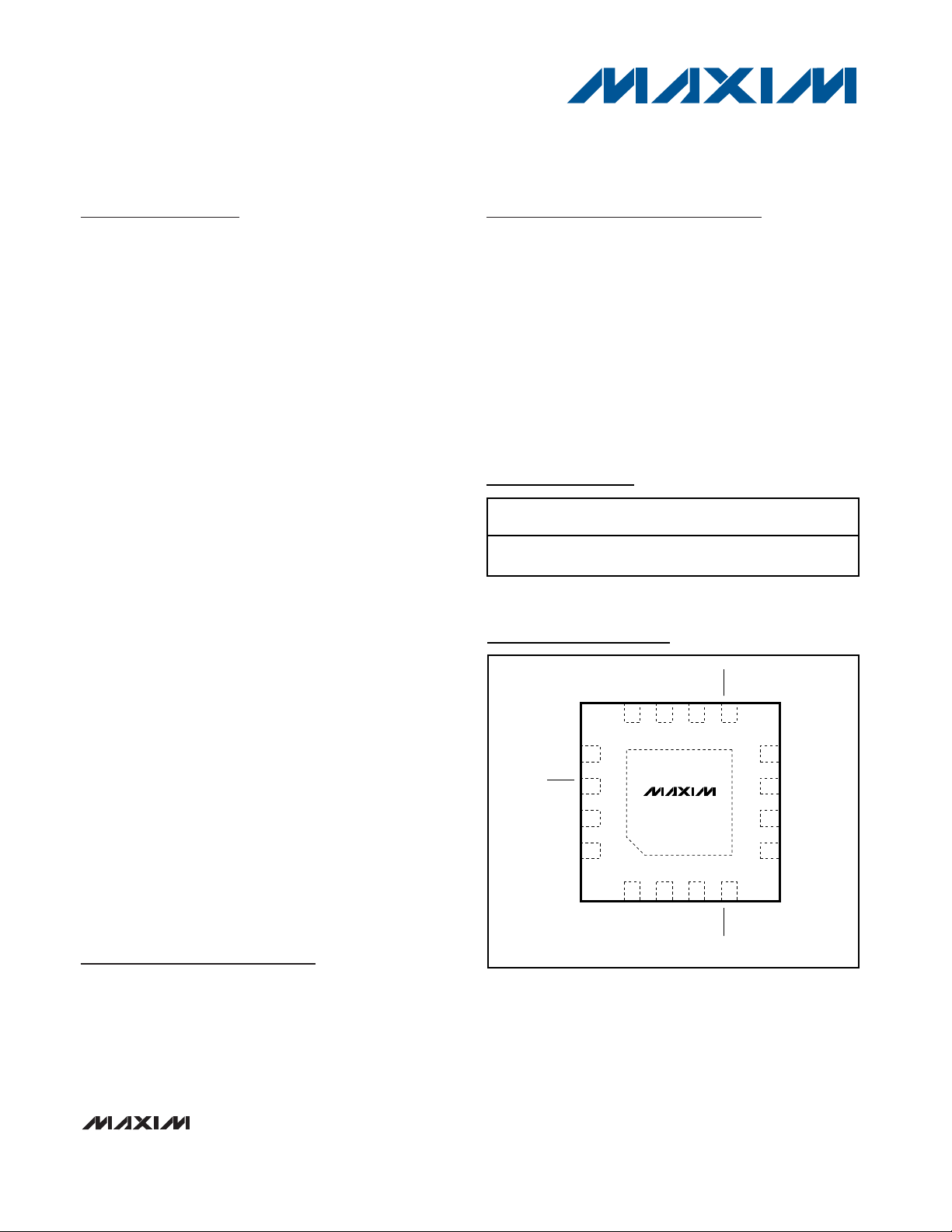
+145°C. The MAX6638 is available in a 16-pin, 4mm x
4mm TQFN with exposed paddle package.
Applications
Graphics Cards
Notebook Computers
Computer Motherboard Systems
Desktop Computers
Workstations
Features
♦ Two Independent SMBus/I2C-Compatible
Interfaces with Collision Avoidance
♦ High Accuracy
±1.0°C from +85°C to +100°C (Remote)
♦ Remote and Local Temperature Measurements
♦ Three Programmable Output Alarms: ALERT1,
OVERT1, and ALERT2
♦ Programmable Conversion Rates
♦ 11-Bit Low-Noise Integrating ADC
♦ No Calibration Required
♦ Autoscan Conversions
MAX6638
Temperature Monitor with
Dual Serial Interface
________________________________________________________________ Maxim Integrated Products 1
Ordering Information
19-3895; Rev 1; 1/06
For pricing, delivery, and ordering information, please contact Maxim/Dallas Direct! at
1-888-629-4642, or visit Maxim’s website at www.maxim-ic.com.
PART
TEMP
RANGE
PINPACKAGE
PKG
CODE
MAX6638ATE+
16 TQFN-EP*
(4mm x 4mm)
T1644-4
SMBus is a trademark of Intel Corporation.
Typical Operating Circuit appears at end of data sheet.
15
16
14
13
6
5
7
DXP
8
V
CC
SCK1
N.C.
12 4
12 11 9
SDA2
SCK2
GND
N.C.
I.C.
N.C.
MAX6638
DXN SDA1
3
10
N.C.
TQFN-EP
TOP VIEW
OVERT1 ALERT1
ALERT2
+
Pin Configuration
*EP = Exposed paddle.
+Denotes lead-free package.
-40°C to +125°C
Page 2

MAX6638
Temperature Monitor with
Dual Serial Interface
2 _______________________________________________________________________________________
ABSOLUTE MAXIMUM RATINGS
ELECTRICAL CHARACTERISTICS
(VCC= 3.0V to 5.5V, TA= -40°C to +125°C, unless otherwise noted. Typical values are at VCC= 3.3V and TA= +85°C.) (Note 1)
Stresses beyond those listed under “Absolute Maximum Ratings” may cause permanent damage to the device. These are stress ratings only, and functional
operation of the device at these or any other conditions beyond those indicated in the operational sections of the specifications is not implied. Exposure to
absolute maximum rating conditions for extended periods may affect device reliability.
(All voltages referenced to GND, unless otherwise noted.)
V
CC ....................................................................................
-0.3V to +6.0V
DXP.............................................................-0.3V to (V
CC
+ 0.3V)
DXN .......................................................................-0.3V to +0.8V
SCK1, SDA1, SCK2, SDA2, ALERT1,
OVERT1, ALERT2 .....................................................-0.3V to +6V
SDA1, SDA2, ALERT1, OVERT1, ALERT2 ..........-1mA to +50mA
DXN Current .......................................................................±1mA
Continuous Power Dissipation (T
A
= +70°C)
16-Pin TQFN (derate 16.9 mW/°C above +70°C) ....1349 mW
ESD Protection (all pins, Human Body Model) ................±2000V
Operating Temperature Range .........................-40°C to +125°C
Junction Temperature......................................................+150°C
Storage Temperature Range .............................-65°C to +150°C
Lead Temperature (soldering, 10s) .................................+300°C
Supply Voltage V
Operating Current
Standby Supply Current SMBus1 and SMBus2 static 3 10 µA
TEMPERATURE MEASUREMENT
Remote Diode-Source Current I
Remote Temperature Error
Local Temperature Error
Supply Sensitivity of Temperature
Error
POWER-ON RESET
Power-On-Reset Threshold VCC falling 1.9 V
POR Threshold Hysteresis 90 mV
Undervoltage-Lockout Threshold VCC falling 2.30 2.60 2.95 V
Undervoltage-Lockout Hysteresis 90 mV
ANALOG-TO-DIGITAL CONVERTER
Conversion Time
ALERT1, OVERT1, ALERT2, SDA1, SDA2
Output Low Voltage V
Leakage Current I
PARAMETER SYMBOL CONDITIONS MIN TYP MAX UNITS
CC
RJ
OL
LEAK
During conversion 600 950
ADC not converting 80
High level 80 100 120
Low level 8 10 12
VCC = 3.3V, TA = +85°C to +100°C,
T
= +85°C to +145°C
RJ
VCC = 3.3V, TA = +25°C to +100°C,
T
= +25°C to +145°C
RJ
= 3.3V, TA = +0°C to +125°C,
V
CC
T
= 0°C to +145°C
RJ
VCC = 3.3V, TA = +25°C to +85°C -2.0 +2.0
= 3.3V, TA = 0°C to +125°C -3.5 +3.5
V
CC
Nonoverlapping single conversion from
stop bit to conversion complete
IOL = 6mA 0.6 V
VOH = 5.5V ±1 µA
3.0 5.5 V
-1.0 +1.0
-2.0 +2.0
-3.0 +3.0
±0.2 °C/V
23 32 39 ms
µA
µA
°C
°C
Page 3

MAX6638
Temperature Monitor with
Dual Serial Interface
_______________________________________________________________________________________ 3
Note 1: All parameters are tested at a single temperature. Specifications over temperature are guaranteed by design.
Note 2: Timing specifications are guaranteed by design.
Note 3: Each serial interface resets when its SCK_ is low for more than t
TIMEOUT
.
Note 4: A transition must internally provide at least a hold time to bridge the unidentified region (300ns max) of SCK_’s falling edge.
ELECTRICAL CHARACTERISTICS (continued)
(VCC= 3.0V to 5.5V, TA= -40°C to +125°C, unless otherwise noted. Typical values are at VCC= 3.3V and TA= +85°C.) (Note 1)
SMBus INTERFACE (SCK1, SCK2, SDA1, SDA2)
Logic Input Low Voltage V
Logic Input High Voltage V
Input Leakage Current I
Input Capacitance C
SMBus-COMPATIBLE TIMING (Figure 5) (Note 2)
Serial-Clock Frequency f
Bus Free Time Between STOP and
START Condition
START Condition Setup Time 4.7 µs
Rep eat S TART C ond i ti on S etup Ti m et
START Condition Hold Time t
STOP Condition Setup Time t
Clock Low Period t
Clock High Period t
Data Setup Time t
Data Hold Time t
SMBus Rise Time t
SMBus Fall Time t
SMBus Timeout t
PARAMETER SYMBOL CONDITIONS MIN TYP MAX UNITS
IL
IH
LEAK
IN
SCK
t
BUF
SU:STA
HD:STA
SU:STO
LOW
HIGH
SU:DAT
HD:DAT
R
F
TIMEOUT
2.1 V
VIN = GND or V
(Note 3) 100 kHz
90% of SCK_ to 90% of SDA_ 50 ns
10% of SDA_ to 90% of SCK_ 4 µs
90% of SCK_ to 90% of SDA_ 4 µs
10% to 10% 4.7 µs
90% to 90% 4.0 µs
(Note 4) 300 ns
SDA_ low period for interface reset 30 45 60 ms
CC
5pF
4.7 µs
250 ns
0.8 V
±1 µA
1µs
300 ns
Page 4
MAX6638
Temperature Monitor with
Dual Serial Interface
4 _______________________________________________________________________________________
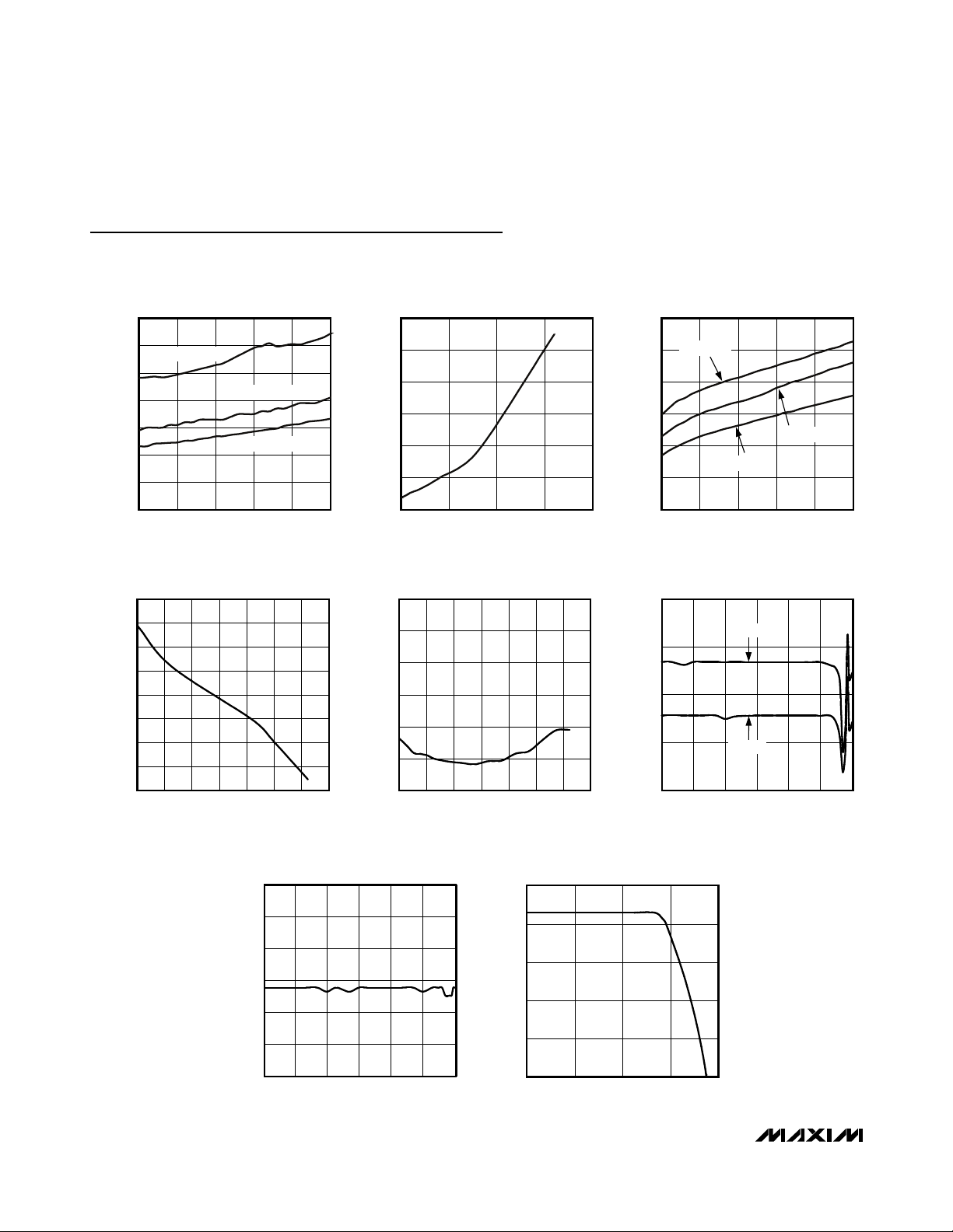
Typical Operating Characteristics
(VCC= 3.3V, TA= +25°C, unless otherwise noted.)
STANDBY SUPPLY CURRENT
vs. SUPPLY VOLTAGE
7
6
5
4
3
SUPPLY CURRENT (µA)
2
1
0
TA = +85°C
3.0 5.5
SUPPLY VOLTAGE (V)
REMOTE TEMPERATURE ERROR
vs. REMOTE DIODE TEMPERATURE
0.8
0.6
0.4
0.2
0
-0.2
-0.4
REMOTE TEMPERATURE ERROR (°C)
-0.6
-0.8
0406020
REMOTE DIODE TEMPERATURE (°C)
TA = +25°C
TA = -40°C
100 120 140
80
AVERAGE SUPPLY CURRENT
vs. CONVERSION RATE
600
500
MAX6638 toc01
400
300
200
SUPPLY CURRENT (µA)
100
0
5.04.54.03.5
020
CONVERSION RATE (Hz)
15105
MAX6638 toc02
SUPPLY CURRENT (µA)
LOCAL TEMPERATURE ERROR
vs. DIE TEMPERATURE
0
MAX6638 toc04
-0.5
-1.0
-1.5
-2.0
LOCAL TEMPERATURE ERROR (°C)
-2.5
-3.0
0608020 40 100 120 140
DIE TEMPERATURE (°C)
MAX6638 toc05
OPERATING SUPPLY CURRENT
vs. SUPPLY VOLTAGE
700
TA = +85°C
650
600
550
500
450
400
3.0 5.5
TA = -40°C
SUPPLY VOLTAGE (V)
TA = +25°C
5.04.54.03.5
TEMPERATURE ERROR
vs. POWER-SUPPLY NOISE FREQUENCY
6
LOCAL
4
2
TEMPERATURE ERROR (°C)
0
-2
0.01 100.1 1 100 1,000 10,000
POWER-SUPPLY NOISE FREQUENCY (kHz)
REMOTE
MAX6638 toc03
MAX6638 toc06
LOCAL TEMPERATURE ERROR
vs. COMMON-MODE NOISE FREQUENCY
0
-1
-2
-3
-4
LOCAL TEMPERATURE ERROR (°C)
-5
-6
0.01 1 100.1 100 1,000 10,000
COMMON-MODE NOISE FREQUENCY (kHz)
MAX6638 toc07
REMOTE TEMPERATURE ERROR
vs. DXP-DXN CAPACITANCE
2
0
-2
-4
-6
REMOTE TEMPERATURE ERROR (°C)
-8
0.01 10.1 10 100
DXP-DXN CAPACITANCE (nF)
MAX6638 toc08
Page 5
Detailed Description
The MAX6638 temperature monitor features dual-port
SMBus access for use in thermal management of
graphics processing unit (GPU) and CPU systems.
Each of the two SMBus serial ports can be accessed
independently by two thermal-monitoring systems with
all dual-port collision-avoidance logic controlled by the
MAX6638. Each SMBus thermal-monitoring channel
(channels 1 and 2) has a corresponding over/undertemperature ALERT_ open-drain output with independently configurable limit registers. Channel 1 includes
an overtemperature indicator (OVERT1) with an initial
set-point limit that is always activated after a power-on
reset (POR). The initial OVERT1 set point can be overwritten after POR by SMBus1 serial programming. The
overtemperature alarm OVERT1 asserts if the set-point
limit is exceeded.
ADC and Multiplexer
The MAX6638 converts temperatures to digital data
either at a programmed rate or in single conversions.
Either SMBus controller can set the programmed rate
with the higher rate setting taking precedence. The
MAX6638 begins conversions at the maximum rate
after POR to provide the OVERT1 output signal assertion for temperatures exceeding the set-point limit. The
temperature conversion results of the two temperature
channels are in integer format. The MSBs of the temperature data are in 8-bit registers (addresses 00h and
01h; see Table 1) that represent the data as 8 bits with
the full-scale reading to indicate a diode fault. The
remaining 3 bits of temperature data are available in
the extended data-registers format with the LSB equal
to +0.125°C (addresses 11h and 10h; see Table 2).
The converted readings are stored in SMBus reading
registers along with the limit-value registers and other
control functions.
MAX6638
Temperature Monitor with
Dual Serial Interface
_______________________________________________________________________________________ 5
Pin Description
Table 1. Temperature Data Format
(RLTS1, RRTS1, RLTS2, RRTS2)
PIN NAME FUNCTION
1V
2 DXP
3DXN
4 OVERT1 Digital Open-Drain Output. OVERT1 indicates an overtemperature condition on channel 1.
5, 7, 12, 13 N.C. No Connection. Not connected internally.
6 I.C. Internally Connected. I.C. must be connected to GND.
8 GND Power-Supply Ground
9 ALERT1 Digital Open-Drain Output. ALERT1 indicates alert condition on channel 1.
10 SDA1 SMBus Data Channel 1. Open-drain output.
11 SCK1 SMBus Clock Channel 1
14 ALERT2 Digital Open-Drain Output. ALERT2 indicates alert condition on channel 2.
15 SDA2 SMBus Data Channel 2. Open-drain output.
16 SCK2 SMBus Clock Channel 2
EP GND Ground. Connect to ground.
CC
Supply Voltage. Bypass VCC to GND with a 0.1µF capacitor. A 47Ω series resistor is recommended for
additional noise filtering, but not required.
Combined Current Source and ADC Positive Input for Remote Diode. If a remote-sensing junction is not
used, connect DXP to DXN.
Combined Current Sink and ADC Negative Input for Remote Diode. DXN is internally biased to a diode
voltage above ground.
TEMPERATURE
(°C)
+145 91 1001 0001
+130 82 1000 0010
+128 80 1000 0000
+25 19 0001 1001
0 00 0000 0000
< 0 00 0000 0000
Diode fault FF 1111 1111
DIGITAL OUTPUT
(hex)
DIGITAL OUTPUT
(bin)
Page 6
MAX6638
Temperature Monitor with
Dual Serial Interface
6 _______________________________________________________________________________________
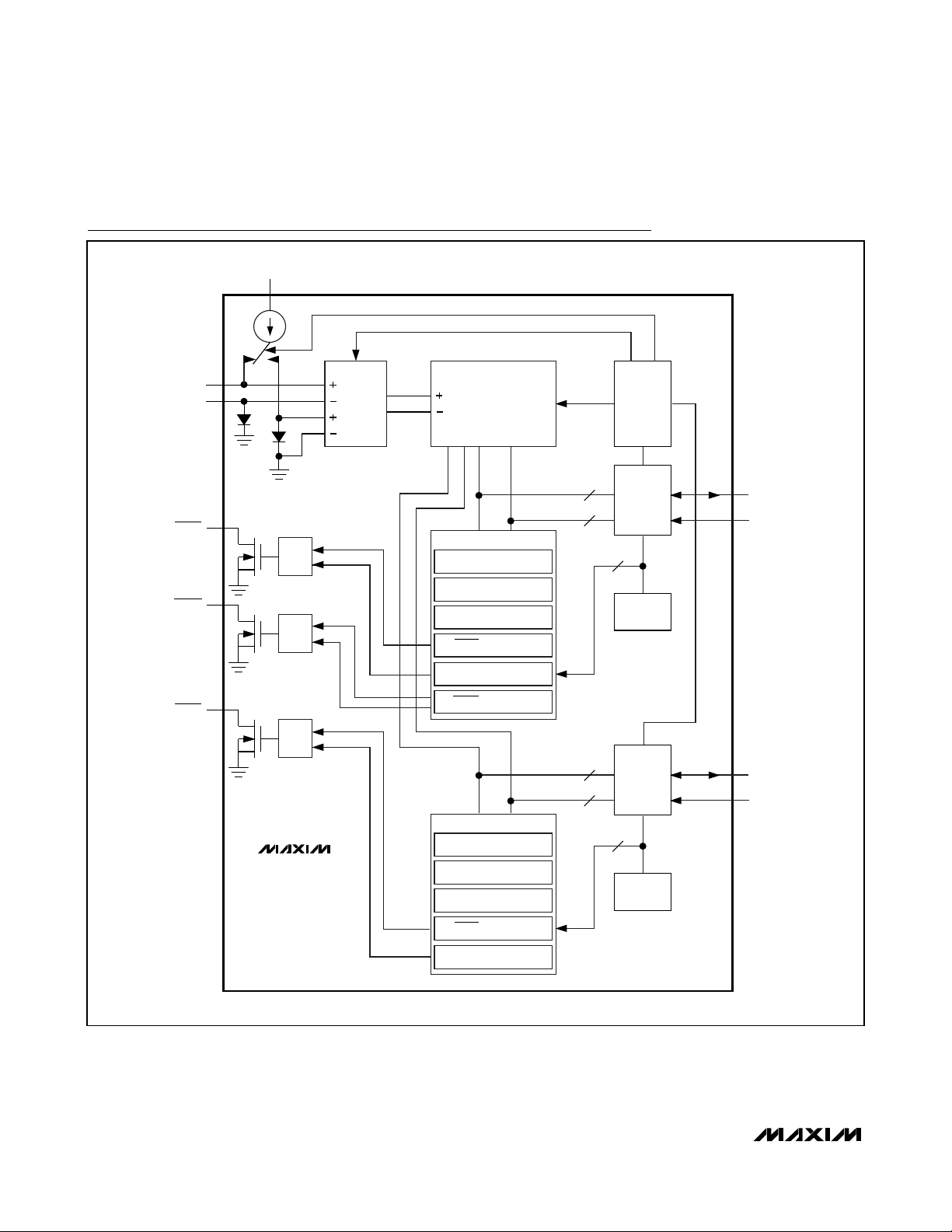
Functional Diagram
V
CC
DXP
DXN
ALERT1
OVERT1
ALERT2
S
Q
R
S
Q
R
S
Q
R
MAX6638
MUX
REMOTE
LOCAL
ADC
REGISTER BANK1
COMMAND BYTE
REMOTE TEMPERATURE
LOCAL TEMPERATURE
ALERT THRESHOLD
ALERT-RESPONSE ADDRESS
OVERT THRESHOLD
REGISTER BANK2
COMMAND BYTE
REMOTE TEMPERATURE
LOCAL TEMPERATURE
CONTROL
LOGIC
SMBus
8
READ
8
WRITE
7
ADDRESS
DECODER
SMBus
8
READ
8
WRITE
7
ADDRESS
DECODER
SDA1
SCK1
SDA2
SCK2
ALERT THRESHOLD
ALERT-RESPONSE ADDRESS
Page 7

The averaging ADC integrates over a 16ms period
(each channel, typical) with excellent noise rejection.
The multiplexer automatically steers bias currents
through the remote and local diodes. The ADC and
associated circuitry measure each diode’s forward voltage and compute the temperature based on this voltage. Both temperature sensors automatically convert
once the conversion process starts, either in free-running (RUN = 0) or single-shot mode. A BUSY status bit
in the status byte indicates that the device is performing
a new conversion. The results of the previous conversion are always available even when the ADC is busy. If
one of the two temperature sensors is not used, the
MAX6638 still performs both measurements and ignores
the results of the unused channel. When not using the
remote-diode temperature sensor, connect DXP to DXN.
The DXP-DXN differential input voltage range is 0.25V to
0.95V. Excess resistance in series with the remote diode
causes a +0.5°C (typ) error per ohm.
The MAX6638 initiates conversion cycling after POR,
after exiting standby mode from either SMBus channel,
and upon one-shot request from either SMBus channel.
One conversion cycle consists of two ADC conversions
(one for the local temperature, one for the remote temperature), a diagnostic check on the remote temperature sensor, loading of data into the read registers,
setting diagnostic flags, and setting ALERT1, ALERT2,
and OVERT1, as required. Figure 1 shows the simplified
timing sequence.
MAX6638
Temperature Monitor with
Dual Serial Interface
_______________________________________________________________________________________ 7
Table 2. Extended Temperature Data
(RLET1, RRET1, RLET2, RRET2)
Figure 1. One Complete ADC Conversion Cycle
Figure 2. Repeating ADC Conversion Cycles for Various Conversion Rate Settings
FRACTIONAL
TEMPERATURE (°C)
0.000 000X XXXX
0.125 001X XXXX
0.250 010X XXXX
0.375 011X XXXX
0.500 100X XXXX
0.675 101X XXXX
0.750 110X XXXX
0.875 111X XXXX
DIGITAL OUTPUT (bin)
ONE CONVERSION CYCLE
ADC LOCAL TEMPERATURE ADC AND DIAGNOSTIC REMOTE TEMPERATURE
START CONVERSION UPDATE REGISTERS DATA AVAILABLE TIME
START
CRCn
CONVERSION
06h
05h
04h
03h
02h
250 500 750 1000 1250 1500 1750 2000
ONE CONVERSION CYCLE
TIME (ms)
Page 8

MAX6638
The MAX6638 allows conversion rates that are 2x multiples of the minimum rate of 0.0625Hz. Figure 2 shows
several different conversion rate settings.
The ADC converts at the higher rate of the two conversions set by SMBus1 and SMBus2 controllers. The controller that sets the higher rate receives a new
conversion at the higher conversion-rate time. The controller that sets the lower rate receives the most recent
conversion result at the lower conversion-rate timing.
Figure 3 shows an example of this. SMBus1 initiates the
ADC converter by selecting conversion rate 06h (4Hz)
prior to SMBus2 initiating a conversion. Then SMBus2
initiates conversions of 05h (2Hz) independent of the
process initiated by SMBus1. The controller accesses
data at its programmed time set by the initiated conversion time. The data presented to SMBus2 is always
ready at the anticipated time, but the data is actually
the result of a previous conversion sequence driven by
the higher conversion rate set by SMBus1.
The first SMBus channel that activates a conversion
sequence always establishes the MAX6638 conversion
cycling. The ADC conversion rates increase and
decrease as set by each of the SMBus controllers with
the higher conversion rate always dominating.
Increasing the conversion rate with the ADC cycling
increases the rate the MAX6638 performs cycles without losing sync of the previously established cycle timing. A decrease in conversion rate reduces the ADC
cycling to the lower rate without losing sync with the
previously set cycle pattern. The ADC cycling pattern is
only reset following a POR event or upon exiting the
standby mode through one of the SMBus controllers’
initiation of cycling or single-shot conversion.
Low-Power Standby Mode
Standby mode reduces the supply current to 3µA (typ)
by disabling the ADC and timing circuitry when both
SMBus controller channels enable standby mode.
Standby mode is enabled only when both SMBus controllers request standby mode. Set each of the RUN bits
to 1 in each corresponding configuration register (see
Tables 3 and 5) to enter standby mode. When one
SMBus controller channel is set to standby mode, the
other conversion rate is automatically set to the active
channel’s conversion rate and mode. The MAX6638
retains all data in the registers and each SMBus interface is active and listening for SMBus commands.
Standby mode is not a shutdown mode. With activity on
either SMBus, the device draws more supply current
(see the Typical Operating Characteristics). In standby
mode, the MAX6638 performs an ADC conversion
sequence through the one-shot command, regardless
of either of the RUN bit statuses, upon receipt of a oneshot command from either SMBus controller.
If the device receives standby commands from both
SMBus controllers during a conversion, the conversion
cycle truncates, and the data from that conversion is
not latched into a temperature register. The previous
data does not change and remains available.
Supply current drawn during the 32ms conversion period
is 800µA (typ). Slowing down the conversion rate reduces
the average supply current (see the Typical Operating
Characteristics). Between conversions, the conversion
rate timer consumes 40µA (typ) of supply current.
SMBus Interface
From a software perspective, the MAX6638 appears as a
set of byte-wide registers that contain temperature data,
Temperature Monitor with
Dual Serial Interface
8 _______________________________________________________________________________________
Figure 3. An Example of ADC Cycling for Two Conversion Rates Set by Each Controllers on SMBus1 and SMBus2
SMBus1 START
CONVERSION
SMBus1 CRC1 = 06h
SMBus2 CRC2 = 05h
ACTUAL DATA
READY FROM
ADC CONVERSIONS
ACTUAL DATA READ
BY SMBus2
CYCLE CYCLE CYCLE CYCLE CYCLE CYCLE CYCLE CYCLE CYCLE
250 500 750 1000 1250 1500 1750 2000
SMBus1 DATA AVAILABLE
CYCLE CYCLE CYCLE CYCLE
SMBus2 START
CONVERSION
SHADED BOXES INDICATE EXPECTED ADC CONVERSION CYCLING AND DATA READINGS OF SMBus2 FROM START CONVERSION
TIME
(ms)
Page 9

threshold limit values, and control. A standard SMBus
2-wire serial interface is used to read temperature data,
write control bits, and set threshold data. The MAX6638
employs four standard SMBus protocols: write byte, read
byte, send byte, and receive byte (Figure 4).
Read the temperature data from the read internal temperature (00h) and read external temperature (01h)
registers of each SMBus channel. The temperature
data format for these registers is 8 bits for each temperature-sensor channel, with the LSB representing 1°C
(Table 1). The temperature data transmits MSB first.
The external extended-temperature register (10h) provides additional 3 bits, extending the data to 11 bits
and the resolution to 0.125°C per LSB (Table 2).
The main temperature register and the extended temperature registers update simultaneously upon completion
of a conversion. To ensure the registers contain the
results of the same conversion of the main temperature
data (MSBs) and the extended temperature data (LSBs),
read the data before a new conversion completes.
Alarm-Threshold Registers
Four registers store ALERT threshold values: one high
temperature (THIGH_) and one low temperature
(TLOW_) limit register each for the local and remote
temperature sensors. If either measured temperature
equals or exceeds the corresponding ALERT_ threshold value, the ALERT_ output asserts.
The MAX6638 local ALERT_ THIGH_ register POR state
is 0101 0101, which corresponds to +85°C, while the
remote ALERT_ THIGH_ register POR state is 0101
1111, which corresponds to +95°C. The POR state of
the local and remote TLOW_ registers for all devices is
0000 0000, corresponding to 0°C.
Two additional registers store remote and local alarm
threshold data corresponding to the OVERT1 output
accessible only through SMBus1. The MAX6638 stores
high-temperature thresholds in these registers. If either
of the measured temperatures equals or exceeds the
corresponding alarm threshold value, the OVERT1 out-
put asserts. The MAX6638 local OVERT1 register POR
state is 0101 0101, corresponding to +85°C, while the
remote OVERT1 register POR state is 0111 1101, corre-
sponding to +125°C.
Diode Fault
A continuity fault detector at DXP detects an open circuit between DXP and DXN, or a DXP short to VCC,
MAX6638
Temperature Monitor with
Dual Serial Interface
_______________________________________________________________________________________ 9
Write Byte Format
Read Byte Format
Send Byte Format
Receive Byte Format
Slave Address: equivalent to chip-select line of
a 3-wire interface
Command Byte: selects to
which register you are writing
Data Byte: data goes into the register
set by the command byte (to set
thresholds, configuration masks, and
sampling rate)
Slave Address: equivalent to chip-select line
Command Byte: selects
from which register you
are reading
Slave Address: repeated
due to change in dataflow direction
Data Byte: reads from
the register set by the
command byte
Command Byte: sends command with no data, usually
used for one-shot command
Data Byte: reads data from
the register commanded
by the last read byte or
write byte transmission;
also used for SMBus alert
response return address
S = Start condition Shaded = Slave transmission
P = Stop condition /// = Not acknowledged
S ADDRESS WR ACK COMMAND
7 bits 8 bits
ACK DATA
8 bits
ACK P
1
S ADDRESS WR ACK COMMAND ACK S ADDRESS RD ACK DATA /// P
8 bits7 bits8 bits7 bits
S ADDRESS WR ACK COMMAND ACK P
7 bits 8 bits
S ADDRESS RD ACK DATA /// P
8 bits7 bits
Figure 4. SMBus Protocols
Page 10

MAX6638
GND, or DXN. If an open or short exists, each of the
external temperature registers contains 1111 1111.
When an open-circuit fault occurs, bit 2 (OPEN) in the
status byte sets to 1. If a fault is present upon powerup, the fault is not indicated until the end of the first
conversion cycle.
ALERT_
Interrupts
The ALERT_ interrupt occurs when the internal or exter-
nal temperature reading exceeds a high- or low-temperature limit (programmed). The ALERT_ output signal
latches and can only clear by either reading the status
register or by successfully responding to an alertresponse address. In both cases, the alert clears if the
temperature fault condition no longer exists. Asserting
ALERT_ does not halt automatic conversion. The open-
drain ALERT_ outputs allow multiple devices to share a
common interrupt line.
The MAX6638 responds to the SMBus alert-response
address, an interrupt pointer return-address feature.
Prior to taking corrective action, always check to ensure
that an interrupt is valid by reading the current temperature.
Alert Fault-Queue Register
In some systems, it is desirable to ignore a single temperature measurement that falls outside the ALERT_
limits. Bits 1 and 2 of the fault queue register (address
22h) determine the number of consecutive temperature
faults necessary to set ALERT_.
Alert-Response Address
The SMBus alert-response interrupt pointer provides
quick fault identification for simple slave devices that
Temperature Monitor with
Dual Serial Interface
10 ______________________________________________________________________________________
Figure 5. SMBus Write Timing Diagram
Figure 6. SMBus Read Timing Diagram
AB CDEFG
t
LOW
SMBCLK
SMBDATA
t
SU:STAtHD:STA
A = START CONDITION
B = MSB OF ADDRESS CLOCKED INTO SLAVE
C = LSB OF ADDRESS CLOCKED INTO SLAVE
D = R/W BIT CLOCKED INTO SLAVE
AB CDEFG HIJ
t
SMBCLK
SMBDATA
t
t
HD:STA
SU:STA
A = START CONDITION
B = MSB OF ADDRESS CLOCKED INTO SLAVE
C = LSB OF ADDRESS CLOCKED INTO SLAVE
D = R/W BIT CLOCKED INTO SLAVE
E = SLAVE PULLS SMBDATA LINE LOW
t
HIGH
LOWtHIGH
t
SU:DAT
E = SLAVE PULLS SMBDATA LINE LOW
F = ACKNOWLEDGE BIT CLOCKED INTO MASTER
G = MSB OF DATA CLOCKED INTO SLAVE
H = LSB OF DATA CLOCKED INTO SLAVE
t
SU:DAT
F = ACKNOWLEDGE BIT CLOCKED INTO MASTER
G = MSB OF DATA CLOCKED INTO MASTER
H = LSB OF DATA CLOCKED INTO MASTER
I = MASTER PULLS DATA LINE LOW
t
HD:DAT
HIJ
I = MASTER PULLS DATA LINE LOW
J = ACKNOWLEDGE CLOCKED INTO SLAVE
K = ACKNOWLEDGE CLOCK PULSE
L = STOP CONDITION
M = NEW START CONDITION
K
J = ACKNOWLEDGE CLOCKED INTO SLAVE
K = ACKNOWLEDGE CLOCK PULSE
L = STOP CONDITION
M = NEW START CONDITION
t
SU:STOtBUF
L
t
SU:STO
LMK
M
t
BUF
Page 11

lack the complex logic needed to be a bus master.
Upon receiving an ALERT_ interrupt signal, the host
master can broadcast a receive-byte transmission to
the alert-response slave address (0001 100). Following
such a broadcast, any slave device generating an
interrupt attempts to identify itself by putting its own
address on the bus.
The alert response can activate several different slave
devices simultaneously. If more than one slave
attempts to respond, bus arbitration rules apply, and
the device with the lower address code wins. The losing device does not generate an acknowledge
response and continues to hold the ALERT_ line low
until cleared. Successful completion of the read alertresponse protocol clears the interrupt latch, provided
the condition that caused the alert no longer exists.
Overtemperature Limit Output
OVERT1 asserts when the temperature rises to a value
stored in one of the OVERT1 limit registers (19h and
20h). It deasserts when the temperature drops below
the stored limit, minus hysteresis. OVERT1 can be used
to activate a cooling fan, send a warning, invoke clock
throttling, or trigger a system shutdown to prevent component damage.
Command-Byte Functions
The 8-bit command-byte register (Table 3) is the master index that points to the various other registers within
the MAX6638. The register’s POR state is 0000 0000,
so a receive-byte transmission (a protocol that lacks
the command byte) that occurs immediately after POR
returns the current local-temperature data.
One-Shot Conversion Cycle
The one-shot command immediately forces a new conversion cycle to begin. If the MAX6638 receives a oneshot command while the MAX6638 is in standby mode
(RUN = 1), a new conversion begins, after which the
device returns to standby mode. If during a conversion
the MAX6638 receives a one-shot command, the
MAX6638 ignores the command; however, the results of
the conversion in progress update the data registers
accordingly.
Configuration-Byte Functions
The configuration-byte register (Tables 3 and 5) is a
read-write register with several functions. Bit 7 masks
interrupts. Bit 6 puts the MAX6638 into a standby (STOP)
mode or autonomous (RUN) mode. The MAX6638 enters
standby mode when both SMBus controllers set the corresponding configuration bits.
Status-Byte Functions
The status-byte register (Tables 3 and 4) indicates
when any temperature threshold is exceeded. This byte
also indicates whether the ADC is converting and if
there is a fault detected in the external sense diode.
After POR, the state of the flag bits are zero, assuming
no alarm conditions are present. The status byte clears
with any successful read of the status byte, after completion of a conversion and if the fault condition no
longer exists. Note that the ALERT_ interrupt latch does
not automatically clear when the status-flag bit indicating the ALERT_ clears.
Registers
The internal registers of the MAX6638 are all 8-bit data
word width and are all accessible through SMBus by
read and write operations.
MAX6638
Temperature Monitor with
Dual Serial Interface
______________________________________________________________________________________ 11
Page 12

MAX6638
Temperature Monitor with
Dual Serial Interface
12 ______________________________________________________________________________________
Table 3. SMBus1 Registers and Command-Byte Bit Assignments
R EG .
A D D R ESS
00h Read Local Tem p S ensor RLTS 1 7 6 5 4 3 2 1 0 00h
01h Read Rem ote Tem p S ensor RRTS 1 7 6 5 4 3 2 1 0 00h
02h Read S tatus Byte RS 1BU S Y LH IGH LLO WRH IGH RLO WFAU LT E OT IOT 00h
03h Read C onfi g ur ati on Byte RC 1M AS K RUN RFU RFU RFU RFU RFU RFU 00h
04h Read C onver si on- Rate Byte RC R17654321000h
05h Read Local ALE RT1 H i g h Li m i tRLAH 1 7 6 5 4 3 2 1 0 55h
06h Read Local ALE RT1 Low Li m i t RLAL1 7 6 5 4 3 2 1 0 00h
07h Read Rem ote ALERT1 H ig h Li m i t RRAH 1 7 6 5 4 3 2 1 0 55h
08h Read Rem ote ALERT1 Low Lim i t RRAL1 7 6 5 4 3 2 1 0 00h
09h Wr i te C onfi g ur ati on Byte WC 1 7 6 5 4 3 2 1 0 00h
0Ah Wr i te C onver si on- Rate Byte WC R17654321008h
0Bh Wr i te Local Al er t- H i g h Li m i tWLAH 1 7 6 5 4 3 2 1 0 55h
0C hWr i te Local Al er t- Low Li m i t WLAL1 7 6 5 4 3 2 1 0 00h
0D hWr i te Rem ote Al er t- H i g h Li m i tWRAH 1 7 6 5 4 3 2 1 0 5Fh
0E hWr i te Rem ote Al er t- Low Li m i tWRAL17654321000
0Fh One- S hot C onver si on OS C 17 6 5 4 3 2 1 0 —
10h Read Local - E xtend ed Tem p RLE T1 7 6 5 4 3 2 1 0 00h
11h Read Rem ote- E xtend ed Tem p RRE T1 7 6 5 4 3 2 1 0 00h
19h Read/Wri te Rem ote OVERT1 Limi tRWRO1765432107D h
20h Read /Wr i te Local OVE RT1 Li m i tRWLO17654321055h
21h Over tem p er atur e H yster esi sH Y S 17 6 5 4 3 2 1 00Ah
22h Wr i te Faul t Queue WFQ 1 7 6 5 4 3 2 1 0 80h
FE hRead M anufactur er ID RM ID 765432104D h
FFh Read D evi ce ID RD ID 7654321078h
R EG IST ER NA M EA B B R .
7 6 5 4 3 2 1 0
B IT
PO R
VA L U E
Page 13

MAX6638
Temperature Monitor with
Dual Serial Interface
______________________________________________________________________________________ 13
Table 4. Read Status-Byte (RS1) Bit Assignments (02h)
Table 5. Read Configuration-Byte (RC1) Bit Assignments (03h)
Table 6. Conversion-Rate Control-Byte
(RCR1 and WCR1) Bit Assignments
(04h and 0Ah)
BIT NAME POR STATE FUNCTION
7 BUSY 0 ADC is busy converting when 1.
6 LHIGH 0
5 LLOW 0
4 RHIGH 0
3 RLOW 0
2 OPEN 0
1 EOT 0 A 1 indicates the remote temperature exceeds the external OVERT1 threshold.
0 IOT 0 A 1 indicates the local temperature exceeds the external OVERT1 threshold.
Local High-Temperature Alarm. A 1 indicates a local high-temperature fault. Clears with a
POR or readout of the status byte if the fault condition no longer exists.
Local Low-Temperature Alarm. A 1 indicates a local low-temperature fault. Clears with a POR
or readout of the status byte if the fault condition no longer exists.
Remote High-Temperature Alarm. A 1 indicates a remote high-temperature fault. Clears with
a POR or readout of the status byte if the fault condition no longer exists.
Remote Low-Temperature Alarm. A 1 indicates a remote low-temperature fault. Clears with a
POR or readout of the status byte if the fault condition no longer exists.
A 1 indicates DXN and DXP are open. Clears with a POR or readout of the status byte if the
open condition no longer exists.
BIT NAME POR STATE FUNCTION
7 MASK 0 Masks ALERT1 interrupts when set to 1.
6 RUN 0
5–0 RFU 0 Reserved for future use.
Standby-Mode Control Bit. If set to 1, standby mode enables and enters if the standby-mode
control bit (RUN) for channel 2 is also set.
BIT DATA CONVERSION RATE (Hz)
7–0 00h 0.0625
7–0 01h 0.125
7–0 02h 0.25
7–0 03h 0.5
7–0 04h 1
7–0 05h 2
7–0 06h 4
7–0 07h 8
7–0 08h 16
7–0 09–FFh Reserved
Page 14

MAX6638
Temperature Monitor with
Dual Serial Interface
14 ______________________________________________________________________________________
Table 7. SMBus2 Registers and Command-Byte Bit Assignments
R EG .
A D D R ESS
00h Read Local Tem p S ensor RLTS 2 7 6 5 4 3 2 1 0 00h
01h Read Rem ote Tem p S ensor RRTS 2 7 6 5 4 3 2 1 0 00h
02h Read S tatus Byte RS 2BU S Y LH IGH LLO WRH IGH RLO WFAU LT RFU RFU 00h
03h Read C onfi g ur ati on Byte RC 2M AS K RUN RFU RFU RFU RFU RFU RFU 00h
04h Read C onver si on- Rate Byte RC R27654321000h
05h Read Local ALE RT1 H i g h Li m i tRLAH 2 7 6 5 4 3 2 1 0 55h
06h Read Local ALE RT1 Low Li m i t RLAL2 7 6 5 4 3 2 1 0 00h
07h Read Rem ote ALERT1 H ig h Li m i t RRAH 2 7 6 5 4 3 2 1 0 5Fh
08h Read Rem ote ALERT1 Low Lim i t RRAL2 7 6 5 4 3 2 1 0 00h
09h Wr i te C onfi g ur ati on Byte WC 2 7 6 5 4 3 2 1 0 00h
0Ah Wr i te C onver si on Rate Byte WC R27654321008h
0Bh Wr i te Local Al er t- H i g h Li m i tWLAH 2 7 6 5 4 3 2 1 0 55h
0C hWr i te Local Al er t- Low Li m i t WLAL2 7 6 5 4 3 2 1 0 00h
0D hWr i te Rem ote Al er t- H i g h Li m i tWRAH 2 7 6 5 4 3 2 1 0 5Fh
0E hWr i te Rem ote Al er t- Low Li m i t WRAL2 7 6 5 4 3 2 1 0 00h
0Fh One- S hot C onver si on OS C 27 6 5 4 3 2 1 0 —
10h Read Local - E xtend ed Tem p RLE T2 7 6 5 4 3 2 1 0 00h
11h Read Rem ote- E xtend ed Tem p RRE T2 7 6 5 4 3 2 1 0 00h
19h Read/Wri te Rem ote OVERT1 Limi tRWRO2765432107D h
20h Read /Wr i te Local OVE RT1 Li m i tRWLO27654321055h
21h Over tem p er atur e H yster esi sH Y S 27 6 5 4 3 2 1 00Ah
22h Wr i te Faul t Queue WFQ 2 7 6 5 4 3 2 1 0 80h
FE hRead M anufactur er ID RM ID 765432104D h
FFh Read D evi ce ID RD ID 7654321078h
R EG IST ER NA M EA B B R .
7 6 5 4 3 2 1 0
B IT
PO R
VA L U E
Page 15

MAX6638
Temperature Monitor with
Dual Serial Interface
______________________________________________________________________________________ 15
Table 8. Read Status-Byte (RS2) Bit Assignments (02h)
Table 9. Read Configuration-Byte (RC2) Bit Assignments (03h)
Table 11. Slave Addresses
Table 10. Conversion-Rate Control-Byte
(RCR2 and WCR2) Bit Assignments
(04h and 0Ah)
BIT NAME POR STATE FUNCTION
7 BUSY 0 ADC is busy converting when 1.
6 LHIGH 0
5 LLOW 0
4 RHIGH 0
3 RLOW 0
2 OPEN 0
1 RFU 0 Reserved for future use.
0 RFU 0 Reserved for future use.
Local High-Temperature Alarm. A 1 indicates a local high-temperature fault. Clears with a
POR or readout of the status byte if the fault condition no longer exists.
Local Low-Temperature Alarm. A 1 indicates a local low-temperature fault. Clears with a POR
or readout of the status byte if the fault condition no longer exists.
Remote High-Temperature Alarm. A 1 indicates a remote high-temperature fault. Clears with
a POR or readout of the status byte if the fault condition no longer exists.
Remote Low-Temperature Alarm. A 1 indicates a remote low-temperature fault. Clears with a
POR or readout of the status byte if the fault condition no longer exists.
A 1 indicates DXN and DXP are open. Clears with a POR or a read of the status byte if the
open condition no longer exists.
BIT NAME POR STATE FUNCTION
7 MASK 0 Masks ALERT2 interrupts when set to 1.
6 RUN 0
5–0 RFU 0 Reserved for future use.
Standby-Mode Control Bit. If set to 1, standby mode is enabled and is entered if or when the
standby-mode control bit (RUN) for channel 1 is also set.
BIT DATA CONVERSION RATE (Hz)
7–0 00h 0.0625
7–0 01h 0.125
7–0 02h 0.25
7–0 03h 0.5
7–0 04h 1
7–0 05h 2
7–0 06h 4
7–0 07h 8
7–0 08h 16
7–0 09–FFh Reserved
PART SMBus CHANNEL SLAVE ADDRESS
MAX6638ATC
1 1001 101
2 1001 101
Page 16

MAX6638
Temperature Monitor with
Dual Serial Interface
16 ______________________________________________________________________________________
Applications Information
Remote-Diode Selection
The MAX6638 can directly measure the die temperature of CPUs and other ICs that have on-board temperature-sensing diodes (see the Typical Operating
Circuit), or it can measure the temperature of a discrete
diode-connected transistor.
Effect of Ideality Factor
The accuracy of the remote temperature measurements
depends on the ideality factor (n) of the remote diode
(which is actually a transistor). The MAX6638 is optimized for n = 1.008. If a sense transistor with a different
ideality factor is used, the output data is different.
Fortunately, the difference is predictable.
Assume a remote-diode sensor designed for a nominal
ideality factor n
NOMINAL
is used to measure the tem-
perature of a diode with a different ideality factor n
1
.
The measured temperature TMcan be corrected using:
where temperature is measured in Kelvin.
The following example uses the MAX6638 with a CPU
that has an ideality factor of 1.002. If the diode has
negligible series resistance, the measured data is related to the real temperature as follows:
For a real temperature of +85°C (358.15K), the converted and quantized temperature data is +82.875°C
(356.03K), which is an error of -2.12°C. Using the correction formula above, the corrected temperature data
is +85.0°C (358.16K).
Effect of Series Resistance
Series resistance (RS) in a sense diode contributes additional errors. For nominal diode currents of 10µA and
100µA, the change in the measured voltage due to RSis:
∆VM= RS(100µA - 10µA) = 90µA x RS.
A 1°C corresponds to 198.6µV, series resistance contributes a temperature offset of:
Assume that the diode measured has a 3Ω series resistance. The series resistance contributes an offset of:
The effects of the ideality factor and series resistance
are additive. If the diode has a 1.002 ideality factor and
3Ω series resistance the total offset can be calculated
by adding error due to series resistance with error due
to ideality factor:
1.36°C - 2.12°C = -0.77°C
for a diode temperature of +85°C.
In this example, the effects of series resistance and
ideality factor partially cancel each other.
Discrete Remote Diodes
When the remote-sensing diode is a discrete transistor,
short the collector to the base. Table 12 lists examples
of discrete transistors that are appropriate for use with
the MAX6638. Avoid violating the A/D input voltage
range by using a small-signal transistor with a relatively
high forward voltage. The forward voltage at the highest
expected temperature must be greater than 0.25V at
10µA, and the forward voltage at the lowest expected
temperature must be less than 0.95V at 100µA. Do not
use large power transistors. Ensure that the base resistance is less than 100Ω. Tight specifications for forward
current gain (50 < ß < 150, for example) indicate that the
manufacturer has good process controls and that the
device has consistent VBE characteristics.
ADC Noise Filtering
The ADC is an integrating type with inherently good
noise rejection, especially of low-frequency signals, such
as 60Hz/120Hz power-supply hum. Micropower operation places constraints on high-frequency noise rejection;
3 0 453 1 36ΩΩ×
°
=°..
C
C
90
198 6
0 453
µµV
V
C
Ω
Ω
Ω
.
.=
°
TT
n
n
TT
ACTUAL M
NOMINAL
MM
=
⎛
⎝
⎜
⎞
⎠
⎟
=
⎛
⎝
⎜
⎞
⎠
⎟
=
()
1
1 008
1 002
1 00599
.
.
.
TT
n
n
M ACTUAL
NOMINAL
=
⎛
⎝
⎜
⎞
⎠
⎟
1
Table 12. Remote-Sensor Transistor
Manufacturers
Note: Discrete transistors must be diode connected (base
shorted to collector).
MANUFACTURER MODEL
Central Semiconductor (USA) CMPT3906
Rohm Semiconductor (USA) SST3906
Samsung (Korea) KST3906-TF
Siemens (Germany) SMBT3906
Zetex (England) FMMT3906CT-ND
Page 17

therefore, careful PC board layout and proper external
noise filtering are required for high-accuracy remote
measurements in electrically noisy environments.
Filter high-frequency EMI at DXP and DXN with an
external 2200pF capacitor. This value can be increased
to approximately 3300pF (max), including cable capacitance. Capacitance > 3300pF introduces errors due to
the rise time of the switched current source. Typically
noise sources cause the ADC measurements to be
higher than the actual temperature, approximately by
+1°C to +10°C, depending on the frequency and
amplitude.
PC Board Layout
Follow these guidelines to reduce the measurement
error of the temperature sensor:
1) Place the MAX6638 as close as is practical to the
remote diode. In noisy environments, such as a
computer motherboard, this distance can be 4in to
8in (typ). This length can be increased if the worst
noise sources are avoided. Noise sources include
CRTs, clock generators, memory buses, and
ISA/PCI buses.
2) Do not route the DXP-DXN lines next to the deflection coils of a CRT. Also, do not route the traces
across fast digital signals, which can easily introduce a 30°C error, even with good filtering.
3) Route the DXP and DXN traces in parallel and in close
proximity to each other, away from any higher voltage
traces, such as 12V DC. Leakage currents from PC
board contamination must be dealt with carefully since
a 20MΩ leakage path from DXP to ground causes
approximately a 1°C error. If high-voltage traces are
unavoidable, connect guard traces to GND on either
side of the DXP-DXN traces (Figure 4).
4) Route through as few vias and crossunders as possible to minimize copper/solder thermocouple
effects.
5) When introducing a thermocouple, make sure that
both the DXP and the DXN paths have matching
thermocouples. A copper-solder thermocouple
exhibits 3µV/°C, and takes approximately 200µV of
voltage error at DXP-DXN to cause a 1°C measurement error. Adding a few thermocouples causes a
negligible error.
6) Use wide traces. Narrow traces are more inductive
and tend to pick up radiated noise. The 10-mil withstand spacing recommended in Figure 4 is not
absolutely necessary, as it offers only a minor
improvement in leakage and noise over narrow
traces. Use wider traces when practical.
7) Add a 200Ω resistor in series with VCCfor best
noise filtering (see the Typical Operating Circuit).
8) Copper cannot be used as an EMI shield; only ferrous materials such as steel work well. Placing a
copper ground plane between the DXP-DXN traces
and traces carrying high-frequency noise signals
does not help reduce EMI.
PC Board Layout Checklist
• Place the MAX6638 close to the remote-sense junction.
• Keep traces away from high voltages (+12V bus).
• Keep traces away from fast data buses and CRTs.
• Use recommended trace widths and spacings.
• Place a ground plane under the traces.
• Use guard traces flanking DXP and DXN and connecting to GND.
• Add a 47Ω resistor in series with VCCfor best noise
filtering (see the Typical Operating Circuit).
• Place the noise filter and a 0.1µF VCCbypass
capacitor close to the MAX6638.
Twisted-Pair and Shielded Cables
Use a twisted-pair cable to connect the remote sensor
for remote-sensor distance longer than 8in, or in very
noisy environments. Twisted-pair cable lengths can be
between 6ft and 12ft before noise introduces excessive
errors. For longer distances, the best solution is a
shielded twisted pair like that used for audio microphones. For example, Belden 8451 works well for distances up to 100ft in a noisy environment. At the
device, connect the twisted pair to DXP and DXN and
the shield to GND. Leave the shield unconnected at the
remote sensor.
For very long cable runs, the cable’s parasitic capacitance often provides noise filtering, so the 2200pF
capacitor can often be removed or reduced in value.
Cable resistance also affects remote-sensor accuracy.
For every 1Ω of series resistance, the error is approximately 0.5°C.
Thermal Mass and Self-Heating
When sensing local temperature, these devices are
intended to measure the temperature of the PC board
to which the devices are soldered. The leads provide a
good thermal path between the PC board traces and
the die. Thermal conductivity between the die and the
ambient air is poor by comparison, making air temperature measurements impractical. Because the thermal
mass of the PC board is far greater than that of the
MAX6638
Temperature Monitor with
Dual Serial Interface
______________________________________________________________________________________ 17
Page 18

MAX6638
MAX6638, the device follows temperature changes on
the PC board with little or no perceivable delay.
When measuring the temperature of a CPU or another IC
with an on-chip sense junction, thermal mass has virtually no effect; the measured temperature of the junction
tracks the actual temperature within a conversion cycle.
When measuring temperature with discrete remote sensors, smaller packages, such as SC70s or SOT23s, yield
the best thermal response times. Take care to account
for thermal gradients between the heat source and the
sensor, and ensure that stray air currents across the sensor package do not interfere with measurement accuracy. Self-heating does not significantly affect
measurement accuracy. Remote-sensor self-heating due
to the diode current source is negligible. For the local
diode, the worst-case error occurs when autoconverting
at the fastest rate and simultaneously sinking maximum
current at the ALERT1 output. For example, with V
CC
5.5V, at a 16Hz conversion rate and with ALERT1 sinking
1mA, the typical power dissipation is:
5.5V x 800µA + 0.4V x 1.0mA = 4.8mW
θ
J-A
for the 16-pin, 4mm x 4mm TQFN package is
59.3°C/W, so assuming no copper PC board heat sinking, the resulting temperature rise is:
∆T = 4.8mW x 59.3°C/W = +0.283°C.
Even under nearly worst-case conditions, it is difficult to
introduce a significant self-heating error.
Temperature Monitor with
Dual Serial Interface
18 ______________________________________________________________________________________
Typical Operating Circuit
Chip Information
PROCESS: BiCMOS
3.3V
Ω
47
10k
SDA1
SCK1
2200pF
0.1µF
DXP
DXN
V
CC
Ω
Ω
Ω
Ω
10k
10k
Ω
Ω
10k
10k
Ω
10k
10k
DATA FROM/TO µP1
CLOCK FROM µP1
INTERRUPT TO µP1
TO FAN DRIVER OR SYSTEM SHUTDOWN
DATA FROM/TO µP2
CLOCK FROM µP2
INTERRUPT TO µP2
GND
ALERT1
OVERT1
SDA2
SCK2
ALERT2
µ
P
MAX6638
Page 19

MAX6638
Temperature Monitor with
Dual Serial Interface
Maxim cannot assume responsibility for use of any circuitry other than circuitry entirely embodied in a Maxim product. No circuit patent licenses are
implied. Maxim reserves the right to change the circuitry and specifications without notice at any time.
Maxim Integrated Products, 120 San Gabriel Drive, Sunnyvale, CA 94086 408-737-7600 ____________________ 19
© 2006 Maxim Integrated Products Printed USA is a registered trademark of Maxim Integrated Products, Inc.
Package Information
(The package drawing(s) in this data sheet may not reflect the most current specifications. For the latest package outline information,
go to www.maxim-ic.com/packages
.)
Springer
24L QFN THIN.EPS
PACKAGE OUTLINE,
12, 16, 20, 24, 28L THIN QFN, 4x4x0.8mm
21-0139
1
E
2
PACKAGE OUTLINE,
12, 16, 20, 24, 28L THIN QFN, 4x4x0.8mm
21-0139
2
E
2
 Loading...