

General Description
The MAX6633/MAX6634/MAX6635 combine a temperature sensor, a programmable overtemperature alarm,
and an SMBus™/I
2
C™-compatible serial interface into
a single package. They convert their die temperatures
into digital values using internal analog-to-digital converters (ADCs). The result of the conversion is then held
in a temperature register as a 12-bit + sign value, allowing 0.0625°C resolution, readable at any time through
the serial interface. The devices are capable of reading
temperatures up to +150°C.
The MAX6633/MAX6634/MAX6635 feature a shutdown
mode that saves power by turning off everything except
the power-on reset (POR) and the serial interface. The
devices can be configured to separate addresses,
allowing multiple devices to be used on the same bus.
The MAX6633 has four address pins, allowing up to 16
devices to be connected to a single bus. The MAX6634
has three address pins, allowing up to eight devices to
be connected to a single bus. The MAX6635 has two
address pins, allowing up to four devices to be connected to a single bus.
The MAX6633/MAX6634/MAX6635 make temperature
data available for transfer over the serial interface. The
MAX6634 incorporates a dual-mode ALERT output
(open drain) and can serve as an upgraded alternative
to the LM75. The MAX6635 includes an ALERT output
and an OVERT output (both open drain) and can function as an upgraded replacement for the LM76 in most
applications. The MAX6634/MAX6635 feature user-programmable temperature thresholds. All three devices
come in an 8-pin SO package.
Applications
Battery Temperature Alarms
PC Temperature Control
Automotive Equipment
Features
♦ +3V to +5.5V Supply Range
♦ Accuracy
±1°C max (0°C to +50°C)
±1.5°C max (-20°C to +85°C)
±2.5°C max (-40°C to +125°C)
±2.5°C typ (+150°C)
♦ User-Programmable Temperature Thresholds
(MAX6634/MAX6635)
♦ User-Configurable Alarm Output(s)
(MAX6634/MAX6635)
♦ Ability to Respond to SMBus/I
2
C-Compatible Alert
Response Address (MAX6634/MAX6635)
♦ OVERT Output for System Shutdown (MAX6635)
♦ Multiple Devices per Bus
16 devices (MAX6633)
8 devices (MAX6634)
4 devices (MAX6635)
MAX6633/MAX6634/MAX6635
12-Bit Plus Sign Temperature Sensors with
SMBus/I2C-Compatible Serial Interface
________________________________________________________________
Maxim Integrated Products
1
Ordering Information
19-2120; Rev 0; 8/01
For pricing, delivery, and ordering information, please contact Maxim/Dallas Direct! at
1-888-629-4642, or visit Maxim’s website at www.maxim-ic.com.
EVALUATION KIT
AVAILABLE
SMBus is a trademark of Intel Corp.
I
2
C is a trademark of Philips Corp.
V
CC
V
CC
SCL
SDA
1
5
8
2
3
TO SYSTEM
SHUTDOWN
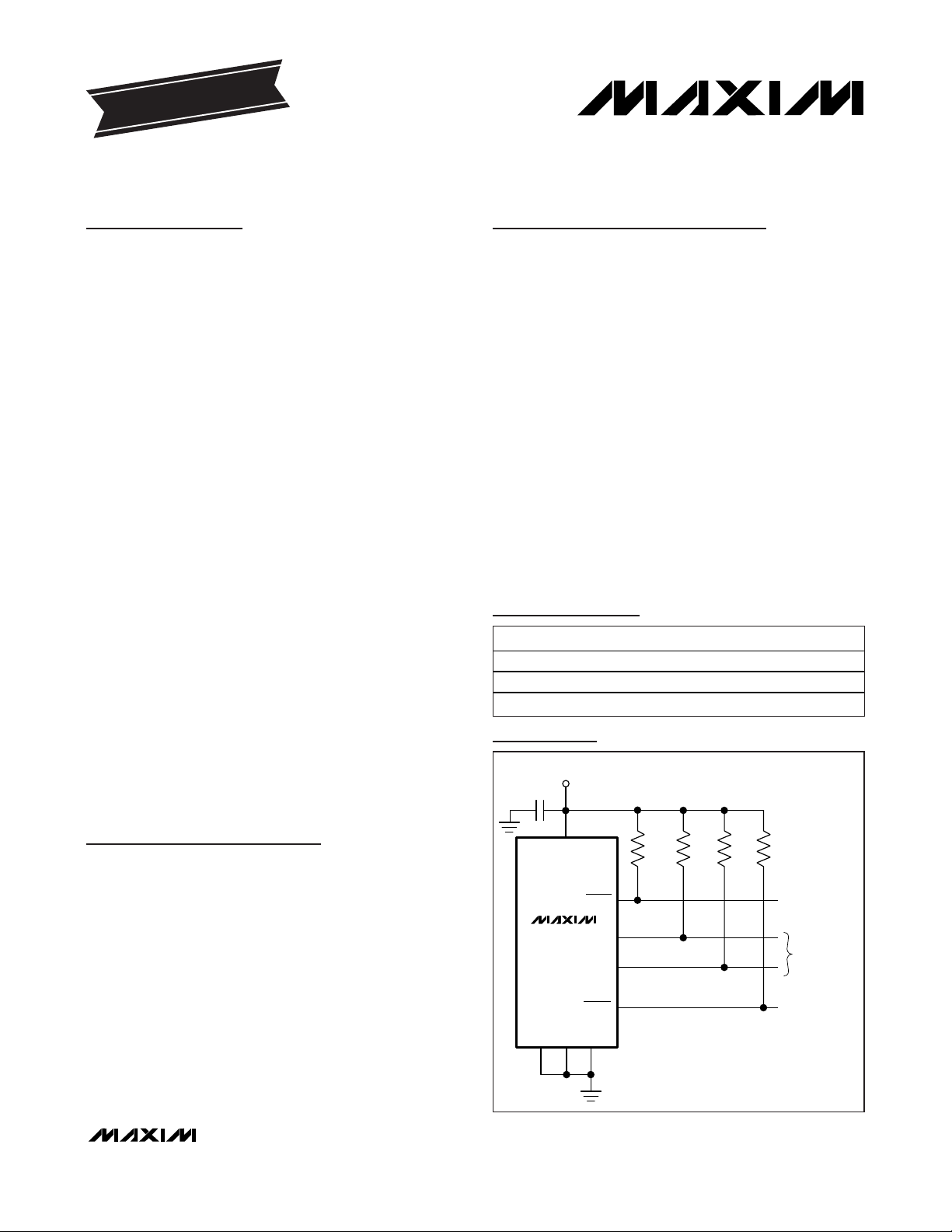
A0 A1 GND
+3.0V TO +5.5V
0.1μF
ALERT
OVERT
MAX6635
467
10kΩ 1kΩ 1kΩ 10kΩ
TO INTERRUPT
CONTROLLER
TO SMBus/I
2
C
MASTER
Typical Operating Circuit
Pin Configurations appear at end of data sheet.
PART TEMP. RANGE PIN-PACKAGE
MAX6633MSA -55°C to +150°C 8 SO
MAX6634MSA -55°C to +150°C 8 SO
MAX6635MSA -55°C to +150°C 8 SO
MAX6633/MAX6634/MAX6635
12-Bit Plus Sign Temperature Sensors with
SMBus/I2C-Compatible Serial Interface
2 _______________________________________________________________________________________
ABSOLUTE MAXIMUM RATINGS
ELECTRICAL CHARACTERISTICS
(VCC= +3.0V to +5.5V, TA= -55°C to +125°C, unless otherwise noted. Typical values are VCC= +3.3V, TA= +25°C, unless otherwise noted.)
Stresses beyond those listed under “Absolute Maximum Ratings” may cause permanent damage to the device. These are stress ratings only, and functional
operation of the device at these or any other conditions beyond those indicated in the operational sections of the specifications is not implied. Exposure to
absolute maximum rating conditions for extended periods may affect device reliability.
VCC, SDA, SCL......................................................-0.3V to +6.0V
All Other Pins ................................................-0.3V to V
CC
+0.3V
SDA, ALERT, OVERT Current .............................-1mA to +50mA
ESD Protection (Human Body Model)................................2000V
Continuous Power Dissipation (T
A
= +70°C)
8-Pin SO (derate 5.88mW/°C above +70°C)................471mW
Junction Temperature......................................................+150°C
Operating Temperature Range .........................-55°C to +150°C
Storage Temperature Range .............................-65°C to +150°C
Lead Temperature (soldering, 10s) ................................+300°C
TEMPERATURE-TO-DIGITAL CONVERTER CHARACTERISTICS
Supply Range V
PARAMETER SYMBOL CONDITIONS MIN TYP MAX UNITS
CC
0°C ≤ T
= ≤ +50°C, VCC = +3.3V -1.0 ±0.4 +1.0
A
3.0 5.5 V
-20°C ≤ T
Accuracy (Note 1)
Power-Supply Rejection Ratio PSRR 0.2 0.5 °C/V
-40°C ≤ T
T
= -55°C, VCC = +3.3V ±1.5 +2.8
A
= +150°C, VCC = +3.3V ±2.5
T
A
= ≤ +85°C, VCC = +3.3V -1.5 ±0.6 +1.5
A
= ≤ 125°C, VCC = +3.3V -2.5 ±1.0 +2.5
A
POR Threshold Hysteresis 90 mV
Supply Current in Shutdown
Average Operating Current
Peak Operating Current (Note 2)
VCC = +3.0V, SMBus inactive 12 20
= +5.5V, SMBus inactive 20 30
V
CC
VCC = +3.0V, SMBus inactive 150
V
= +5.5V, SMBus inactive 200
CC
VCC = +3.0V, SMBus inactive 270 350
V
= +5.5V, SMBus inactive 350 700
CC
Conversion Rate 1.4 2 2.4 Hz
DIGITAL INTERFACE
Logic Input Low Voltage V
Logic Input High
Voltage
Input Leakage Current I
I_LEAK
Output Low Sink Current I
Output Leakage Current I
O_LEAK
Input Capacitance C
V
OL
VCC = +3.0V to +5.5V 0.65 V
IL
VCC = +3V 2.2 V
IH
VCC = +5.5V 2.4
VIN = GND or V
VOL = 0.6V (SMBDATA,
ALERT, OVERT)
ALERT, OVERT at V
IN
CC
6mA
CC
5pF
°C
µA
µA
µA
±1µA
±1µA
MAX6633/MAX6634/MAX6635
12-Bit Plus Sign Temperature Sensors with
SMBus/I2C-Compatible Serial Interface
_______________________________________________________________________________________ 3
ELECTRICAL CHARACTERISTICS (continued)
(VCC= +3.0V to +5.5V, TA= -55°C to +125°C, unless otherwise noted. Typical values are VCC= +3.3V, TA= +25°C, unless otherwise noted.)
Note 1: Guaranteed by design and characterization.
Note 2: Peak operating current measured during conversion. See Figure 4.
Note 3: Guaranteed by design, not production tested.
Note 4: A master device must provide a hold time of at least 300ns for the SDA signal in order to bridge the undefined region of
SCL’s falling edge.
SMBus TIMING (Note 3, Figures 1, 2, and 3)
Serial Clock Frequency f
Bus Free Time Between STOP
and START Condition
START Condition Setup Time 4.7 µs
Repeat START Condition Setup
Time
START Condition Hold Time t
STOP Condition Setup Time t
Data Setup Time t
Data Hold Time (Note 4) t
Receive SCL/SDA Rise Time t
SCL/SDA Fall Time (Note 4) t
Clock Low Period t
Clock High Period t
SMBus Timeout 25 48 ms
PARAMETER SYMBOL CONDITIONS MIN TYP MAX UNITS
10 100 kHz
4.7 µs
300 ns
1µs
300 ns
SCL
t
BUF
t
SU:STA
HD:STA
SU:STO
SU: DAT
HD: DAT
R
F
LOW
HIGH
90% to 90% 4.7 µs
10% of SMBDATA to 90% of SMBCLK 4 µs
90% of SMBCLK to 10% of SMBDATA 4 µs
90% of SMBDATA to 10% of SMBCLK 250 ns
10% to 10% 4.7 µs
90% to 90% 4 µs
MAX6633/MAX6634/MAX6635
12-Bit Plus Sign Temperature Sensors with
SMBus/I2C-Compatible Serial Interface
4 _______________________________________________________________________________________
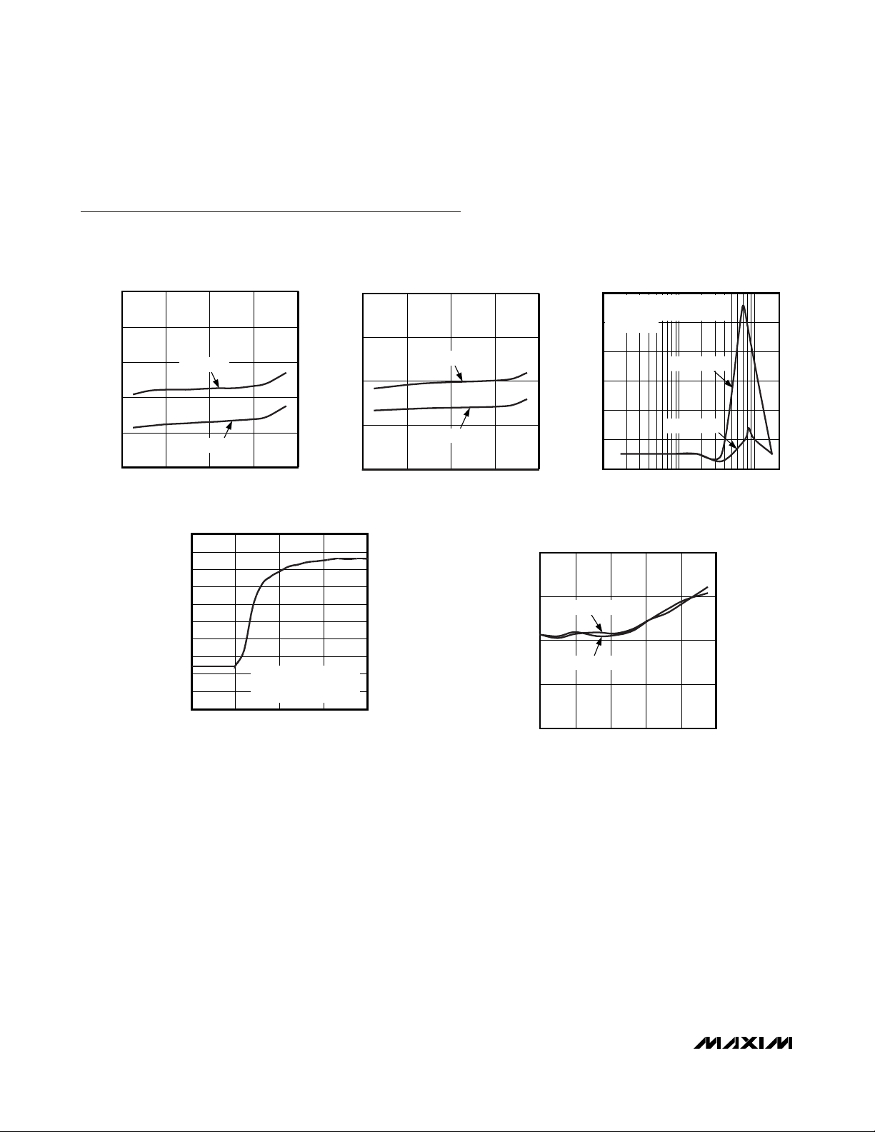
Typical Operating Characteristics
(VCC= +3.3V, TA= +25°C, unless otherwise noted.)
50
40
30
20
0
-55 550
110
165
SHUTDOWN SUPPLY CURRENT
vs. TEMPERATURE
MAX6633/4/5 toc01
TEMPERATURE (°C)
SHUTDOWN SUPPLY CURRENT (μA)
10
VCC = +5.5V
VCC = +3.3V
400
300
200
100
0
-55 550 110 165
AVERAGE SUPPLY CURRENT
vs. TEMPERATURE
MAX6633/4/5 toc02
TEMPERATURE (°C)
AVERAGE SUPPLY CURRENT (μA)
VCC = +5.5V
VCC = +3.3V
5
-1
10 10k 10M
TEMPERATURE ERROR
vs. SUPPLY NOISE FREQUENCY
0
MAX6633/4/5 toc03
SUPPLY NOISE FREQUENCY (Hz)
TEMPERATURE ERROR (°C)
3
2
1
4
VIN = SQUARE WAVE APPLIED TO
V
CC
WITH NO BYPASS
CAPACITOR
VIN = 200mVp-p
VIN = 200mVp-p
0
30
20
10
40
50
60
70
80
90
100
0 5 10 15 20
RESPONSE TO THERMAL SHOCK
MAX6633/4/5 toc04
TIME (s)
TEMPERATURE (°C)
VCC = +5.5V
DEVICE IMMERSED IN +85°C
FLUORINERT BATH
3
2
0
-2
-3
-40 400 80 120 160
TEMPERATURE ERROR
vs. TEMPERATURE
MAX6633/4/5 toc05
TEMPERATURE (°C)
TEMPERATURE ERROR (°C)
VCC = +3.3V
VCC = +5.5V
Detailed Description
The MAX6633/MAX6634/MAX6635 continuously convert their die temperatures into digital values using their
integrated ADCs. The resulting data is readable at any
time through the SMBus/I
2
C-compatible serial interface.
The device functions as a slave on the SMBus interface, supporting Write Byte, Write Word, Read Byte,
and Read Word commands. Separate addresses can
be configured using the individual address pins.
Figures 5, 6, and 7 show the functional diagrams of the
MAX6633/MAX6634/MAX6635, respectively.
SMBus/I2C-Compatible Operation
The MAX6633/MAX6634/MAX6635 are readable and
programmable through their SMBus/I2C-compatible
serial interface. Figures 1, 2, and 3 show the timing
details of the clock (SCL) and data (SDA) signals. The
devices function as slaves on the SMBus and support
Write Byte, Write Word, Read Byte, and Read Word
commands. Figure 8 is the MAX6633/MAX6634/
MAX6635 programmer’s model.
Addressing
Separate addresses can be configured using the individual address pins. The address of each device is
selected by connecting the address (A_) pins to one of
two potentials: GND or VCC. The MAX6635 makes two
address pins available (A0, A1), allowing up to four
devices to be connected to a single bus line. The
MAX6634 makes three address pins available (A0, A1,
A2), allowing up to eight devices to be connected to a
single bus line. The MAX6633 makes four address pins
available (A0, A1, A2, A3), allowing as many as 16
devices to be connected to a single bus line. Table 1
shows the full SMBus/I
2
C address for each device type.
Control Registers (MAX6633)
Three registers control the operation of the MAX6633
(Figure 5 and Tables 2 through 6). The Pointer register
is the first addressed and determines which of the other
two registers is acted upon. The other two are the
Temperature and Configuration registers. The temperature value is stored as 12 bits plus a sign bit, read only,
and contains the latest temperature data. The true register length is 16 bits, with the lower 3 unused in this
part. The digital temperature data contained in the temperature register is in °C, using a two’s-complement
format with 1LSB corresponding to 0.0625°C.
The Configuration register is 8 bits, read/write, and
contains the SMBus timeout disable bit, fault queue
enable bit, and the shutdown bit.
Control Registers (MAX6634)
Six registers control the operation of the MAX6634
(Figure 6 and Tables 2 through 7). The pointer register
is the first addressed and determines which of the other
five registers is acted upon. The other five are the
Temperature, Configuration, High-Temperature
(T
HIGH
), Low-Temperature (T
LOW
), and Hysteresis
(T
HYST
) registers. The temperature value is stored as
12 bits plus a sign bit, read only, and contains the latest temperature data. The true register length is 16 bits,
with the lowest 2 used as status bits, and the third bit
(D2) is unused. The digital temperature data contained
in the temperature register is in °C, using a two’s-complement format with 1LSB corresponding to 0.0625°C.
MAX6633/MAX6634/MAX6635
12-Bit Plus Sign Temperature Sensors with
SMBus/I2C-Compatible Serial Interface
_______________________________________________________________________________________ 5
Pin Description
PIN
MAX6633 MAX6634 MAX6635
1 1 1 SDA Serial Data Input/Output. Open drain.
2 2 2 SCL Serial Clock Input
3 — — A3 Address Pin
4 4 4 GND Ground
5 5 — A2 Address Pin
6 6 6 A1 Address Pin
7 7 7 A0 Address Pin
888 V
—3 5 ALERT ALERT Output. Open drain.
—— 3 OVERT OVERT Output. Open drain.
NAME FUNCTION
CC
Supply Voltage Input. +3.0V to +5.5V. Bypass VCC to GND
with a 0.1µF capacitor.

MAX6633/MAX6634/MAX6635
12-Bit Plus Sign Temperature Sensors with
SMBus/I2C-Compatible Serial Interface
6 _______________________________________________________________________________________
Figure 1. SMBus Protocols
Figure 2. SMBus Write Timing Diagram
Write Byte Format
S ADDRESS WR
7 bits 8 bits 8 bits
Slave Address:
equivalent
to chip-select line of a 3wire interface
Write Word Format
S ADDRESS WR
7 bits 8 bits
Slave Address:
equivalent to chip-select
line of a
3-wire interface
Read Byte Format
S ADDRESS WR
ACK COMMAND ACK S ADDRESS RD ACK DATA /// P
7 bits 8 bits 7 bits 8 bits
Slave Address: equivalent
to chip-select line
ACK COMMAND ACK DATA ACK P
Command Byte: selects
register you are writing to
Data Byte: data goes into the register set by the
command byte
ACK COMMAND ACK DATA ACK DATA ACK P
Command Byte:
selects register you
are writing to
Command Byte:
selects register you
are reading from
8 bits
(MSB)
Data Bytes: data goes into the
register set by the command
byte
Slave Address: repeated due to
change in data-flow direction
8 bits
(LSB)
Data Byte: reads from the
register set by the command
byte
Read Word Format
S ADDRESS WR
ACK COMMAND ACK S ADDRESS RD ACK DATA ACK DATA /// P
7 bits 8 bits 7 bits 8 bits
Slave Address:
equivalent to chipselect line
S = Start condition Shaded = Slave transmission
P = Stop condition /// = Not acknowledged
AB CDEFG HIJ
t
LOWtHIGH
SMBCLK
SMBDATA
t
t
HD:STA
SU:STA
A = START CONDITION
B = MSB OF ADDRESS CLOCKED INTO SLAVE
C = LSB OF ADDRESS CLOCKED INTO SLAVE
D = R/W BIT CLOCKED INTO SLAVE
E = SLAVE PULLS SMBDATA LINE LOW
Command Byte:
selects register you
are reading from
t
SU:DAT
F = ACKNOWLEDGE BIT CLOCKED INTO MASTER
G = MSB OF DATA CLOCKED INTO SLAVE
H = LSB OF DATA CLOCKED INTO SLAVE
I = SLAVE PULLS SMBDATA LINE LOW
Slave Address: repeated
due to change in data-flow
direction
t
HD:DAT
8 bits
(MSB)
(LSB)
Data Bytes: reads from the
register set by the command
byte
K
t
SU:STO
J = ACKNOWLEDGE CLOCKED INTO MASTER
K = ACKNOWLEDGE CLOCK PULSE
L = STOP CONDITION, DATA EXECUTED BY SLAVE
M = NEW START CONDITION
M
L
t
BUF

The Configuration register is 8 bits, read/write, and
contains the SMBus timeout disable bit, fault queue
enable bit, the temperature alarm output polarity select
bits, the interrupt mode select bit, and the shutdown
bit. Registers T
HIGH
and T
LOW
are 16 bits, read/write,
and contain the values that trigger ALERT. Register
T
HYST
is 16 bits, read/write, and contains the values by
which the temperature must rise or fall beyond T
HIGH
or
T
LOW
, before ALERT deasserts.
Control Registers (MAX6635)
Seven registers control the operation of the MAX6635
(Figure 7 and Tables 2 through 7). The Pointer register
is the first addressed and determines which of the other
six registers is acted upon. The other six are the
Temperature, Configuration, High-Temperature
(T
HIGH
), Low-Temperature (T
LOW
), Maximum
Temperature (T
MAX
), and Hysteresis (T
HYST
) registers.
The temperature value is stored as 12 bits plus a sign
bit, read only, and contains the latest temperature data.
The true register length is 16 bits, with the lower three
used as status bits. The digital temperature data contained in the temperature register is in °C, using a
two’s-complement format with 1LSB corresponding to
0.0625°C.
The Configuration register is 8 bits, read/write, and
contains the SMBus timeout disable bit, fault queue
enable bit, the temperature alarm output polarity select
bits, the interrupt mode select bit, and the shutdown
MAX6633/MAX6634/MAX6635
12-Bit Plus Sign Temperature Sensors with
SMBus/I2C-Compatible Serial Interface
_______________________________________________________________________________________ 7
Figure 3. SMBus Read Timing Diagram
Figure 4. ADC Conversion Timing Diagram
Figure 5. MAX6633 Functional Diagram
AB CDEFG H
t
t
HIGH
LOW
SMBCLK
SMBDATA
t
SU:STAtHD:STA
A = START CONDITION
B = MSB OF ADDRESS CLOCKED INTO SLAVE
C = LSB OF ADDRESS CLOCKED INTO SLAVE
D = R/W BIT CLOCKED INTO SLAVE
t
SU:DAT
E = SLAVE PULLS SMBDATA LINE LOW
F = ACKNOWLEDGE BIT CLOCKED INTO MASTER
G = MSB OF DATA CLOCKED INTO MASTER
H = LSB OF DATA CLOCKED INTO MASTER
CONVERSION PERIOD 0.5s
MAX6633/MAX6634/MAX6635
0.25s ADC CONVERSION TIME
MAX6633/MAX6634/MAX6635
J
I
I = MASTER PULLS DATA LINE LOW
J = ACKNOWLEDGE CLOCKED INTO SLAVE
K = ACKNOWLEDGE CLEAR PULSE
12 BIT + SIGN
CONFIGURATION TEMPERATURE
SMBus INTERFACE
KLM
V
CC
ADC
t
t
SU:STO
BUF
L = STOP CONDITION, DATA
EXECUTED BY SLAVE
M = NEW START CONDITION
SDA
SCL
A0
A1
A2
A3

MAX6633/MAX6634/MAX6635
12-Bit Plus Sign Temperature Sensors with
SMBus/I2C-Compatible Serial Interface
8 _______________________________________________________________________________________
Figure 6. MAX6634 Functional Diagram
Figure 7. MAX6635 Functional Diagram
V
CC
CMP
12 BIT + SIGN
ADC
CMP
ALERT
CONFIGURATION TEMPERATURE T
SMBus INTERFACE
LOWTHIGH
V
CC
CMP
CMP
12 BIT + SIGN
ADC
CMP
SDA
SCL
A0
A1
A2
OVERT
ALERT
CONFIGURATION TEMPERATURE T
SMBus INTERFACE
MAX
T
T
LOW
HIGH
SDA
SCL
A0
A1

MAX6633/MAX6634/MAX6635
12-Bit Plus Sign Temperature Sensors with
SMBus/I2C-Compatible Serial Interface
_______________________________________________________________________________________ 9
Figure 8. MAX6633/MAX6634/MAX6635 Programmer’s Model
SDA
SCL
DATA ADDRESS
INTERFACE
POINTER REGISTER
(SELECTS REGISTER FOR
COMMUNICATION)
TEMPERATURE
(READ ONLY)
POINTER = 00h
T
SET POINT
HYST
(READ/WRITE)
POINTER = 02h
(MAX6634/MAX6635 ONLY)
T
SET POINT
LOW
(READ/WRITE)
POINTER = 04h
(MAX6634/MAX6635 ONLY)
CONFIGURATION
(READ/WRITE, SETS OPERATING
MODES)
POINTER = 01h
SET POINT
T
MAX
(READ/WRITE)
POINTER = 03h
(MAX6635 ONLY)
T
SET POINT
HIGH
(READ/WRITE)
POINTER = 05h
(MAX6634/MAX6635 ONLY)

MAX6633/MAX6634/MAX6635
bit. Registers T
HIGH
and T
LOW
are 16 bits, read/write,
and contain values that trigger ALERT and OVERT.
Register T
HYST
is 16 bits, read/write, and contains the
values by which the temperature must rise or fall
beyond T
HIGH
, T
LOW
, or T
MAX
, before ALERT or
OVERT deassert.
Temperature Conversion
An on-chip bandgap reference produces a signal proportional to absolute temperature (PTAT), as well as the
temperature-stable reference voltage necessary for the
analog-to-digital conversion. The PTAT signal is digitized by the on-board ADC to a resolution of 0.0625°C.
The resulting digital value is placed in the Temperature
register. The temperature conversion runs continuously
and asynchronously from the serial interface at a rate of
500ms per conversion. When the Temperature register
is read, the conversion in progress is aborted. The bus
transaction is completed by a stop condition.
Fault Queue (MAX6634/MAX6635)
A programmable fault queue on the MAX6634/
MAX6635 eliminates spurious alarm activity in noisy
environments. The queue sets the number of consecutive out-of-tolerance temperature readings that must
occur before the ALERT or OVERT alarm outputs are
toggled. An out-of-tolerance reading is above T
HIGH
or
T
MAX
or below T
LOW
. The fault queue depth defaults to
1 at power-up and may be programmed—through the
Configuration register—to four consecutive conversions. Any time the conversion result is in tolerance,
and the particular alarm output is not asserted, the
queue is cleared, even if it contains some out-of-tolerance counts. Additionally, the fault queue automatically
clears at power-up and in shutdown. Whenever the
fault queue is cleared, the alarm outputs are deasserted. Figure 9 is the alarm output and reset diagram.
12-Bit Plus Sign Temperature Sensors with
SMBus/I2C-Compatible Serial Interface
10 ______________________________________________________________________________________
Figure 9. Alarm Output and Reset Diagram
T
MAX
T
- T
MAX
HYST
T
HIGH
T
- T
HIGH
HYST
T
+ T
LOW
HYST
T
LOW
ALERT
COMPARATOR MODE
ALERT
INTERRUPT MODE
OVERT
COMPARATOR MODE
ONLY
**
*IN INTERRUPT MODE, READING THE DEVICE CLEARS ALERT.
OTHERWISE, IT WOULD REMAIN LOW INDEFINITELY UNTIL CLEARED.
*
*
*

Temperature Alert
(MAX6634/MAX6635)
ALERT has programmable polarity and two modes:
comparator and interrupt. Polarity and mode are selected through the Configuration register (Table 4). The
ALERT output is open drain.
Interrupt Mode
With ALERT in interrupt mode, the MAX6634/MAX6635
look for a T
HIGH
or a T
LOW
fault. The ALERT pin asserts
an alarm for an undertemperature fault, as well as for
an overtemperature fault. Once either fault has
occurred, it remains active until deasserted by a read
of any register. The device then begins to look for a
temperature change crossing the hysteresis level. The
activation of ALERT is subject to the depth of the fault
queue.
For example: If T
HIGH
is set to 100°C, T
HYST
is set to
20°C, and the fault queue depth is set to 4, ALERT
does not assert until four consecutive conversions
exceed 100°C. If the temperature is then read through
the I2C-compatible interface, ALERT deasserts. ALERT
asserts again when four consecutive conversions are
less than 80°C.
Comparator Mode
In comparator mode, ALERT is asserted when the num-
ber of consecutive conversions exceeding the value in
the T
HIGH
register, or lower than the value in the T
LOW
register, is equal to the depth of the fault queue. ALERT
deasserts when the number of consecutive conversions
less than T
HIGH
- T
HYST
or greater than T
LOW
+ T
HYST
is equal to the depth of the fault queue.
For example: If T
HIGH
is set to 100°C, T
LOW
is set to
80°C, and the fault queue depth is set to four, ALERT
does not assert until four consecutive conversions
exceed 100°C, or are below 80°C. ALERT only
deasserts if four consecutive conversions are less than
T
HIGH
- T
HYST
or greater than T
LOW
+ T
HYST
.
Comparator mode allows autonomous clearing of an
ALERT fault without the intervention of a master and is
ideal to use for driving a thermostat (Figure 10).
Overtemperature Alarm (MAX6635)
The MAX6635 also includes an overtemperature output
that is always in comparator mode. Whenever the temperature exceeds a value in the programmable T
MAX
register, OVERT is asserted. OVERT only deasserts
after the temperature drops below T
MAX
- T
HYST
. When
the fault queue is activated, OVERT is subject to that
queue, which sets the number of faults that must occur
before OVERT asserts or deasserts. This helps prevent
spurious alarms in noisy environments.
Comparator mode also allows autonomous clearing of
an OVERT fault without the intervention of a master and
thus is ideal to use for driving a cooling fan (Figure 11).
In this application, the polarity of OVERT is active high.
Shutdown
The MAX6633/MAX6634/MAX6635 feature a shutdown
mode, accessible through the serial interface that
saves power by turning off everything except the POR
MAX6633/MAX6634/MAX6635
12-Bit Plus Sign Temperature Sensors with
SMBus/I2C-Compatible Serial Interface
______________________________________________________________________________________ 11
Figure 10. Simple Thermostat
Figure 11. Fan Controller
V
CC
+3V TO +5.5V
8
MAX6634
4kΩ
HEATER
RELAY
5VDC, 20mA
125VAC, 1A
V
CC
+3V TO +5.5V
8
OVERT
MAX6635
10kΩ
3
+12V
FAN
12V 300mA
MOTOR
LOGIC-LEVEL
MOSFET
3
ALERT
4
2N3904
HEATER
SUPPLY
4

MAX6633/MAX6634/MAX6635
and the serial interface. Enter shutdown by programming the shutdown bit of the Configuration register
high. While in shutdown, the Temperature register
retains the last conversion result and can be read at
any time. The ADC is turned off, reducing the device
current draw to 30µA (max). The outputs of ALERT and
OVERT are latched upon entering shutdown, and the
fault queue is held in reset. After coming out of shutdown, the Temperature register continues to read the
last converted temperature, until the next conversion
result is available.
Thermal Considerations
The MAX6633/MAX6634/MAX6635 supply current is
typically 200µA when the serial interface is inactive.
When used to drive high-impedance loads, the devices
dissipate negligible power; therefore, the die temperature is essentially the same as the package temperature. The key to accurate temperature monitoring is
good thermal contact between the MAX6633/MAX6634/
MAX6635 package and the monitored device or circuit.
Heat flows in and out of plastic packages primarily
through the leads. Short, wide copper traces leading to
the temperature monitor ensure that heat transfers
quickly and reliably. The rise in die temperature due to
self-heating is given by the following formula:
ΔTJ= P
DISSIPATION
x θ
JA
where P
DISSIPATION
is the power dissipated by the
MAX6633/MAX6634/MAX6635, and θJAis the package’s thermal resistance.
The typical thermal resistance is 170°C/W for the 8-pin
SO package. To limit the effects of self-heating, minimize the output currents. For example, if the
MAX6634/MAX6635 sink 4mA with the maximum
ALERT VLspecification of 0.8V, an additional 3.2mW of
power is dissipated within the IC. This corresponds to a
0.54°C rise in the die temperature.
Applications Information
Figure 10 shows the MAX6634 used as a simple thermostat to control a heating element. Figure 11 shows the
MAX6635 used as a temperature-triggered fan controller.
Chip Information
TRANSISTOR COUNT: 12,085
PROCESS: BiCMOS
12-Bit Plus Sign Temperature Sensors with
SMBus/I2C-Compatible Serial Interface
12 ______________________________________________________________________________________
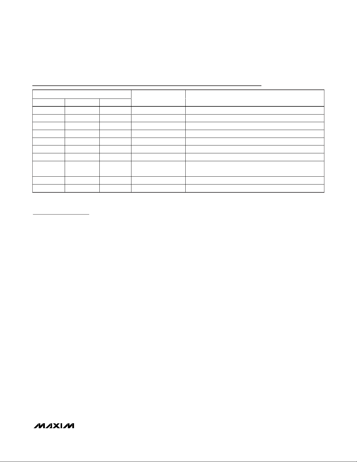
Table 1. Address Selection
A3 A2 A1 A0 ADDRESS
GND GND GND GND 1000 000
GND GND GND V
GND GND V
GND GND V
GND V
GND V
GND V
GND V
V
CC
V
CC
V
CC
V
CC
V
CC
V
CC
V
CC
V
CC
MAX6633
CC
CC
CC
CC
CC
CC
CC
GND GND GND 1001 000
GND GND V
GND V
GND V
V
CC
V
CC
V
CC
V
CC
A2 A1 A0 ADDRESS
GND GND GND 1001 000
GND GND V
GND V
GND V
V
CC
V
CC
V
CC
V
CC
GND GND 1000 100
GND V
V
CC
V
CC
CC
CC
GND GND 1001 100
GND V
V
CC
V
CC
MAX6634
CC
CC
GND GND 1001 100
GND V
V
CC
V
CC
MAX6635
A1 A0 ADDRESS
GND GND 1001 000
GND V
V
CC
V
CC
GND 1000 010
V
CC
CC
GND 1000 110
V
CC
CC
GND 1001 010
V
CC
CC
GND 1001 110
V
CC
CC
GND 1001 010
V
CC
CC
GND 1001 110
V
CC
CC
GND 1001 010
V
CC
1000 001
1000 011
1000 101
1000 111
1001 001
1001 011
1001 101
1001 111
1001 001
1001 011
1001 101
1001 111
1001 001
1001 011

MAX6633/MAX6634/MAX6635
12-Bit Plus Sign Temperature Sensors with
SMBus/I2C-Compatible Serial Interface
______________________________________________________________________________________ 13
Table 2. Pointer Register Bit
Assignments
Table 3. Temperature Register
Table 4. Configuration Register
D15: MSB is the first sign bit.
D2, D1, D0: Flag bits for T
MAX
, T
HIGH
, T
LOW
.
1LSB = 0.0625°C.
Temperature is stored in two’s complement format.
Power-on default = 0h.
D0: 0 = normal operation; 1 = shutdown.
D1: 0 = comparator mode; 1 = interrupt mode.
D2 to D3: 0 = active low; 1 = active high.
D5: 0 = normal SMBus operation; 1 = full I
2
C compatibility.
D7 to D6: Reserved locations, always write zeros.
ADDRESS DESCRIPTION POR STATE
00h
01h
02h T
03h T
04h T
05h T
Temperature register
Configuration-Byte
(READ only)
register
register 0100h
HYST
register 2800h
MAX
register 0500h
LOW
register 2000h
HIGH
0000h
00h
D15 D14 D13 D12 D11 D10 D9 D8 D7 D6 D5 D4 D3 D2 D1 D0
MSB
(Sign)
Bit
12
Bit11Bit
10
Bit 9 Bit 8 Bit 7 Bit 6 Bit 5 Bit 4 Bit 3 Bit 2 Bit 1 T
MAX
T
HIGHTLOW
D7 D6 D5 D4 D3 D2 D1 D0
00
SMB Timeout
Disable
Fault Queue
Enable
ALERT
Polarity
OVERT
Polarity
Comparator
or Interrupt
Shutdown

MAX6633/MAX6634/MAX6635
D6 to D0: Reads all zeros, cannot be written.
1LSB = 1°C.
Power-On Default: T
HIGH
= +64°C (2000h), T
LOW
= +10°C (0500h), T
MAX
= +80°C (2008h), T
HYST
= 2°C (0100h).
12-Bit Plus Sign Temperature Sensors with
SMBus/I2C-Compatible Serial Interface
14 ______________________________________________________________________________________
Table 5. Fault Queue Depth
Table 7. T
HIGH
, T
LOW
, T
MAX
, and T
HYST
Registers
Table 6. Output Code vs. Temperature
D4 NO. OF FAULTS
0 1 (DEFAULT)
14
TEMP. (°C)
+150.0000 0100 1011 0000 0XXX 4B00
+125.0000 0011 1110 1000 0XXX 3E80
+25.0000 0000 1100 1000 0XXX 0C80
+0.0625 0000 0000 0000 1XXX 0008
DIGITAL OUTPUT CODE
BINARY
MSB LSB
HEX
0.0000 0000 0000 0000 0XXX 0000
-0.0625 1111 1111 1111 1XXX FFF8
-25.0000 1111 0011 0111 0XXX F370
-55.0000 1110 0100 0111 0XXX E470
D15 D14 D13 D12 D11 D10 D9 D8 D7 D6 D5 D4 D3 D2 D1 D0
MSB
(Sign)
Bit 7 Bit 6 Bit 5 Bit 4 Bit 3 Bit 2 Bit 1 LSB 0000000

MAX6633/MAX6634/MAX6635
12-Bit Plus Sign Temperature Sensors with
SMBus/I2C-Compatible Serial Interface
______________________________________________________________________________________ 15
Pin Configurations
TOP VIEW
SDA
A3
1
1
2
87V
A0SCL
MAX6633
3
4
A1
6
A2GND
5
SO
SDA
CC
2
MAX6634
3
ALERT
4
SO
87V
6
5
SDA
CC
A0SCL
1
2
87V
CC
A0SCL
MAX6635
A1
OVERT
3
A2GND
GND
4
A1
6
5
ALERT
SO

MAX6633/MAX6634/MAX6635
12-Bit Plus Sign Temperature Sensors with
SMBus/I2C-Compatible Serial Interface
Maxim cannot assume responsibility for use of any circuitry other than circuitry entirely embodied in a Maxim product. No circuit patent licenses are
implied. Maxim reserves the right to change the circuitry and specifications without notice at any time.
16
____________________Maxim Integrated Products, 120 San Gabriel Drive, Sunnyvale, CA 94086 408-737-7600
© 2001 Maxim Integrated Products Printed USA is a registered trademark of Maxim Integrated Products.
Package Information
N
HE
1
TOP VIEW
D
C
L
SIDE VIEW
e
FRONT VIEW
A
B
A1
INCHES
DIM
A1
B
C
e 0.050 BSC 1.27 BSC
E
H 0.2440.228 5.80 6.20
VARIATIONS:
D
D
0∞-8∞
MAX
MIN
0.069
0.053A
0.010
0.004
0.014
0.019
0.007
0.010
0.150
0.157
0.016L
0.050
INCHES
MAX
MINDIM
0.189 0.197 AA5.004.80 8
0.337 0.344 AB8.758.55 14
0.3940.386D
MILLIMETERS
MAX
MIN
1.35
1.75
0.10
0.25
0.35
0.49
0.19
0.25
3.80 4.00
0.40 1.27
MILLIMETERS
MAX
MIN
9.80 10.00
N MS012
16
AC
SOICN .EPS
PROPRIETARY INFORMATION
TITLE:
PACKAGE OUTLINE, .150" SOIC
REV.DOCUMENT CONTROL NO.APPROVAL
21-0041
1
B
1
 Loading...