MAXIM MAX6629 Technical data

General Description
The MAX6629–MAX6632 are local digital temperature
sensors with an SPI™-compatible serial interface. The
temperature is converted to a 12-bit + sign word with a
resolution of 0.0625°C/LSB. An extended temperature
range provides useful readings up to +150°C.
These sensors are 3-wire serial interface SPI compatible, allowing the MAX6629–MAX6632 to be readily connected to a variety of microcontrollers (µCs). The
MAX6629–MAX6632 are read-only devices, simplifying
their use in systems where only temperature data is
required.
All four digital temperature sensors require very little
supply current, making them ideal for portable systems.
The MAX6631/MAX6632 perform a temperature-to-digital conversion once every 8s and require minimal average supply current, 32µA (typ). The MAX6629/
MAX6630 perform a conversion once every 0.5s and
require only 200µA (typ) supply current. Any of these
temperature sensors can perform conversions more
often—up to approximately four conversions per second by reading the conversion results more often.
Applications
Features
♦ Low Power Consumption
32µA typ (MAX6631/MAX6632)
200µA typ (MAX6629/MAX6630)
♦ 12-Bit + Sign Resolution with 0.0625°C/LSB
♦ Accuracy
±1°C (max) from 0°C to +70°C
♦ +150°C Extended Temperature Range
♦ SPI-Compatible Serial Interface
♦ +3.0V to +5.5V Supply Range
♦ 6-Pin TDFN and SOT23 Packages
♦ Lead-Free Version Available (TDFN Package)
MAX6629–MAX6632
12-Bit + Sign Digital Temperature Sensors
with Serial Interface
________________________________________________________________
Maxim Integrated Products
1
Pin Configurations
19-2047; Rev 4; 5/10
Ordering Information
SPI is a trademark of Motorola, Inc.
V
CC
SO
GND
SCK
μC
+3V TO +5.5V
0.1μF
MAX6629
MAX6630
MAX6631
MAX6632
CS
Typical Application Circuit
Cellular
Hard Disk Drive
HVAC
Automotive
Industrial Control
Systems
For pricing, delivery, and ordering information, please contact Maxim Direct at 1-888-629-4642,
or visit Maxim’s website at www.maxim-ic.com.
+
Denotes a lead(Pb)-free/RoHS-compliant package.
*
EP = Exposed pad.
PART TEMP RANGE PIN-PACKAGE
MAX6629MTT+ -55°C to +125°C 6 TDFN-EP*
MAX6629MUT -55°C to +125°C 6 SOT23-6
MAX6630MTT+ -55°C to +125°C 6 TDFN-EP*
MAX6630MUT -55°C to +125°C 6 SOT23-6
MAX6631MTT+ -55°C to +125°C 6 TDFN-EP*
MAX6631MUT -55°C to +125°C 6 SOT23-6
MAX6632MTT+ -55°C to +125°C 6 TDFN-EP*
MAX6632MUT -55°C to +125°C 6 SOT23-6
TOP VIEW
16SO
N.C.
GND
MAX6629
2
MAX6631
34
CC
SOT23
TDFN TDFN
CS
5
SCKV
16SO
GND
N.C.
MAX6630
2
MAX6632
34
CC
SOT23
CS
5
SCKV

MAX6629–MAX6632
12-Bit + Sign Digital Temperature Sensors
with Serial Interface
2 _______________________________________________________________________________________
ABSOLUTE MAXIMUM RATINGS
Stresses beyond those listed under “Absolute Maximum Ratings” may cause permanent damage to the device. These are stress ratings only, and functional
operation of the device at these or any other conditions beyond those indicated in the operational sections of the specifications is not implied. Exposure to
absolute maximum rating conditions for extended periods may affect device reliability.
All Voltages Referenced to GND
V
CC
...........................................................................-0.3V, +6.0V
SO, SCK, CS ....................................................-0.3V, V
CC
+ 0.3V
SO .......................................................................-1mA to +50mA
Current into Any Pin ............................................................10mA
Continuous Power Dissipation (T
A
= +70°C)
6-Pin SOT23 (derate 9.10mW/°C above +70°C)..........727mW
6-Pin TDFN (derate 24.4mW/°C above +70°C) .........1951mW
Junction Temperature......................................................+150°C
Operating Temperature Range (Note 1) ...........-55°C to +150°C
Storage Temperature Range .............................-65°C to +150°C
Lead Temperature (soldering, 10s) .................................+300°C
Soldering Temperature (reflow)
TDFN............................................................................+260°C
SOT23 (Ordering Information contains “#”) .................+245°C
SOT23 (Ordering Information contains “-”)..................+240°C
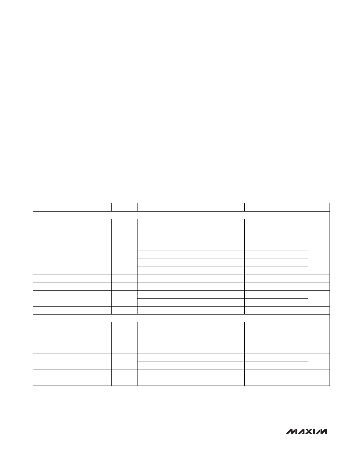
ELECTRICAL CHARACTERISTICS
(VCC= +3.0V to +5.5V, TA= -55°C to +125°C, unless otherwise noted. Typical values are at VCC= +3.3V and TA= +25°C.) (Notes 2
and 3)
Note: It is not recommended to operate the device above +125°C for extended periods of time.
TEMPERATURE
Accuracy
Power-Supply Sensitivity PSS 0.2 0.6 °C/V
Resolution 0.0625 °C
Time Between Conversion
Starts
Conversion Time t
POWER SUPPLY
Supply Voltage Range VCC 3.0 5.5 V
Supply Current, SCK Idle
Average Operating Current I
Power-On Reset (POR)
Threshold
PARAMETER S YMBOL CONDITIONS MIN TYP MAX UNITS
TA = room temp, VCC = +3.3V -0.8 ±0.2 +0.8
0°C TA +70°C, VCC = +3.3V -1.0 ±0.2 +1.0
-20°C TA +85°C, VCC = +3.3V -1.6 +0.3 +1.6
-20°C TA +100°C, VCC = +3.3V -2.3 +0.5 +2.3 °C
-40°C TA +125°C, VCC = +3.3V -3.2 +0.8 +3.2
TA -55°C, VCC = +3.3V -1.0 +1.5 +3.5
= +150°C, VCC = +3.3V -5.0 +1.5 +6.5
T
A
t
SAMPLE
CONV
ISD Shutdown (Note 3), VCC = +0.8V 5
I
IDLE
I
CONV
CC
MAX6629, MAX6630, CS high 0.37 0.5 0.65
MAX6631, MAX6632, CS high 5.9 8 10.5
180 250 320 ms
ADC idle (Figure 2), CS = low 6 20
ADC converting (Figure 2) 360 650
MAX6629, MAX6630 200 400
MAX6631, MAX6632 32 50
V
falling 1.6 V
CC
s
μA
μA

MAX6629–MAX6632
12-Bit + Sign Digital Temperature Sensors
with Serial Interface
_______________________________________________________________________________________ 3
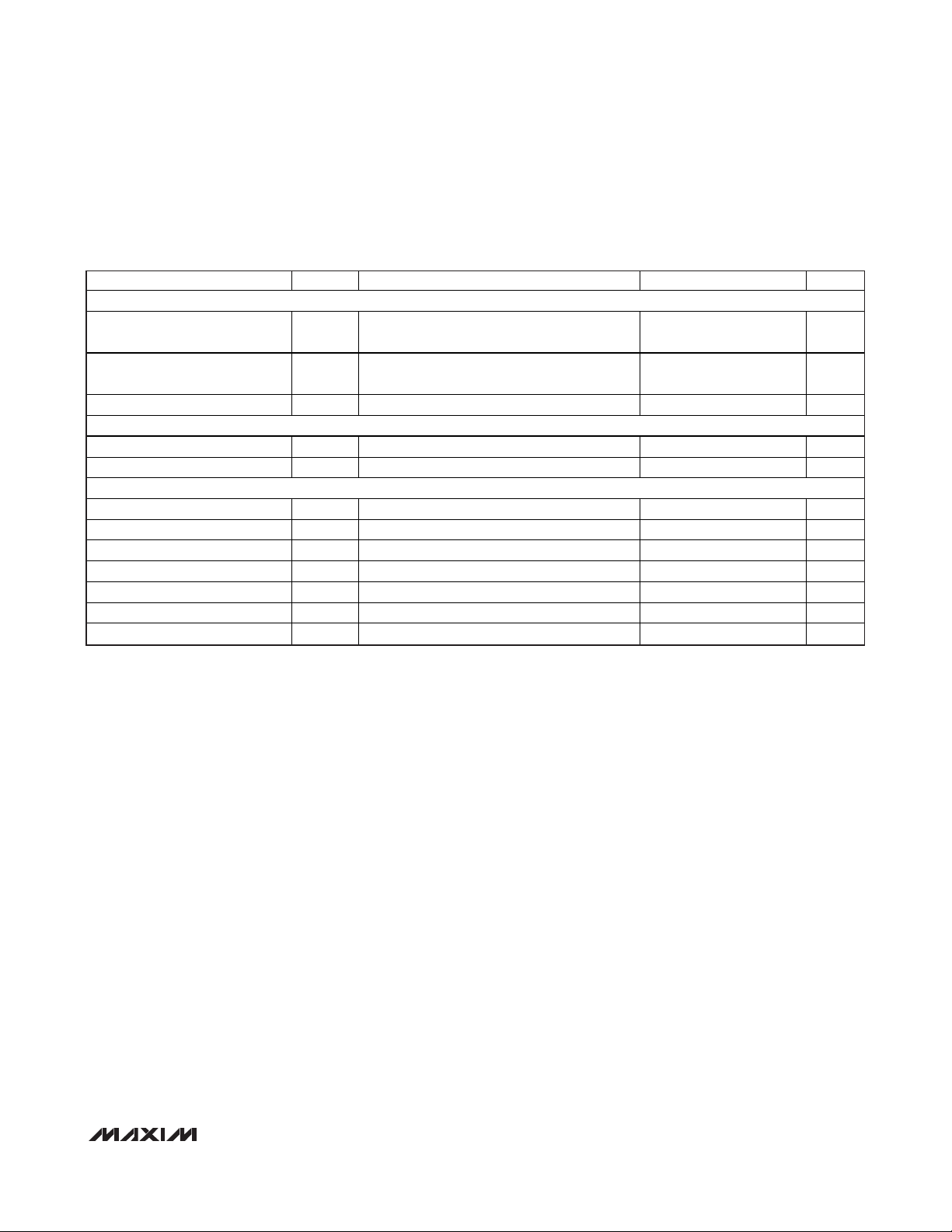
ELECTRICAL CHARACTERISTICS (continued)
(VCC= +3.0V to +5.5V, TA= -55°C to +125°C, unless otherwise noted. Typical values are at VCC= +3.3V and TA= +25°C.) (Notes 2
and 3)
Note 2: Tested at a single temperature. Specifications over temperature are guaranteed by design.
Note 3: The MAX6629–MAX6632 are not specifically equipped with a shutdown function. Their low supply current permits powering
them from the output of a logic gate. This specification is given to ensure that the MAX6629–MAX6632 do not draw
excessive currents at low supply voltages, ensuring reliable operation from a gate output.
Note 4: Timing characteristics are guaranteed by design and are not production tested.
Note 5: C
LOAD
= total capacitance of one bus line in picofarads.
LOGIC INPUTS (CS, SCK)
Logic Input Low Voltage VIL
Logic Input High Voltage V
Input Leakage Current I
LOGIC OUTPUTS (SO)
Output Low Voltage VOL I
Output High Voltage VOH I
TIMING CHARACTERISTICS (Notes 4 and 5)
Serial Clock Frequency f
SCK Pulse Width High tCH 100 ns
SCK Pulse Width Low tCL 100 ns
CS Fall to SCK Rise t
CS Fal l to Output Enable tDV C
CS Ri se to Output Disable tTR C
SCK Fal l to Output Data Valid tDO C
PARAMETER S YMBOL CONDITIONS MIN TYP MAX UNITS
0.3 x
V
CC
IH
VIN = V
LEAK
SINK
SOURCE
5 MHz
SCL
C
CSS
LOAD
LOAD
LOAD
LOAD
or + 5.5V ±1 ±5 μA
GND
= 1.6mA 0.4 V
= 1.6mA VCC - 0.4 V
= 10pF 80 ns
= 10pF 80 ns
= 10pF 50 ns
= 10pF 80 ns
0.7 x
V
V
CC
V
 Loading...