

Page 1
General Description
The MAX6625/MAX6626 combine a temperature sensor,
a programmable overtemperature alarm, and an I2Ccompatible serial interface into single compact packages.
They convert their die temperatures into digital values
using internal analog-to-digital converters (ADCs). The
result of the conversion is held in a temperature register,
readable at any time through the serial interface. A dedicated alarm output, OT, activates if the conversion result
exceeds the value programmed in the high-temperature
register. A programmable fault queue sets the number of
faults that must occur before the alarm activates, preventing spurious alarms in noisy environments. OT has programmable output polarity and operating modes.
The MAX6625/MAX6626 feature a shutdown mode that
saves power by turning off everything but the power-on
reset and the I2C-compatible interface. Four separate
addresses can be configured with the ADD pin, allowing
up to four MAX6625/MAX6626 devices to be placed on
the same bus. The MAX6625P/MAX6626P OT outputs are
open drain, and the MAX6625R/MAX6626R OT outputs
include internal pullup resistors.
The MAX6625 has a 9-bit internal ADC and can function
as a replacement for the LM75 in most applications. The
MAX6626 has a 12-bit internal ADC. Both devices come
in the space-saving 6-pin SOT23 package, or the 6-pin
TDFN package.
Applications
Fan Control
Temperature Alarms
System Temperature Control
Industrial Equipment
Features
♦ 9-Bit Temperature-to-Digital Converter (MAX6625)
♦ 12-Bit Temperature-to-Digital Converter (MAX6626)
♦ I
2
C-Compatible Serial Interface
♦ Up to Four Devices on a Single Bus
♦ Versatile Alarm Output with Programmable Trip
Temperature and Hysteresis
♦ Low-Power Shutdown Mode
♦ Space-Saving TDFN or SOT23 Packages
♦ Lead-Free Version Available (TDFN Package)
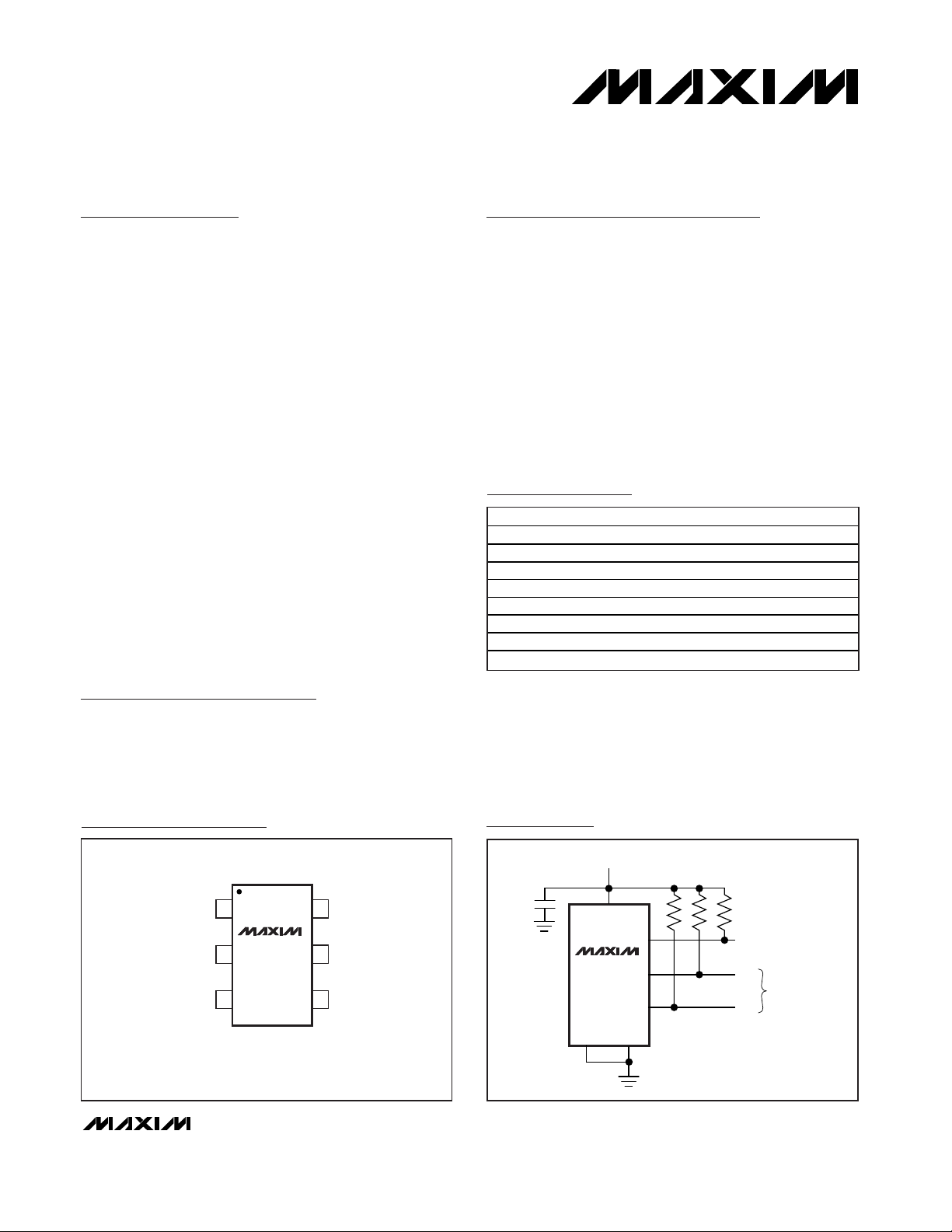
MAX6625/MAX6626
9-Bit/12-Bit Temperature Sensors with
I2C-Compatible Serial Interface in a SOT23
________________________________________________________________ Maxim Integrated Products 1
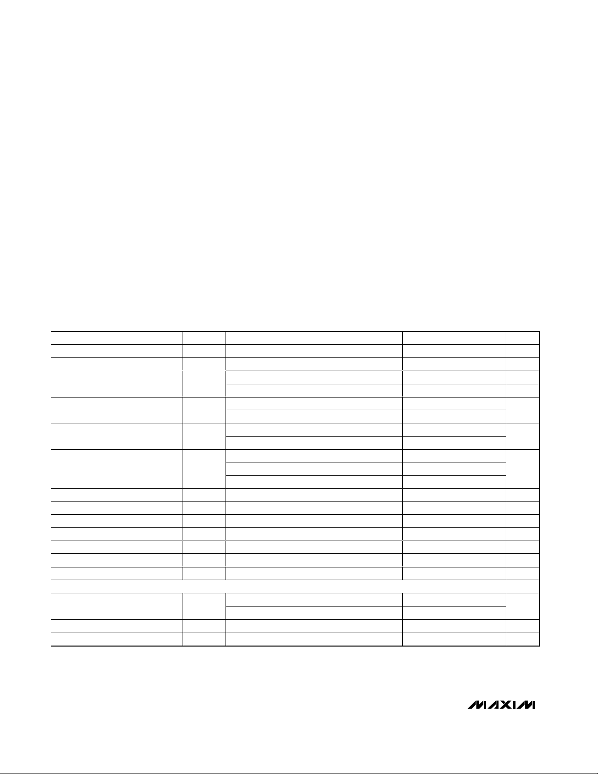
GND
OT
**EP = EXPOSED PADDLE
SCL
16V
S
5 ADD
SDA
MAX6625
MAX6626
SOT236
TDFN-EP**
TOP VIEW
2
34
Pin Configuration
4
6
V
S
0.1µF
1
MAX6625
MAX6626
3
SCL
TO I
2
C
MASTER
10kΩ
(OMIT FOR MAX6625R
AND MAX6626R)
SDA
52
1kΩ
1kΩ
OT OUTPUT
Typical Operating Circuit
19-1841; Rev 4; 10/06
Note: All devices operate over the -55°C to +125°C temperature
range.
*For device options, see Selector Guide at end of data sheet.
Requires special solder temperature profile described in the
Absolute Maximum Ratings section.
**EP = Exposed paddle.
PART PIN-PACKAGE PKG CODE
MAX6625PMUT* 6 SOT23-6 U6F-6
MAX6625RMUT* 6 SOT23-6 U6F-6
MAX6625PMTT* 6 TDFN-EP** T633-1
MAX6625RMTT* 6 TDFN-EP** T633-1
MAX6626PMUT* 6 SOT23-6 U6F-6
MAX6626RMUT* 6 SOT23-6 U6F-6
MAX6626PMTT* 6 TDFN-EP** T633-1
MAX6626RMTT* 6 TDFN-EP** T633-1
For pricing, delivery, and ordering information, please contact Maxim/Dallas Direct! at
1-888-629-4642, or visit Maxim’s website at www.maxim-ic.com.
Ordering Information
Page 2
MAX6625/MAX6626
9-Bit/12-Bit Temperature Sensors with
I2C-Compatible Serial Interface in a SOT23
2 _______________________________________________________________________________________
ABSOLUTE MAXIMUM RATINGS
ELECTRICAL CHARACTERISTICS
(+3V ≤ VS≤ +5.5V, T
A =
-55°C to +125°C, unless otherwise noted.)
Stresses beyond those listed under “Absolute Maximum Ratings” may cause permanent damage to the device. These are stress ratings only, and functional
operation of the device at these or any other conditions beyond those indicated in the operational sections of the specifications is not implied. Exposure to
absolute maximum rating conditions for extended periods may affect device reliability.
VSto GND ................................................................-0.3V to +6V
OT, SCL, SDA to GND..............................................-0.3V to +6V
ADD to GND .................................................-0.3V to (V
S
+ 0.3V)
Current into Any Pin............................................................±5mA
OT Sink Current.................................................................. 20mA
Continuous Power Dissipation
6-Pin SOT23 (derate 9.1mW/°C above +70°C)............727mW
6-Pin TDFN (derate 23.8mW/°C above +70°C) .........1905mW
Junction Temperature......................................................+150°C
Storage Temperature Range .............................-60°C to +150°C
ESD Rating (Human Body Model)......................................2000V
Lead Temperature .............................................................Note 1
Note 1: This device is constructed using a unique set of packaging techniques that impose a limit on the thermal profile the device
can be exposed to during board-level solder attach and rework. This limit permits only the use of the solder profiles recommended in the industry-standard specification, IPC/JEDEC J-STD-020A, paragraph 7.6, Table 3 for IR/VPR and Convection
Reflow. Preheating is required. Hand or wave soldering is not allowed.
PARAMETER
SYMBOL
CONDITIONS
MIN
TYP
MAX
UNITS
Power-Supply Voltage V
S
3.0 5.5 V
I2C-compatible active 1 mA
I2C-compatible inactive
µAQuiescent Current I
C
Shutdown mode 1 µA
MAX6625 9
ADC Resolution
MAX6626 12
MAX6625 0.5
Temperature Resolution
MAX6626
TA = +25°C, VS = +3V to +3.6V ±1
0°C = TA ≤ +50°C, VS = +3.0V to +3.6V
Accuracy (Notes 2, 3)
0°C = T
A
≤ +70°C, VS = +3.0V to +3.6V
°C
Power-Supply Sensitivity VS = +3V to +5.5V 1
Conversion Time t
C
ms
OT Pullup Resistor R
P
MAX6625R, MAX6626R only 25 50 kΩ
OT Saturation Voltage (Note 4) V
L
I
OUT
= 4mA (Note 4) 0.8 V
OT Delay (Programmable through fault queue)
ms
T
HIGH
Default Temperature
80 °C
T
LOW
Default Temperature T
LOW
75 °C
I2C-COMPATIBLE I/O: SCL, SDA, ADD
VS < +3.6V 2
Input High Voltage V
IH
VS > +3.6V 3
V
Input Low Voltage V
IL
0.8 V
Input Hysteresis 0.2 V
250
0.0625
T
HIGH
133
1 × t
C
±1.5
±2.0
6 × t
Bits
°C/LSB
°C/V
C
Page 3
MAX6625/MAX6626
9-Bit/12-Bit Temperature Sensors with
I2C-Compatible Serial Interface in a SOT23
_______________________________________________________________________________________ 3
ELECTRICAL CHARACTERISTICS (continued)
(+3V ≤ VS≤ +5.5V, T
A =
-55°C to +125°C, unless otherwise noted.)
Note 2: Guaranteed by design and characterization to ±5 sigma.
Note 3: Quantization error not included in specifications for temperature accuracy.
Note 4: Output current should be minimized for best temperature accuracy. Power dissipation within the MAX6625/MAX6626 causes
self-heating and temperature drift; see the Thermal Considerations section.
Note 5: A master device must provide a hold time of at least 300ns for the SDA signal in order to bridge the undefined region of
SCL’s falling edge.
Note 6: C
B
= total capacitance of one bus line in pF. Tested with CB= 400pF.
Note 7: Input filters on SDA, SCL, and ADD suppress noise spikes less than 50ns.
PARAMETER
SYMBOL
CONDITIONS
MIN
TYP
MAX
UNITS
Input High Leakage Current I
IH
V
IN
= +5V ±1 µA
Input Low Leakage Current I
IL
V
IN
= 0 ±1 µA
Input Capacitance C
IN
10 pF
Output Low Voltage V
OL
I
OL
= 3mA 0.4 V
Output High Current I
OH
VOH = 5V 1 µA
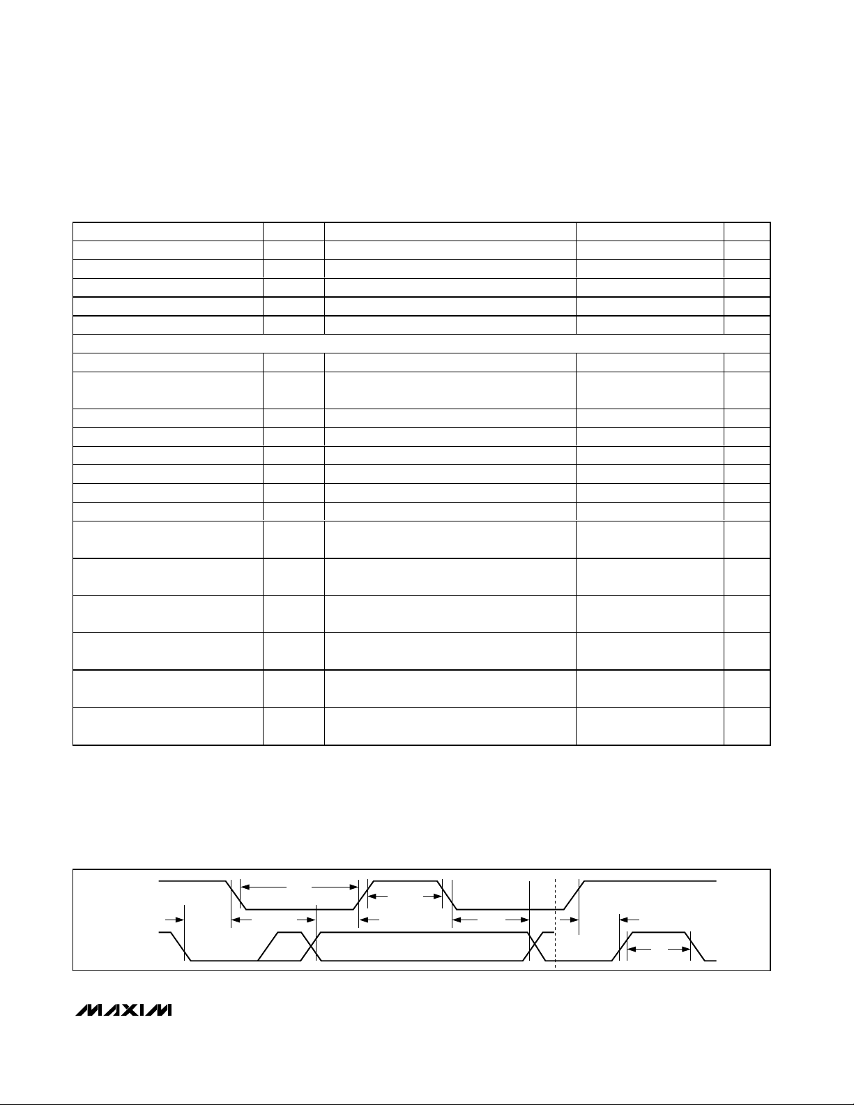
I2C-COMPATIBLE TIMING
Serial Clock Frequency f
SCL
DC
kHz
Bus Free Time Between STOP
and START Conditions
t
BUF
1.3 µs
START Condition Hold Time
0.6 µs
STOP Condition Setup Time
0.6 µs
Clock Low Period t
LOW
1.3 µs
Clock High Period t
HIGH
0.6 µs
Data Setup Time
ns
Data Hold Time
(Note 5) 0 0.9 µs
Maximum Receive SCL/SDA
Rise Time
t
R
(Note 6)
ns
Minimum Receive SCL/SDA
Rise Time
t
R
(Note 6)
20 +
ns
Maximum Receive SCL/SDA
Fall Time
t
F
(Note 6)
ns
Minimum Receive SCL/SDA
Fall Time
t
F
(Note 6)
20 +
ns
Transmit SDA Fall Time t
F
CB = 400pF, IO = 3mA (Note 6)
20 +
ns
Pulse Width of Suppressed
Spike
t
SP
(Note 7) 50 ns
Figure 1. Serial Bus Timing
SCL
SDA
t
F
t
LOW
t
SU:DAT
t
HD:STA
t
HD:DAT
t
SU:STO
t
BUF
t
HIGH
t
R
t
HD:STA
t
SU:STO
t
SU:DAT
t
HD:DAT
100
300
0.1C
300
0.1C
0.1C
B
400
B
B
250
Page 4
MAX6625/MAX6626
9-Bit/12-Bit Temperature Sensors with
I2C-Compatible Serial Interface in a SOT23
4 _______________________________________________________________________________________
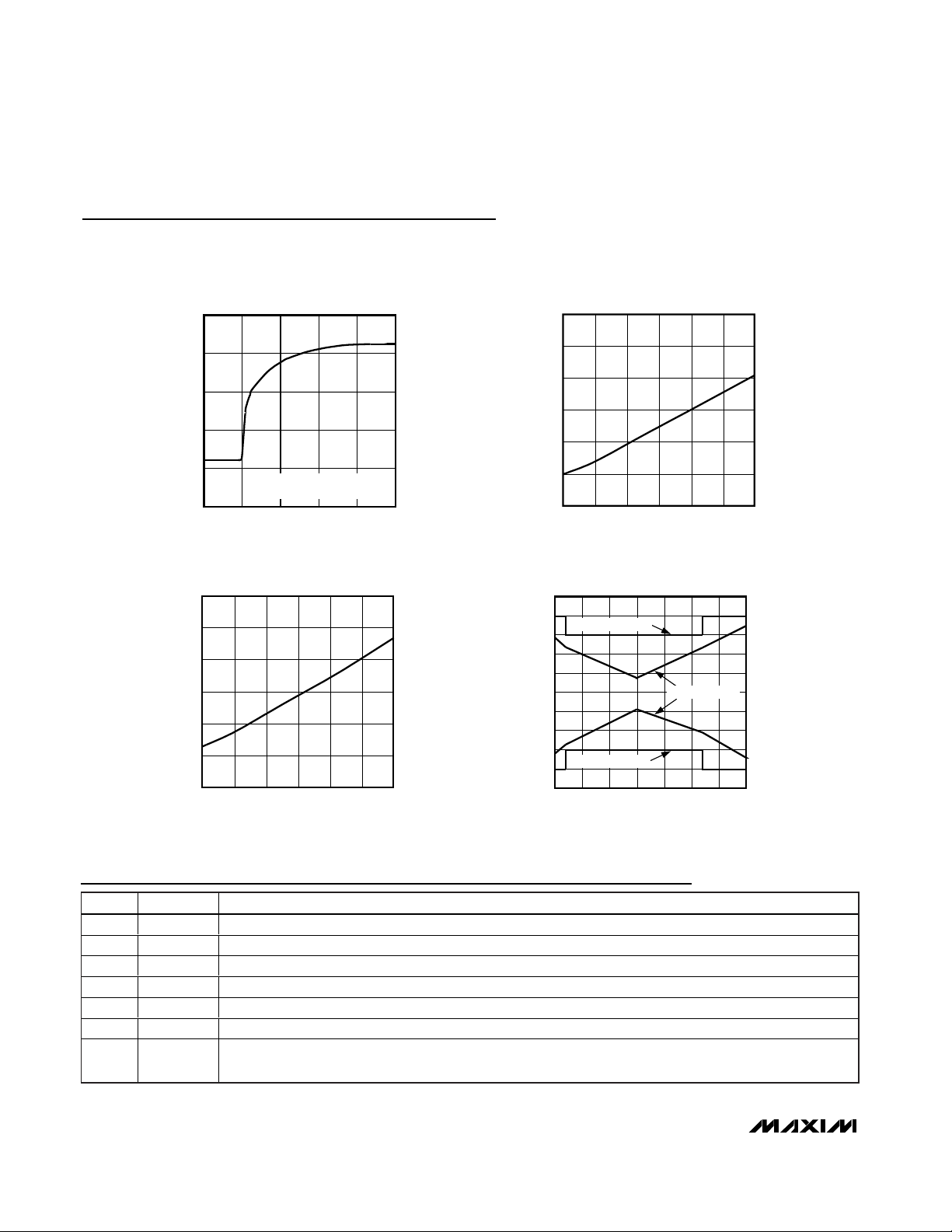
Typical Operating Characteristics
(VS = +3.3V, TA = +25°C, unless otherwise noted.)
Pin Description
0
20
60
40
80
100
-5 50101520
RESPONSE TO THERMAL SHOCK
TEMPERATURE vs. TIME
MAX6625 toc01
TIME (s)
OUTPUT TEMPERATURE (°C)
DEVICE IMMERSED IN +85°C
FLUORINERT BATH
80
120
100
160
140
180
200
-55 5 35-25 65 95 125
STATIC QUIESCENT SUPPLY CURRENT
vs. TEMPERATURE
MAX6625 toc02
TEMPERATURE (°C)
INPUT CURRENT (µA)
80
120
100
160
140
180
200
-55 5 35-25 65 95 125
DYNAMIC QUIESCENT SUPPLY CURRENT
vs. TEMPERATURE
MAX6625 toc03
TEMPERATURE (°C)
INPUT CURRENT (µA)
-5
-2
-3
-4
0
-1
4
3
2
1
5
-50 -25 0 25 50 75 100 125
TEMPERATURE ERROR
vs. TEMPERATURE
MAX6625 toc04
TEMPERATURE (°C)
TEMPERATURE ERROR (°C)
MAXIMUM LIMIT
±5 SIGMA RANGE
MINIMUM LIMIT
PIN NAME FUNCTION
1 SDA I2C-Compatible Serial Bidirectional Data Line
2 GND Power-Supply Ground
3 SCL I2C-Compatible Clock Input
4 OT Temperature Alarm Output
5 ADD I2C-Compatible Address Set Pin: Ground (0), VS (1), SDA (2), SCL (3); see Table 1.
6VSPower-Supply Input, +3V to +5.5V. Bypass VS to GND with a 0.1µF capacitor.
—EP
Exposed Paddle. Internally connected to GND. Connect to a large ground plane for maximum thermal
dissipation.
Page 5
MAX6625/MAX6626
9-Bit/12-Bit Temperature Sensors with
I2C-Compatible Serial Interface in a SOT23
_______________________________________________________________________________________ 5
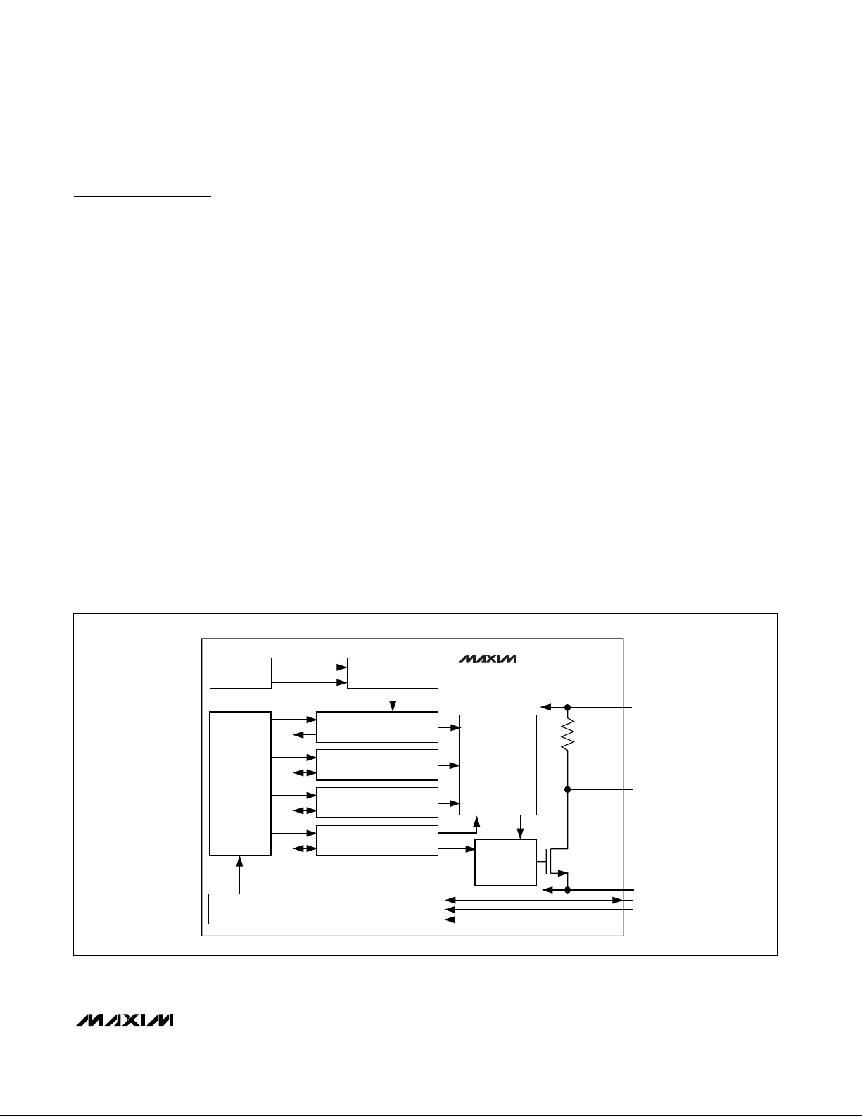
Detailed Description
The MAX6625/MAX6626 continuously convert their die
temperatures into digital values using their self-contained delta-sigma ADCs. The resulting data is readable at any time through the I2C-compatible serial
interface. A dedicated alarm output asserts if the result
exceeds the value in the programmable high-temperature register. A programmable fault queue sets the
number of faults that must occur before the alarm
asserts, preventing spurious alarms in noisy environments. The alarm output polarity is selectable and
deasserts based on either of two operating modes,
comparator or interrupt. In comparator mode, the OT
output deasserts if the temperature conversion result
falls below the programmable low-temperature register
value (subject to the fault queue conditions) providing
adjustable hysteresis. In interrupt mode, the OT output
deasserts when any register is read through the serial
interface. Each conversion cycle takes about 130ms. At
power-up, the temperature register is set to 8000H until
the first conversion is completed.
The MAX6625/MAX6626 feature a shutdown mode,
accessible through the serial interface, that saves power
by turning off everything but the power-on reset and the
I2C-compatible interface. While in shutdown mode, the
temperature register is set to 8000H. The device func-
tions as a slave on the I
2
C-compatible bus supporting
Write Byte, Write Word, Read Byte, and Read Word commands. Four separate addresses can be configured with
the ADD pin, allowing up to four MAX6625/MAX6626
devices to be placed on the same bus. Figure 2 shows
the functional diagram of the MAX6625/MAX6626.
Serial interface
I2C-Compatible Operation
The MAX6625/MAX6626 are readable and programmable through their I2C-compatible serial interface.
Figures 3 and 4 show the timing details of the clock
(SCL) and data (SDA) signals. The device functions as
a slave on the I2C-compatible bus and supports Write
Byte, Write Word, Read Byte, and Read Word commands.
Addressing
Four separate addresses can be configured with the
ADD pin, allowing up to four MAX6625/MAX6626s to be
placed on the same bus. The address is selected by
connecting the ADD pin to either of four places: GND
(address 0), VS(address 1), SDA (address 2), or SCL
(address 3). Table 1 shows the full I2C-compatible
address for each state.
MAX6625
MAX6626
TEMPERATURE REGISTER
T
HIGH
REGISTER
+Vs
OT
GND
SDA
SCL
ADD
SERIAL BUS INTERFACE
T
LOW
REGISTER
SET-POINT
COMPARATOR
ADDRESS
POINTER
REGISTER
BANDGAP
REGISTER
ADC
REFERENCE
TEMP SIGNAL
FAULT
QUEUE
COUNTER
CONFIGURATION REGISTER
MAX665_ R
ONLY
Figure 2. Functional Diagram
Page 6
MAX6625/MAX6626
9-Bit/12-Bit Temperature Sensors with
I2C-Compatible Serial Interface in a SOT23
6 _______________________________________________________________________________________
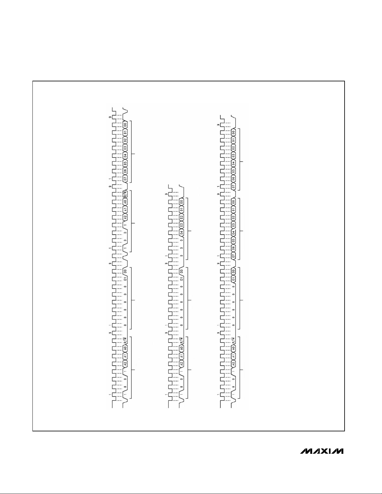
Figure 3. I2C-Compatible Timing Diagram
ADDRESS
BYTE
ADDRESS
BYTE
ADDRESS
BYTE
(a) TYPICAL POINTER SET FOLLOWED BY IMMEDIATE READ FROM CONFIGURATION REGISTER
(b) CONFIGURATION REGISTER WRITE
(c) T
HIGH
AND T
LOW
WRITE
POINTER
BYTE
POINTER
BYTE
POINTER
BYTE
MOST-SIGNIFICANT
DATA BYTE
LEAST-SIGNIFICANT
DATA BYTE
CONFIGURATION
BYTE
ADDRESS
BYTE
DATA
BYTE
ACK BY
MAX6625
ACK BY
MAX6625
ACK BY
MAX6625
ACK BY
MAX6625
ACK BY
MAX6625
ACK BY
MAX6625
ACK BY
MAX6625
START
BY
MASTER
START
BY
MASTER
START
BY
MASTER
REPEAT
START
BY
MASTER
NO
ACK BY
MASTER
STOP
COND BY
MASTER
ACK BY
MAX6625
ACK BY
MAX6625
STOP
COND BY
MASTER
STOP
COND BY
MASTER
ACK BY
MAX6625
Page 7

MAX6625/MAX6626
9-Bit/12-Bit Temperature Sensors with
I2C-Compatible Serial Interface in a SOT23
_______________________________________________________________________________________ 7
Figure 4. I2C-Compatible Timing Diagram
ADDRESS
BYTE
ADDRESS BYTE
ADDRESS
BYTE
ADDRESS
BYTE
DATA
BYTE
(a) TYPICAL 2-BYTE READ FROM PRESET POINTER LOCATION SUCH AS TEMP, T
HIGH
, T
LOW
(b) TYPICAL POINTER SET FOLLOWED BY IMMEDIATE READ FOR 2-BYTE REGISTER SUCH AS TEMP, T
HIGH
, T
LOW
(c) TYPICAL 1-BYTE READ FROM CONFIGURATION REGISTER WITH PRESET POINTER
MOST-SIGNIFICANT
DATA BYTE
LEAST-SIGNIFICANT
DATA BYTE
POINTER BYTE
MOST-SIGNIFICANT
DATA BYTE
LEAST-SIGNIFICANT
DATA BYTE
ACK BY
MAX6625
ACK BY
MASTER
ACK BY
MAX6625
ACK BY
MAX6625
ACK BY
MASTER
ACK BY
MAX6625
ACK BY
MASTER
START
BY
MASTER
START
BY
MASTER
REPEAT
START
BY
MASTER
START
BY
MASTER
STOP
COND BY
MASTER
STOP
COND BY
MASTER
STOP
COND BY
MASTER
NO ACK BY
MASTER
NO
ACK BY
MASTER
NO
ACK BY
MASTER
Page 8

MAX6625/MAX6626
9-Bit/12-Bit Temperature Sensors with
I2C-Compatible Serial Interface in a SOT23
8 _______________________________________________________________________________________
Control Registers
Five registers control the operation of the MAX6625/
MAX6626 (Figure 5 and Tables 2 through 7). The pointer register should be the first addressed and determines which of the other four registers are acted on.
The other four are the temperature, configuration, hightemperature (T
HIGH
), and low-temperature (T
LOW
) registers. The temperature register is 9 bits for the
MAX6625 and 12 bits for the MAX6626, read only, and
contains the latest temperature data. The register
length is 16 bits with the unused bits masked to zero.
The digital temperature data contained in the temperature register is in °C, using a two’s-complement format
with 1 LSB corresponding to 0.5°C for the MAX6625
and 0.0625°C for the MAX6626 (Table 8).
The configuration register is 8 bits, read/write, and contains the fault queue depth, the temperature alarm
polarity select bit, the interrupt mode select bit, and the
shutdown control bit. The high-temperature register is
9 bits, read/write, and contains the value that triggers
the overtemperature alarm. The low-temperature register is 9 bits, read/write, and contains the value to which
the temperature must fall before the overtemperature
alarm is deasserted, if in comparator mode.
Temperature Conversion
An on-chip bandgap reference produces a signal proportional to absolute temperature (PTAT), as well as the
temperature-stable reference voltage necessary for the
analog-to-digital conversion. The PTAT signal is digitized by the on-board ADC to a resolution of 0.5°C for
the MAX6625, and 0.0625°C for the MAX6626. The
resulting digital value is placed in the temperature register. The temperature conversion runs continuously
and asynchronously from the I
2
C-compatible interface
at a rate of 133ms per conversion. When the temperature register is read, the most recently completed conversion result is provided and the currently active
conversion is aborted. When the bus transaction is finished by an I2C-compatible stop condition conversions
resume.
Overtemperature Alarm
The dedicated overtemperature output pin, OT, has
programmable polarity and two modes: comparator
and interrupt. Polarity and mode are selected through
the configuration register, and alarm activity is governed by a fault queue. Fault queue depth is also
selected through the configuration register (Tables 5
and 6). The MAX6625P/MAX6626P OT output is open
POINTER REGISTER
(SELECTS REGISTER FOR
COMMUNICATION)
INTERFACE
SDA
SCL
DATA
ADDRESS
REGISTER SELECT
CONFIGURATION
(READ-WRITE, SETS OPERATING MODES)
POINTER = 00000001
T
LOW
SET-POINT
(READ-WRITE)
POINTER = 00000010
TEMPERATURE
(READ ONLY)
POINTER = 00000000
T
HIGH
SET-POINT
(READ-WRITE)
POINTER = 00000011
Figure 5. MAX6625/MAX6626 Programmers Model
ADD CONNECTION
I2C-COMPATIBLE ADDRESS
GND 100 1000
V
S
100 1001
SDA 100 1010
SCL 100 1011
Table 1. Address Selection
Page 9

MAX6625/MAX6626
9-Bit/12-Bit Temperature Sensors with
I2C-Compatible Serial Interface in a SOT23
_______________________________________________________________________________________ 9
D7
D2 D1 D0
0
0
Register select
(see Table 3)
Table 2. Pointer Register
D7 to D2: Read all zeros, cannot be written.
PART D15
D14
D13
D12
D11
D10D9D8D7D6D5D4D3D2–D0
MAX6625
0000 0
MAX6625
MSB
Bit
Bit
0
Table 4. Temperature Register
D7
D2 D1 D0
0
Fault
OT
Mode
Shutdown
Table 5. Configuration Register
All defaults = 0.
D0: 0 = Normal operation, 1 = Shutdown.
D1: 0 = Comparator mode, 1 = Interrupt mode.
D2: 0 = Active low, 1 = Active high.
D7 to D5: Reserved locations, always write zeros.
D4 D3 NO. OF FAULTS
0 0 1 (default)
01 2
10 4
11 6
Table 6. Fault Queue Depth
D1 D0 REGISTER
0 0 Temperature (default)
0 1 Configuration
10T
LOW
11T
HIGH
Table 3. Register Select
D6 to D0, MAX6625: Read all zeros, cannot be written.
D2 to D0, MAX6626: Read all zeros, cannot be written.
D15: MSB is the sign bit.
1 LSB = 0.5°C for the MAX6625.
1 LSB = 0.0.0625°C for the MAX6626.
Temperature is stored in two’s-complement format.
D6 D5 D4 D3
0000
MSB
(Sign)
(Sign)
Bit 7 Bit 6 Bit 5 Bit 4 Bit 3 Bit 2 Bit 1 LSB
11
10
Bit 9 Bit 8 Bit 7 Bit 6 Bit 5 Bit 4 Bit 3 Bit 2 Bit 1 LSB
D6 D5 D4 D3
Comparator
00
Queue
Depth
Polarity
or Interrupt
Page 10

MAX6625/MAX6626
9-Bit/12-Bit Temperature Sensors with
I2C-Compatible Serial Interface in a SOT23
10 ______________________________________________________________________________________
D15
D14
D13
D12
D11
D10D9D8D7D6D5D4D3D2D1D0
MSB
0000000
Table 7. T
HIGH
and T
LOW
Registers
D6 to D0: Read all zeros, cannot be written.
D15: MSB is the sign bit.
Default: T
HIGH
= +80°C (5000H), T
LOW
= +75°C (4B00H).
LSB = 0.5°C.
DIGITAL OUTPUT CODE
MAX6625 MAX6626
BINARY BINARY
TEMPERATURE
(°C)
MSB LSB
HEX
MSB LSB
HEX
+125.0000 0111 1101 0000 0000 7D00 0111 1101 0000 0000 7D00
+124.9375 0111 1100 1000 0000 7C80 0111 1100 1111 0000 7CF0
+25.0000 0001 1001 0000 0000 1900 0001 1001 0000 0000 1900
+0.5000 0000 0000 1000 0000 0080 0000 0000 1000 0000 0080
0.0000 0000 0000 0000 0000 0000 0000 0000 0000 0000 0000
-0.5000 1111 1111 1000 0000 FF80 1111 1111 1000 0000 FF80
-25.0000 1110 0111 0000 0000 E700 1110 0111 0000 0000 E700
-55.0000 1100 1001 0000 0000 C900 1100 1001 0000 0000 C900
∗ 1000 0000 0000 0000 8000 1000 0000 0000 0000 8000
Table 8. Output Code vs. Temperature
*8000H is the default value at power-up and after coming out of shutdown.
Bit 7 Bit 6 Bit 5 Bit 4 Bit 3 Bit 2 Bit 1 LSB
Page 11

MAX6625/MAX6626
9-Bit/12-Bit Temperature Sensors with
I2C-Compatible Serial Interface in a SOT23
______________________________________________________________________________________ 11
drain, and the MAX6625R/MAX6626R output includes
an internal 35kΩ (typ) pullup resistor. Figure 6 shows
the OT alarm operation and reset details.
Fault Queue
A programmable fault queue on the MAX6625/
MAX6626 eliminates spurious alarm activity in noisy
environments. The queue sets the number of consecutive out-of-tolerance temperature readings that must
occur before the OT alarm output is toggled. An out-oftolerance reading is above T
HIGH
or below T
LOW
. The
fault queue depth defaults to one at power-up and may
be programmed to one, two, four, or six consecutive
conversions. Any time the conversion result is in tolerance, and OT is not asserted, the queue is cleared,
even if it contains some out-of-tolerance counts.
Additionally, the fault queue automatically clears at
power-up, in shutdown, or if a master writes to any of
the T
HIGH
, T
LOW
, or configuration registers. Whenever
the fault queue is cleared, OT is deasserted.
For example, the fault queue is set to four, two consecutive out-of-tolerance readings have occurred, and the
master writes to the T
LOW
register. The fault queue is
cleared and begins to look for four new consecutive
out-of-tolerance conversions.
Comparator Mode
In comparator mode, OT is asserted when the number
of consecutive conversions exceeding the value in the
T
HIGH
register is equal to the depth of the fault queue.
OT deasserts when the number of consecutive conversions less than the value in the T
LOW
register is equal
to the depth of the fault queue. T
HIGH
minus T
LOW
is
the effective hysteresis of the OT output.
For example, if T
HIGH
is set to +100°C, T
LOW
is set to
+80°C, and the fault queue depth is set to four, OT
does not assert until four consecutive conversions
exceed +100°C. Then, OT does not deassert until four
consecutive conversions are less than +80°C.
Comparator mode allows autonomous clearing of an OT
fault without the intervention of a master and is ideal to
use for driving a cooling fan (Figure 7).
Interrupt Mode
In interrupt mode, the MAX6625/MAX6626 look for a
T
HIGH
or a T
LOW
fault based on previous fault activity.
The OT pin asserts an alarm for an undertemperature
fault, as well as for an overtemperature fault, depending
on certain conditions. If the fault queue is cleared at
power-up, the IC looks for a T
HIGH
fault. After a T
HIGH
fault, the IC looks for a T
LOW
fault. After a T
LOW
fault,
the IC looks for a T
HIGH
fault, and it bounces back and
forth if properly deasserted each time. Once either fault
has occurred, it remains active indefinitely until
deasserted by a read of any register, and the device
then begins to look for a fault of the opposite type. Also,
if the fault queue is cleared, OT is deasserted and the
IC once again looks for a T
HIGH
fault. The activation of
any fault is subject to the depth of the fault queue.
DIE
TEMPERATURE
TIME
** *
T
HIGH
T
LOW
OT
(COMPARATOR MODE)
OT
(INTERRUPT MODE)
TEMPERATURE RESPONSE
SHOWN WITH OT SET FOR
ACTIVE LOW
*THIS ASSUMES DEASSERTION OF OT BY A
MASTER THROUGH THE SERIAL INTERFACE.
SEE INTERRUPT MODE SECTION.
Figure 6. OT Alarm Output and Reset Diagram
Page 12

MAX6625/MAX6626
9-Bit/12-Bit Temperature Sensors with
I2C-Compatible Serial Interface in a SOT23
12 ______________________________________________________________________________________
Example 1: If T
HIGH
is set to +100°C, T
LOW
is set to
+80°C, and the fault queue depth is set to four, OT
does not assert until four consecutive conversions
exceed +100°C. If the temperature is then read through
the I2C-compatible interface, OT deasserts. OT asserts
again when four consecutive conversions are less than
+80°C.
Example 2: If T
HIGH
is set to +100°C, T
LOW
is set to
+80°C, and the fault queue depth is set to four, OT
does not assert until four consecutive conversions
exceed +100°C. If the T
HIGH
register is then changed
to +120°C, OT deasserts and the IC looks for a new
T
HIGH
fault.
Shutdown
The MAX6625/MAX6626 offer a low-power shutdown
mode. Enter shutdown mode by programming the shutdown bit of the control register high. In shutdown, the
temperature register is set to 8000H and the ADC is
turned off, reducing the device current draw to 1µA
(typ). After coming out of shutdown, the temperature
register continues to read 8000H until the first conversion result appears. The fault queue is held in reset
during shutdown.
Thermal Considerations
The MAX6625/MAX6626 supply current is less than
1mA when the I2C-compatible interface is active. When
used to drive high-impedance loads, the devices dissipate negligible power; therefore, the die temperature is
essentially the same as the package temperature. The
key to accurate temperature monitoring is good thermal
contact between the MAX6625/MAX6626 package and
the monitored device or circuit. In some applications,
the 6-pin SOT23 package may be small enough to fit
underneath a socketed µP, allowing the device to monitor the µP’s temperature directly. Heat flows in and out
of plastic packages primarily through the leads. Short,
wide copper traces leading to the temperature monitor
ensure that heat transfers quickly and reliably. The rise
in die temperature due to self-heating is given by the
following formula:
∆T
J
= P
D
✕
θ
JA
where PDis the power dissipated by the MAX6625/
MAX6626, and θJAis the package’s thermal resistance.
The typical thermal resistance is +110°C/W for the 6pin SOT23 package. To limit the effects of self-heating,
minimize the output currents. For example, if the
MAX6625/MAX6626 sink 4mA with the maximum OT V
L
specification of 0.8V, an additional 3.2mW of power is
dissipated within the IC. This corresponds to a 0.35°C
rise in the die temperature.
Applications
Figure 7 shows the MAX6625/MAX6626 used as a temperature-triggered fan controller. Figure 8 shows the
MAX6625/MAX6626 used as a thermostat to control a
heating element.
4
6
+V
S
+3V TO +5V
+12V
OT
MAX6625R
MAX6626R
2
12V 300mA
FAN MOTOR
LOGIC LEVEL
MOSFET
Figure 7. Fan Controller
Figure 8. Simple Thermostat
+V
S
+3V TO +5V
6
4k
MAX6625P
MAX6626P
3
5
OT
2N3904
HEATER
RELAY
5VDC, 20mA
125VAC, 1A
HEATER
SUPPLY
Page 13

MAX6625/MAX6626
9-Bit/12-Bit Temperature Sensors with
I2C-Compatible Serial Interface in a SOT23
______________________________________________________________________________________ 13
TRANSISTOR COUNT: 7513
PROCESS: BiCMOS
Chip Information
PART
ALARM
OUTPUT
(bits)
M A X 6 62 5P Open drain 9
MAX6625R
9
M A X 6 62 6P Open drain 12
MAX6626R
12
Selector Guide
Internal pullup
Internal pullup
RESOLUTION
TOP
MARK
AAHY
AAHZ
AANP
AANQ
Page 14

MAX6625/MAX6626
9-Bit/12-Bit Temperature Sensors with
I2C-Compatible Serial Interface in a SOT23
14 ______________________________________________________________________________________
6LSOT.EPS
Package Information
(The package drawing(s) in this data sheet may not reflect the most current specifications. For the latest package outline information,
go to www.maxim-ic.com/packages
.)
Page 15

MAX6625/MAX6626
9-Bit/12-Bit Temperature Sensors with
I2C-Compatible Serial Interface in a SOT23
______________________________________________________________________________________ 15
Package Information (continued)
(The package drawing(s) in this data sheet may not reflect the most current specifications. For the latest package outline information,
go to www.maxim-ic.com/packages
.)
Page 16

MAX6625/MAX6626
9-Bit/12-Bit Temperature Sensors with
I2C-Compatible Serial Interface in a SOT23
16 ______________________________________________________________________________________
6, 8, &10L, DFN THIN.EPS
H
1
2
21-0137
PACKAGE OUTLINE, 6,8,10 & 14L,
TDFN, EXPOSED PAD, 3x3x0.80 mm
Package Information (continued)
(The package drawing(s) in this data sheet may not reflect the most current specifications. For the latest package outline information,
go to www.maxim-ic.com/packages
.)
Page 17

9-Bit/12-Bit Temperature Sensors with
I2C-Compatible Serial Interface in a SOT23
MAX6625/MAX6626
Maxim cannot assume responsibility for use of any circuitry other than circuitry entirely embodied in a Maxim product. No circuit patent licenses are
implied. Maxim reserves the right to change the circuitry and specifications without notice at any time.
Maxim Integrated Products, 120 San Gabriel Drive, Sunnyvale, CA 94086 408-737-7600 ____________________ 17
© 2006 Maxim Integrated Products is a registered trademark of Maxim Integrated Products, Inc.
Package Information (continued)
(The package drawing(s) in this data sheet may not reflect the most current specifications. For the latest package outline information,
go to www.maxim-ic.com/packages
.)
COMMON DIMENSIONS
SYMBOL
MIN. MAX.
A 0.70 0.80
D 2.90 3.10
E 2.90 3.10
A1
0.00 0.05
L 0.20 0.40
PKG. CODE N D2 E2 e JEDEC SPEC b [(N/2)-1] x e
PACKAGE VARIATIONS
0.25 MIN.k
A2 0.20 REF.
2.30±0.101.50±0.106T633-1 0.95 BSC MO229 / WEEA 1.90 REF0.40±0.05
1.95 REF0.30±0.050.65 BSC2.30±0.108T833-1
2.00 REF0.25±0.050.50 BSC2.30±0.1010T1033-1
2.40 REF0.20±0.05- - - - 0.40 BSC1.70±0.10 2.30±0.1014T1433-1
1.50±0.10
1.50±0.10
MO229 / WEEC
MO229 / WEED-3
0.40 BSC - - - - 0.20±0.05 2.40 REFT1433-2 14 2.30±0.101.70±0.10
T633-2 6 1.50±0.10 2.30±0.10
0.95 BSC MO229 / WEEA
0.40±0.05 1.90 REF
T833-2 8 1.50±0.10 2.30±0.10 0.65 BSC MO229 / WEEC 0.30±0.05 1.95 REF
T833-3 8 1.50±0.10 2.30±0.10 0.65 BSC MO229 / WEEC 0.30±0.05 1.95 REF
-DRAWING NOT TO SCALE-
H
2
2
21-0137
PACKAGE OUTLINE, 6,8,10 & 14L,
TDFN, EXPOSED PAD, 3x3x0.80 mm
2.30±0.10
MO229 / WEED-3
2.00 REF0.25±0.05
0.50 BSC
1.50±0.1010T1033-2
Revision History
Pages changed at Rev 4: 1, 2, 15, 16, 17
 Loading...