

Page 1
General Description
The MAX6621 PECI-to-I2C translator provides an efficient, low-cost solution for PECI-to-SMBus
TM
/I2C protocol conversion. The PECI-compliant host reads
temperature data directly from up to four PECI-enabled
CPUs. Interrupts are generated when the measured
temperature exceeds the high-temperature limit and
causes ALERT to assert. The RESET input allows the
host to reset the I2C bus in the event of a communication error.
The I2C interface provides an independent serial communication channel to communicate synchronously with
peripheral devices in a multiple master or multiple slave
system. This interface allows a maximum serial-data
rate of 400kbps.
The MAX6621 is designed to operate from a +3.0V to
+3.6V supply voltage and ambient temperature range
of -20°C to +120°C.
Applications
Servers
Workstations
Desktop Computers
Features
♦ 400kbps I2C-Compatible, 2-Wire Serial Interface
♦ +3V to +3.6V Supply Voltage
♦ PECI-Compliant Port
♦ PECI-to-I
2
C Translation
♦ ALERT Output
♦ RESET Input (May Be Disabled as a Factory
Option)
♦ Programmable Temperature Offsets
♦ -20°C to +120°C Operating Temperature Range
♦ V
REF
Input Refers Logic Levels to the PECI
Supply Voltage
♦ Automatic I2C Bus Lockup Timeout Reset
♦ Lead-Free, 10-Pin µMAX®Package
MAX6621
PECI-to-I2C Translator
________________________________________________________________
Maxim Integrated Products
1
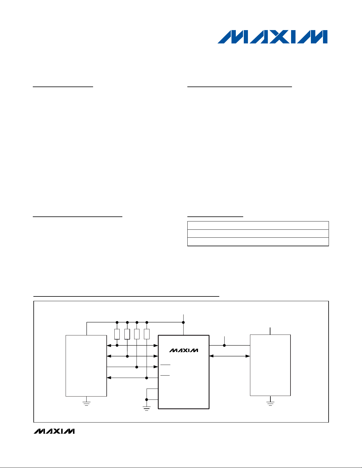
Typical Application Circuit
19-0729; Rev 0; 1/07
For pricing, delivery, and ordering information, please contact Maxim/Dallas Direct! at
1-888-629-4642, or visit Maxim’s website at www.maxim-ic.com.
Pin Configuration appears at end of data sheet.
Ordering Information
T
= Tape-and-reel package.
+
Denotes a lead-free package.
SMBus is a trademark of Intel Corp.
µMAX is a registered trademark of Maxim Integrated Products, Inc.
PART TEMP RANGE PIN-PACKAGE
MAX6621AUB+ -20°C to +120°C 10 µMAX
MAX6621AUB+T -20°C to +120°C 10 µMAX
SDA
SCL
I2C
MASTER
SDA
SCL
RESET
ALERT
AD0
GND
+3.3V
V
CPU
V
V
CC
MAX6621
V
REF
PECI
TT
CPU
INTERNAL
TEMP
SENSOR
Page 2

MAX6621
PECI-to-I2C Translator
2 _______________________________________________________________________________________
ABSOLUTE MAXIMUM RATINGS
ELECTRICAL CHARACTERISTICS
(
Typical Application Circuit
, VCC= +3V to +3.6V, V
REF
= +0.95V to +1.26V, TA= -20°C to +120°C, unless otherwise noted. Typical
values are at V
CC
= +3.3V, V
REF
= +1.0V, TA= +25°C.) (Note 1)
Stresses beyond those listed under “Absolute Maximum Ratings” may cause permanent damage to the device. These are stress ratings only, and functional
operation of the device at these or any other conditions beyond those indicated in the operational sections of the specifications is not implied. Exposure to
absolute maximum rating conditions for extended periods may affect device reliability.
(All voltages with respect to GND.)
V
CC
..........................................................................-0.3V to +4V
AD0, RESET, ALERT...................................-0.3V to (V
CC
+ 0.3V)
SCL, SDA .................................................................-0.3V to +6V
V
REF
.........................................................................-0.3V to +4V
PECI .........................................................-0.3V to (V
REF
+ 0.3V)
DC Current through SDA ...................................................10mA
Continuous Power Dissipation (T
A
= +70°C)
10-Pin µMAX (derate 5.6mW/°C over T
A
= +70°C)......444mW
Operating Temperature Range .........................-20°C to +120°C
Junction Temperature......................................................+150°C
Storage Temperature Range .............................-65°C to +150°C
Lead Temperature (soldering, 10s) .................................+300°C
PARAMETER SYMBOL CONDITIONS MIN TYP MAX UNITS
SUPPLY
Operating Supply Voltage V
Operating Supply Current I
Power-On-Reset Voltage V
INPUT SCL, INPUT/OUTPUT SDA
Low-Level Input Voltage V
High-Level Input Voltage V
Low-Level Output Voltage V
Leakage Current I
Input Capacitance C
ALERT
Low-Level Output Voltage V
ADDRESS INPUT A0/RST
Low-Level Input Voltage V
High-Level Input Voltage V
Leakage Current I
Input Capacitance C
PECI
Supply Voltage to PECI Cell V
Input Voltage Range V
Low-Level Input Voltage
Threshold
High-Level Input Voltage
Threshold
CC
CC
POR
REF
V
V
SCL = 400kHz 4 7 mA
IL
IH
IOL = 6mA 0.4 V
OL
L
I
IOL = 6mA 0.4 V
OL
IL
IH
L
I
IN
IL
IH
x V
x V
0.275
x V
0.550
x V
3.0 3.6 V
2.60 2.95 V
0.3
x V
CC
0.7
CC
5.5 V
-1 +1 µA
10 pF
0.3
x V
CC
0.7
CC
V
CC
+ 0.3
-2 +2 µA
10 pF
0.95 1.26 V
V
-0.3
REF
+ 0.3
0.500
REF
x V
REF
0.725
REF
x V
REF
V
V
V
V
V
V
Page 3

MAX6621
PECI-to-I2C Translator
_______________________________________________________________________________________ 3
ELECTRICAL CHARACTERISTICS (continued)
(
Typical Application Circuit
, VCC= +3V to +3.6V, V
REF
= +0.95V to +1.26V, TA= -20°C to +120°C, unless otherwise noted. Typical
values are at V
CC
= +3.3V, V
REF
= +1.0V, TA= +25°C.) (Note 1)
TIMING CHARACTERISTICS
(
Typical Application Circuit
, VCC= +3V to +3.6V, V
REF
= +0.95V to +1.26V, TA= -20°C to +120°C, unless otherwise noted. Typical
values are at V
CC
= +3.3V, V
REF
= +1.0V, TA= +25°C.) (Note 2)
PARAMETER SYMBOL CONDITIONS MIN TYP MAX UNITS
Hysteresis V
Low-Level Sinking Current I
High-Level Sourcing Current I
Input Capacitance C
Signal-Noise Immunity Above
300MHz
H
IL
IH
(Note 2) 10 pF
I
V
(Note 2)
N
0.1
x V
REF
0.5 1.0 mA
-6 mA
0.1
x V
REF
PARAMETER SYMBOL CONDITIONS MIN TYP MAX UNITS
RESET Pulse Width RST 100 ns
I2C INTERFACE
Serial-Clock Frequency f
Bus Free Time Between a
STOP and a START Condition
Hold Time, (Repeated) START
Condition
Repeated START Condition
Setup Time
STOP Condition Setup Time t
Data Hold Time t
Data Setup Time t
SCL Clock-Low Period t
SCL Clock-High Period t
Rise Time of Both SDA and
SCL Signals, Receiving
Fall Time of Both SDA and
SCL Signals, Receiving
Fall Time of SDA Transmitting t
Pulse Width of Spike
Suppressed
Capacitive Load for Each
Bus Line
PECI INTERFACE
Bit Time (Note 7) t
SCL
t
BUF
t
HD, STA
t
SU, STA
SU, STO
HD, DAT
SU, DAT
LOW
HIGH
t
F.TX
t
C
BIT
(Note 3) 0.9 µs
(Notes 4, 5)
R
t
(Notes 4, 5)
F
(Notes 4, 5)
(Note 6) 50 160 ns
SP
(Note 4) 400 pF
b
Overall time evident on PECI 0.495 500
Driven by MAX6621 0.495 250
400 kHz
1.3 µs
0.6 µs
0.6 µs
0.6 µs
120 ns
1.3 µs
0.6 µs
20
+ 0.1C
20
+ 0.1C
20
+ 0.1C
b
b
b
300 ns
300 ns
250 ns
V
V
P-P
µs
Page 4

MAX6621
PECI-to-I2C Translator
4 _______________________________________________________________________________________
Note 1: All parameters are tested at TA= +25°C. Specifications over temperature are guaranteed by design.
Note 2: Guaranteed by design; not production tested.
Note 3: A master device must provide a hold time of at least 300ns for the SDA signal (referred to V
IL
of the SCL signal) to bridge
the undefined region of SCL’s falling edge.
Note 4: C
b
= total capacitance of one bus line in pF. tRand tFmeasured between 0.3 x VCCand 0.7 x VCC.
Note 5: I
SINK
≤ 6mA. Cb= total capacitance of one bus line in pF. tRand tFmeasured between 0.3 x VCCand 0.7 x VCC.
Note 6: Input filters on the SDA and SCL inputs suppress noise spikes less than 50ns.
Note 7: The MAX6621 must drive a more restrictive time to allow for quantized sampling errors by a client yet still attain the mini-
mum time less than 500µs. t
BIT
limits apply equally to t
BIT-A
and t
BIT-M
.
Note 8: The minimum and maximum bit times are relative to t
BIT
defined in the timing negotiation pulse.
Note 9: Extended trace lengths can appear as additional nodes.
Note 10: The client may deassert its low idle drive prior to the falling edge of the first bit of the message by using the rising edge to
detect a message start. However, the time delay must be sufficient to qualify the rising edge as a true message rather than
a noise spike.
Note 11: The message stop is defined by two consecutive periods when the bus has no rising edge. Tolerance around this time is
based on the t
BIT-M
error budget.
Note 12: t
SETUP
is not additive with t
STOP
. Rather, these times may overlap.
TIMING CHARACTERISTICS (continued)
(
Typical Application Circuit
, VCC= +3V to +3.6V, V
REF
= +0.95V to +1.26V, TA= -20°C to +120°C, unless otherwise noted. Typical
values are at V
CC
= +3.3V, V
REF
= +1.0V, TA= +25°C.) (Note 2)
PARAMETER SYMBOL CONDITIONS MIN TYP MAX UNITS
Bit Time Jitter t
Between adjacent bits in an PECI message
BIT, jitter
header or data bytes after timing has been
negotiated
1%
Change in Bit Time t
High-Level Time for Logic-High t
High-Level Time for Logic-Low t
Client Asserts PECI High
During Logic-High
Rise Time t
Fall Time t
Hold Time t
Stop Time t
Maximum Dwell Time of the
PECI Client
Minimum PECI Low Time
Preceding a Message
BIT, drift
t
SU
HOLD
STOP
t
RESET
t
SETUP
Across a PECI address or PECI message
bits as driven by MAX6621
(Note 8) 0.6 0.75 0.8 x t
H1
H0
0.2 0.3 0.4 x t
2%
0 0.2 x t
Measured from VOL to VPMAX,
R
V
REF(nom)
Measured from VOH to VNMAX,
F
V
REF(nom)
-5% (Note 9)
+5% (Note 9)
Time for client to maintain a low idle drive
after MAX6621 begins a message (Note 10)
A constant low level driven by MAX6621
(Notes 8, 11)
2x t
From the end of a ResetDevice command
to the next message to which the reset
client must be able to respond
If the prior t
the maximum t
t
SETUP
is not known by MAX6621,
BIT
must be assumed and
BIT
= 1ms in this case (Note 12)
2x t
30 +
5/Node
30/Node ns
0.5 x t
0.4 ms
BIT
BIT
BIT-M
ns
BIT-1
BIT-M
BIT-X
Page 5
MAX6621
Pin Description
PECI-to-I2C Translator
_______________________________________________________________________________________ 5
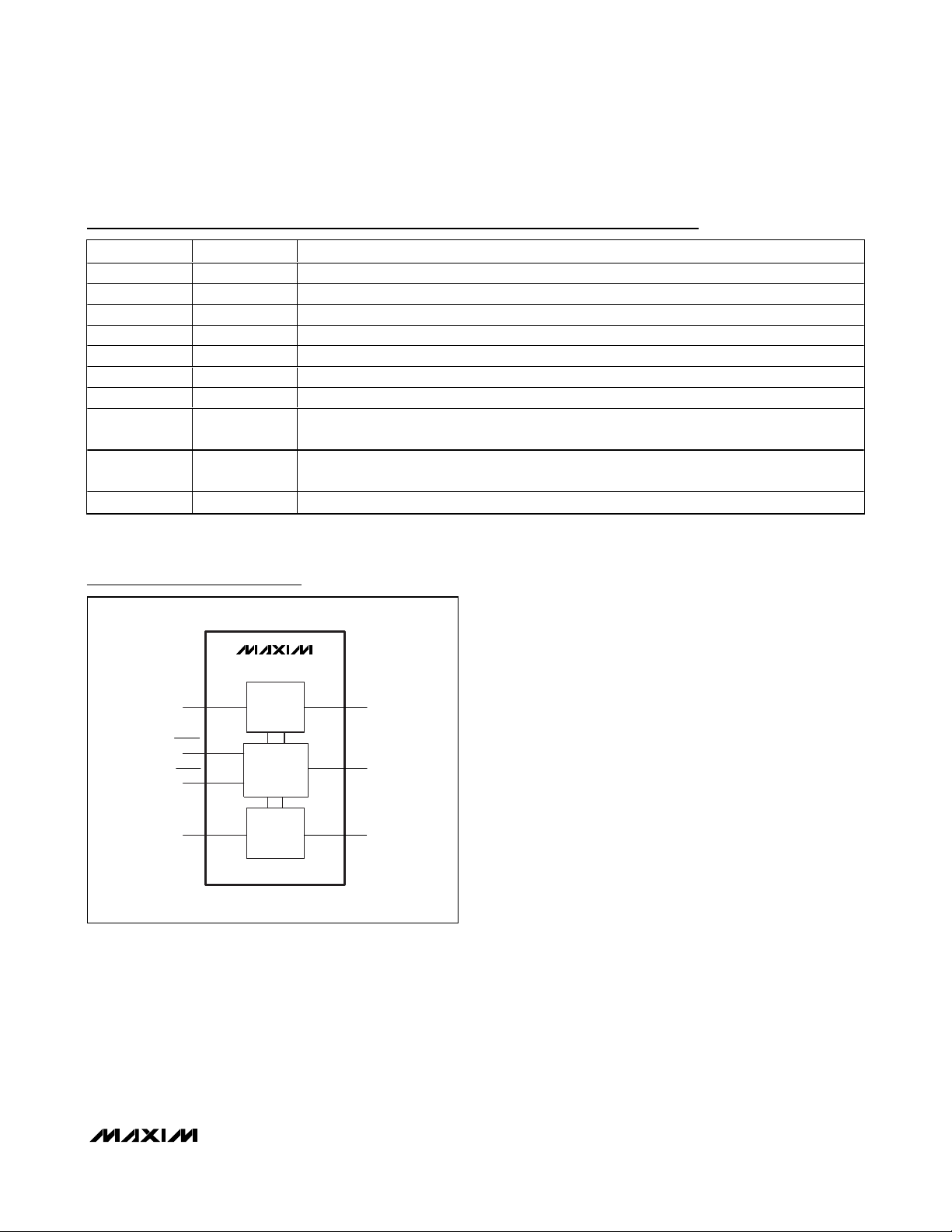
Block Diagram
PIN NAME FUNCTION
1 PECI Platform Environment Control Interface (PECI) Serial-Bus Input/Output
2 AGND Analog Ground
3 AD0 I2C Bus Device Address Selection Input
4 SDA I2C Bus Data Input/Output
5 SCL I2C Bus Clock Input/Output
6VCCPower Supply. Bypass to GND with a 0.1µF capacitor.
7 GND Power-Supply Ground
2
I
8 RESET
9 ALERT
10 V
REF
C Reset Input. Pull RESET low to reset I2C interface and default all registers to startup values.
Drive high for normal operation.
ALERT Interrupt Open-Drain Output. Asserts low when any temperature exceeds the
programmed limit.
PECI Input Supply Voltage. Bypass V
to AGND with a 0.1µF capacitor.
REF
MAX6621
SDA
RESET
ALERT
PECI
2
C
I
PORT
PECI
TRANSLATION
ENGINE
PECI
PORT
SCL
A0
V
REF
Page 6

MAX6621
PECI-to-I2C Translator
6 _______________________________________________________________________________________
Configuration
The MAX6621 has four configuration registers (Table 1).
CONFIG0 is the main configuration register that enables
the PECI sockets, I2C bus timeout, PEC, alert activation,
and polling delay. CONFIG1 sets the number of retries,
CONFIG2 sets the temperature offset, and CONFIG3
controls the temperature averaging. You can write to
the configuration registers to set the configuration or
read from the configuration registers to get the current
settings.
Detailed Description
The MAX6621 obtains temperature data from an internal temperature sensor in PECI-compliant hosts. Up to
four PECI hosts can be connected to the PECI I/O interface. The MAX6621 handles all the PECI transmissions
and uses a 2-wire, I
2
C-compatible serial interface to
communicate with the PECI host.
Registers and Commands
The following is an overview of the I2C/SMBus registers/commands supported by the MAX6621.
Table 1. Configuration Registers
ADDRESS DESCRIPTION TRANSACTION TYPE
00h Read socket 0, domain 0 temperature register ReadWord
01h Read socket 0, domain 1 temperature register ReadWord
02h Read socket 1, domain 0 temperature register ReadWord
03h Read socket 1, domain 1 temperature register ReadWord
04h Read socket 2, domain 0 temperature register ReadWord
05h Read socket 2, domain 1 temperature register ReadWord
06h Read socket 3, domain 0 temperature register ReadWord
07h Read socket 3, domain 1 temperature register ReadWord
08h Read maximum temperature for all enabled sockets/domains register ReadWord
09h Read firmware version register ReadWord
0Ah Read maximum temperature address ReadWord
0Bh Read socket and domain that caused alert ReadWord
0Ch Read/write CONFIG0 register ReadWord/WriteWord
0Dh Read/write CONFIG1 register ReadWord/WriteWord
0Eh Read/write CONFIG2 register ReadWord/WriteWord
0Fh Read/write CONFIG3 register ReadWord/WriteWord
10h Read/write alert temperature for socket 0 ReadWord/WriteWord
11h Read/write alert temperature for socket 1 ReadWord/WriteWord
12h Read/write alert temperature for socket 2 ReadWord/WriteWord
13h Read/write alert temperature for socket 3 ReadWord/WriteWord
14h Request polling SendByte
15h Clear alert SendByte
COMMAND BYTE REGISTER DESCRIPTION TYPE RESULT
0Ch CONFIG0 register ReadWord/WriteWord See the CONFIG0 section.
0Dh CONFIG1 register ReadWord/WriteWord See the CONFIG1 section.
0Eh CONFIG2 register ReadWord/WriteWord See the CONFIG2 section.
0Fh CONFIG3 register ReadWord/WriteWord See the CONFIG3 section.
Page 7

CONFIG0
The CONFIG0 register holds a bit mask for sockets and
domains that are enabled for polling as well as a
polling delay (minimum delay between sets of polls)
and features enable/disable bits. Table 2 shows the
various options for CONFIG0.
The optional polling delay (bits 2:0) inserts after polling
the set of all sockets and domains that are enabled in
bits 15:8 with a minimal pause of 2.5ms between PECI
reads. After polling all enabled sockets and domains,
the device pauses PECI communications for the configured time before starting to poll the set of enabled
sockets and domains again. Table 3 shows the various
polling delay options.
CONFIG1
The CONFIG1 register configures the maximum number of retries before aborting a PECI temperature read
as well as the originated (suggested) PECI bit time.
Table 4 shows the various options for CONFIG1.
MAX6621
PECI-to-I2C Translator
_______________________________________________________________________________________ 7
Table 2. CONFIG0 Register
Table 3. Polling Delay
Table 4. CONFIG1 Register
BIT(S) DESCRIPTION DEFAULT
15:8 Polling enable for sockets and domains 00h
15 1 = enable socket 3, domain 1 0
14 1 = enable socket 3, domain 0 0
13 1 = enable socket 2, domain 1 0
12 1 = enable socket 2, domain 0 0
11 1 = enable socket 1, domain 1 0
10 1 = enable socket 1, domain 0 0
9 1 = enable socket 0, domain 1 0
8 1 = enable socket 0, domain 0 0
1 = enable I
7
0 = disable timeout
1 = alternate data representation
6
0 = 16-bit data representation
1 = enable I
(PEC) on device return data
5
0 = disable PEC
1 = mask temperature alerts
4
0 = activate alerts
3 Reserved, set to 0 0
2:0 Poll delay, see Table 3 5
2
C bus lockup timeout
2
C packet error checksum
1
0
1
0
POLL DELAY VALUE DELAY BETWEEN POLLS (ms)
0 Polling on request only
1 2.5
25
310
450
5 100 (default)
6 500
7 Reserved
BIT(S) DESCRIPTION DEFAULT
Originated PECI bit time
(before negotiation)
15:8
7:0
01h: RESERVED
02h…0FFh: CONFIG1[15:8] + 1µs
Minimum: 02h (= 3µs / 333.3kHz)
Maximum: 0FFh (= 256µs / 3.906kHz)
Maximum number of retries for PECI
transactions
02h
03h
Page 8

MAX6621
PECI-to-I2C Translator
8 _______________________________________________________________________________________
CONFIG2
The CONFIG2 register holds the offset that is added to
all temperature return values that are not error codes.
The offset is enabled in CONFIG0, bit 6; +95°C is set
as 17C0h or 005Fh, depending on the data format. To
represent +95°C in 16-bit representation, convert
+95°C to binary using two’s complement and left-shift
six times. The MAX6621 automatically converts the offset value to the equivalent value when the data format
is changed. See Table 5 for the default offset and Table
6 for some example values.
When configured in CONFIG2, and the return code is not
an error code (see the
Error Codes
section), the device
adds the offset value stored in CONFIG2 to the return
value. For example, if the CPU’s thermal control circuit
activation point is at +95°C, CONFIG2 can be set to
+95°C (005Fh or 17C0h) and all return values are converted to absolute temperatures. Note that the thermal
control circuit activation point is CPU specific. The offset
value is represented in the current data format.
CONFIG3
CONFIG3 register configures the temperature averaging
function. See the
Temperature Averaging
section for
more information. Table 7 shows the default settings.
Temperature Representation
Temperature data is formatted in 16-bit two’s complement representing a range from -512°C to +512°C in
steps of 1/64°C (Figure 1). Internally, the device always
uses the 16-bit data format. The temperature is given in
two’s complement and left-shifted so that the +1°C bit
is bit 6 (Figure 2). Temperatures can be represented
externally in alternate data format if fractional readings
are not needed. Table 8 shows some examples.
Table 5. CONFIG2 Register
Table 6. Example Offset Values in 16-Bit
Temperature Representation
Table 7. CONFIG3 Register
Figure 1. Temperature Measured in 1/64°C Steps
Figure 2. Conversion of Temperature Done in Two’s
Complement
Table 8. Example 16-Bit Representation
with No Offset (Activation Point = +95°C)
BIT(S) DESCRIPTION DEFAULT
15:0 Temperature offset 0000h
TEMP (°C) HEX
0 0000h 0000 0000 0000 0000
+25 0640h 0000 0110 0100 0000
+50 0C80h 0000 1100 1000 0000
+75 12C0h 0001 0010 1100 0000
+95 17C0h 0001 0111 1100 0000
BINARY
RESHI RESLO
1
°C °C °C
2
RESLO
1°C
TWO'S
-50°C
COMPLEMENT
1
8
1
°C °C °C
4
00110111
1
32
1
16
01234567
1
64
RESHI
89101112131415
RESLO
BIT(S) DESCRIPTION DEFAULT
15:8 Reserved, set to 0 00h
7:0 Averaging shift count, see formula 00h
TEMP
(°C)
+94 -1 FFC0h 1111 1111 1100 0000
+85 -10 FD80h 1111 1101 1000 0000
+70 -25 FDC0h 1111 1101 1100 0000
+45 -50 F380h 1111 0011 1000 0000
+20 -75 ED30h 1110 1101 0100 0000
RELATIVE
TEMP (°C)
HEX
01234567
BINARY
RESHI RESLO
Page 9

MAX6621
PECI-to-I2C Translator
_______________________________________________________________________________________ 9
Alternate Temperature Value Representation
This optional feature can be enabled using bit 6 of
CONFIG0. When the alternate data format is enabled, the
temperature value is shifted right as shown in Table 9.
The most significant bits are set to all 0s or all 1s depending on the sign bit 15, also shown as S in Figure 3. Table
10 shows some example values. This translation is not
performed for error codes (16-bit values from 8000h
through 81FFh).
Excluding error codes, the software only has to examine the RESLO data byte, as it represents an integer
value in the range from -128°C to +127°C in 1°C steps.
The RESHI byte is all 0s or all 1s for valid return codes,
and either 80h or 81h for all error codes.
Temperature Averaging
The MAX6621 can average several temperature readings and return a value as calculated by:
where T
OLD
is the previously stored temperature, T
PECI
is the new value read from PECI, and T
NEW
is the newly
stored temperature ready to be returned through I
2
C.
This calculation can cause significant bits to be lost.
Enable temperature averaging by writing the desired
averaging amount to the CONFIG3 register. Writing 00h
to the CONFIG3 register disables temperature averaging.
Figure 3. Alternate Temperature Representation
Table 9. Alternate Temperature
Representation
Table 10. Example Alternate Representation with No Offset (Activation Point = +95°C)
DESCRIPTION RESHI RESLO
16-bit value 15:14:13:12:11:10:9:8 7:6:5:4:3:2:1:0
Alternate
representation
15:15:15:15:15:15:15:15 15:12:11:10:9:8:7:6
TxT xT
NEW
1
=+−
2
33
CONFIG
PECI
⎛
1
⎜
⎝
CONFIG
2
1
⎞
⎟
⎠
OLD
RESHI
S X X 12 11 10 9 8
S S S S S S S S S 12 11 10 9 8 7 6
RESLO
7 6 X X X X X X
INTEGER VALUE (~ 1°C)(SIGN BITS)
FRACTIONAL VALUE
TEMP (°C) RELATIVE TEMP (°C) HEX
+94 -1 FFFFh 1111 1111 1111 1111
+85 -10 FFF6h 1111 1111 1111 0110
+70 -25 FFE7h 1111 1111 1110 0111
+45 -50 FFCEh 1111 1111 1100 1110
+20 -75 FFB5h 1111 1111 1011 0101
RESHI RESLO
BINARY
Page 10

MAX6621
PECI-to-I2C Translator
10 ______________________________________________________________________________________
Temperature Commands
Table 11 shows the different commands for selecting
one of the PECI hosts or getting the maximum temperature. Read commands are initiated by the MAX6621,
and the result returned is a 16-bit word with the least
significant bit (LSB) clocked in first for the selected
PECI host.
The result consists of RESLO for the 8 LSBs and RESHI
for the 8 MSBs, resulting in a 16-bit word. The 16-bit
words are temperature values read from the PECI interface. PECI-enabled Intel microprocessors return temperature data in fractions of 1°C below the
thermal-control-circuit activation point, resulting in negative return values that do not represent absolute temperatures. Absolute temperatures can be achieved by
setting the temperature offset in CONFIG2.
Table 12 shows example return values for an Intel CPU.
Note that the MAX6621 does not interpret the return
Table 11. Read Temperature
Table 12. Return Temperature Values
ADDRESS REGISTER TYPE RESULT
00h Socket 0, domain 0
01h Socket 0, domain 1
02h Socket 1, domain 0
03h Socket 1, domain 1
04h Socket 2, domain 0
05h Socket 2, domain 1
06h Socket 3, domain 0
07h Socket 3, domain 1
08h
Read maximum temperature for all enabled
sockets/domains
ReadWord 16-bit words
RELATIVE
TEMPERATURE (°C)
-1
-36
-37
-38
-39
-40
-41
-42
-43
16 BITS ALTERNATE 16 BITS ALTERNATE
0000 0000 FFC0 FFFF
17C0 005F 1780 005E
0000 0000 F700 FFDC
17C0 005F 0ec0 003B
0000 0000 F6C0 FFDB
17C0 005F 0E80 003A
0000 0000 F680 FFDA
17C0 005F 0E40 0039
0000 0000 F640 FFD9
17C0 005F 0E00 0038
0000 0000 F600 FFD8
17C0 005F 0DC0 0037
0000 0000 F5C0 FFD7
17C0 005F 0D80 0036
0000 0000 F580 FFD6
17C0 005F 0D40 0035
0000 0000 F540 FFD5
17C0 005F 0D00 0034
CONFIG2 RESHI:RESLO
Page 11

MAX6621
PECI-to-I2C Translator
______________________________________________________________________________________ 11
data (with the exception of error codes) and the relative
temperatures are listed for reference only. Table 12
shows the values with 16-bit and alternate word format.
The read maximum temperature command from Table 11
returns the highest temperature that is not an error
code from the enabled PECI sockets and domains. This
operation works on signed numbers only and does not
give information as to what socket the temperature
result comes from. To find the socket and domain, use
the read maximum temperature address command as
shown in Table 13.
The read maximum temperature address command
returns the register that had the highest temperature
when read maximum temperature was last called. An
error is returned if the read maximum temperature has
not been called or when the read maximum temperature itself returns an error.
Return Value Flow Chart
Figure 4 shows the operations performed on temperature data read through PECI.
Table 13. Read Maximum Temperature
Address
Figure 4. Operational Flowchart
COMMAND DESCRIPTION TYPE RESULT
Read address of
0Ah
socket/domain with the
maximum temperature
ReadWord 16-bit
DATA FROM PECI
YN
ERROR?
N
ADD OFFSET
RETURN DATA ON I2C
AVERAGING
ALT.
FORMAT?
CONVERT
DATA
FORMAT
Y
Page 12

MAX6621
Error Codes
Error codes are represented as 16-bit words in the
8000h–81FFh range as shown in Table 14.
ALERT
Output
The MAX6621 asserts ALERT when a PECI temperature
exceeds a configurable threshold after averaging.
Table 15 below shows the registers that set the threshold and read the alert temperature for each socket. If
there are no active alerts, an error is returned as shown
in Table 14. If polling is disabled, the alert temperatures
are only checked when the request polling command is
called.
Once ALERT is asserted, a subsequent drop in temper-
ature does not clear the alert. ALERT must be cleared
by calling the clear alert command.
Clear Alert
The clear alert is shown in Table 16, and this command
clears an active alert. If the temperature still exceeds
one of the thresholds after clearing, ALERT reasserts
on the next PECI temperature read. New alerts are disabled when mask alerts (CONFIG0, bit 4) is set. This
does not affect an existing alert. The clear alert command needs to be called to clear it.
Read Alert Socket/Domain
Table 17 shows the read alert socket/domain command. Call this command to check for the socket/
domain (register) that caused the alert to become
active. If multiple temperatures exceed their respective
thresholds, only the first violation is recorded. Register
address is held in low byte.
PECI-to-I2C Translator
12 ______________________________________________________________________________________
Table 14. Error Codes
Table 15. Read/Write Temperature Alert
Commands
Table 16. Clear Alert
Table 17. Read Alert Socket/Domain
ERROR
CODES
8000h–
80FFh
8100h
8101h Polling disabled for requested socket/domain.
8102h
8103h
8104h
Refer to Intel PECI specification.
PECI transaction failed for more than the
configured number of consecutive retries.
First poll not yet completed for requested
socket/domain (on startup).
Read maximum temperature requested, but no
sockets/domains enabled or all enabled
sockets/domains have errors; or read maximum
temperature address requested, but read
maximum temperature was not called.
Get alert socket/domain requested, but no alert
active.
DESCRIPTION
COMMAND DESCRIPTION TYPE DEFAULT
10h
11h
12h
13h
Read/write alert
temperature for
socket 0
Read/write alert
temperature for
socket 1
Read/write alert
temperature for
socket 2
Read/write alert
temperature for
socket 3
ReadWord/
WriteWord
ReadWord/
WriteWord
ReadWord/
WriteWord
ReadWord/
WriteWord
7FFFh
7FFFh
7FFFh
7FFFh
COMMAND DESCRIPTION TYPE
15h Clear alert SendByte
COMMAND DESCRIPTION TYPE RESULT
0Bh
Read alert socket
and domain
ReadWord 16-bit word
Page 13

The result is a 16-bit word (low byte transmitted first,
high byte second) that contains the register that
caused ALERT to assert. An error (8103h) is returned
when there is no active ALERT.
RESET
The MAX6621 features a power-on reset (POR), bus
lockout reset, and a reset input (RESET). The power-on
reset monitors V
CC
and holds all outputs in high impedance until VCCpasses the POR threshold. The
MAX6621 monitors V
CC
for brownout conditions even
after power-up.
Bus Lockout Timeout Reset
If an I2C transaction starts and gets locked up for
greater than 20ms, the MAX6621 asserts the internal
bus lockup reset that restarts itself in the default startup
condition.
RESET
Input
The MAX6621 features a RESET input that allows users
to directly reset to the default startup conditions. Pull
RESET low for a minimum of 10ns for a valid reset. The
MAX6621 requires 100µs to be accessible after RESET
has been asserted.
Version Information Command
Table 18 shows the command to read the firmware version.
The result is a 16-bit word (low byte transmitted first,
high byte second), e.g., 0100h for the MAX6621 firmware
version 1.0.
Serial Interface
The MAX6621 operates as a slave that sends and
receives data through an I2C-compatible, 2-wire interface. The interface uses a serial-data line (SDA) and a
serial-clock line (SCL) to achieve bidirectional communication between master and slave. A master (typically
a microcontroller) initiates all data transfers to and from
the MAX6621 and generates the SCL clock that synchronizes the data transfer (Figure 5).
The MAX6621 SCL and SDA lines operate as both
inputs and open-drain outputs. A pullup resistor is
required on SCL and SDA.
Each transmission consists of a START condition sent
by a master, followed by the MAX6621 7-bit slave
address, plus an R/W bit, one or more data bytes, and
finally a STOP condition (Figure 6). To write to a
MAX6621 register, a write transmission consists of a
START condition, followed by the MAX6621 7-bit slave
address plus R/W = 0, a register address byte, one
data byte, and finally a STOP condition. To read from a
MAX6621 register, a combined write and read transmissions are required. The first write transmission consists of a START condition, followed by the MAX6621
7-bit slave address plus R/W = 0, a register address
byte, and finally a STOP condition that sets the register
to be read. The second read transmission consists of a
START condition, followed by the MAX6621 7-bit slave
address plus R/W = 1, one or more data bytes, and
finally a STOP condition that reads the data from the
MAX6621
PECI-to-I2C Translator
______________________________________________________________________________________ 13
Table 18. Firmware Command
Figure 5. 2-Wire Serial-Interface Timing Details
COMMAND DESCRIPTION TYPE RESULT
09h
Get firmware
version
ReadWord 16 bit word
SDA
t
SU, DAT
t
LOW
SCL
t
HIGH
t
HD, STA
START
CONDITION
t
R
t
HD, DAT
t
F
t
SU, STA
REPEATED START
CONDITION
t
HD, STA
t
SU, STO
STOP
CONDITION
t
BUF
START
CONDITION
Page 14

MAX6621
specified register. These write and read transmissions
can be joined using a repeated START even though the
MAX6621 7-bit slave address needs to be present preceding the R/W bits.
Start and Stop Conditions
Both SCL and SDA remain high when the interface is
not busy. A master signals the beginning of a transmission with a START (S) condition by transitioning SDA
from high to low while SCL is high. When the master
has finished communicating with the slave, it issues a
STOP (P) condition by transitioning SDA from low to
high while SCL is high. The bus is then free for another
transmission (Figure 6).
Data Transfer and Acknowledge
One data bit is transferred during each clock pulse.
The data on SDA must remain stable while SCL is high
(Figure 7).
The acknowledge bit is a clocked 9th bit that the recipient uses to handshake receipt of each byte of data
(Figure 8). Thus, each byte transferred effectively
requires 9 bits. The master generates the 9th clock
pulse, and the recipient pulls down SDA during the
acknowledge clock pulse so that the SDA line is stable
low during the high period of the clock pulse. When the
master is transmitting to the MAX6621, the MAX6621
generates the acknowledge bit because the MAX6621
is the recipient. When the MAX6621 is transmitting to
the master, the master generates the acknowledge bit
because the master is the recipient.
Slave Address
The MAX6621 has a 7-bit long slave address (Figure 9).
The 8th bit following the 7-bit slave address is the R/W
bit. The R/W bit is low for a write command and high for
a read command.
PECI-to-I2C Translator
14 ______________________________________________________________________________________
Figure 6. Start and Stop Conditions
Figure 7. Bit Transfer
Figure 8. Acknowledge
Figure 9. Slave Address
SDA
S
SCL
START
CONDITION
STOP
CONDITION
START
CONDITION
SCL
SDA BY
TRANSMITTER
SDA BY
P
RECEIVER
S
12 89
CLOCK PULSE
FOR ACKNOWLEDGEMENT
SDA
00 0
SCL
DATA LINE STABLE;
DATA VALID
CHANGE OF DATA
ALLOWED
SDA
1
MSB
SCL
1
A1
R/W
LSB
ACK
A0
Page 15

The first 5 bits of the MAX6621 slave address (A6–A2)
are always 1, 0, 0, 1, and 0. The MAX6621 slave
address bit A1 is set during the manufacturing process
and A0 is selected by the address input AD0. AD0 can
be connected to GND or V
CC
. The MAX6621 has two
possible slave addresses selectable by AD0, and a
total of four addresses available by factory programming the value of A1. Therefore, a maximum of four
MAX6621 devices can be controlled independently
from the same interface (see the
I2C Address Range
section).
MAX6621
PECI-to-I2C Translator
______________________________________________________________________________________ 15
Figure 10. Typical Read/Write Word Command
TYPICAL READ WORD COMMAND
PEC (PACKET ERROR CHECKSUM) ENABLED
MASTER
MAX6621 ADDR:7 R A RESLO:8 A RESHI:8 A PEC:8
PEC (PACKET ERROR CHECKSUM) DISABLED
MASTER
MAX6621 ADDR:7 R A RESLO:8 A RESHI:8
TYPICAL WRITE WORD COMMAND
COMMAND WITH PEC (PACKET ERROR CHECKSUM)
MASTER
COMMAND WITHOUT PEC (PACKET ERROR CHECKSUM)
MASTER
ADDR:7 W A CMD:8 A
ADDR:7 W A CMD:8 A
S
ADDR:7 W A CMD:8 A
ADDR:7 W A CMD:8 A INLO:8 A
S
NA
P
P
NA
INLO:8 A INHI:8 A
INHI:8 A P
PEC:8 A
P
THE RESULT CONSISTS OF RESLO FOR THE 8 LEAST SIGNIFICANT BITS (LSBS) AND RESHI FOR THE 8 MOST SIGNIFICANT BITS (MSBS), RESULTING IN A 16-BIT WORD.
TEMPERATURE DATA AND ERROR CODES ARE GIVEN AS 16-BIT WORDS.
ADDR:7: 7-BIT ADDRESS FOLLOWED BY A READ (R = 1) OR WRITE (W = 0) BIT TO FORM THE 8-BIT ADDRESS USED IN THE I
2
C STOP CONDITION. SEE FIGURE 6.
P: I
S: I2C START CONDITION. SEE FIGURE 6.
A: ACK. THE PULSE ON THE 9th CLOCK CYCLE TO INDICATE ACKNOWLEDGE TRANSFER. SLAVE PULLS LOW TO GND AND MASTER PULLS TO SLAVE'S V
NA: NOT ACKNOWLEDGE
CMD: COMMAND BYTE
RESLO: LEAST SIGNIFICANT 8-BIT RESULT
RESHI: MOST SIGNIFICANT 8-BIT RESULT
2
C/SMBUS PROTOCOL.
.
OL
Page 16

MAX6621
Message Format for Writing to the MAX6621
A write to the MAX6621 consists of the transmission of
the MAX6621’s slave address with the R/W bit set to
zero, followed by at least 1 byte of information. The first
byte of information is the command byte. The command byte determines which register of the MAX6621
is to be written to by the next byte or read from during
the next read transmission. If a STOP condition is
detected after the command byte is received, the
MAX6621 takes no further action beyond setting the
register address.
The bytes received after the command byte are data
bytes. The data bytes go into the register of the
MAX6621 specified by the command byte. Only the last
data byte or word transmitted before a STOP condition
is stored by the device (Figure 10).
Message Format for Reading the MAX6621
The MAX6621 is read using the MAX6621’s internally
stored command byte as an address pointer the same
way the stored command byte is used as an address
pointer for a write. The pointer autoincrements after
each data byte is read. Thus, a read is initiated by first
configuring the MAX6621’s command byte by performing a write. The master can now read N consecutive
bytes from the MAX6621 with the first data byte being
read from the register addressed by the initialized command byte (Figure 10).
Packet Error Checksum (PEC)
All MAX6621 I2C packets have an optional packet error
checksum (PEC). The PEC is implemented in accordance with the SMBus specification, versions 1.1 and
2. The MAX6621 accepts commands with or without
PEC. The PEC for device responses is optional and can
be disabled in the CONFIG0 register.
Applications Information
Operation with Multiple Masters
If the MAX6621 is operated on a 2-wire interface with
multiple masters, a master reading the MAX6621
should use a repeated START between the write that
sets the MAX6621’s address pointer, and the read(s)
that takes the data from the location(s) (Table 19). This
is because it is possible for master 2 to take over the
bus after master 1 has set up the MAX6621’s address
pointer, but before master 1 has read the data. If master 2 subsequently changes the MAX6621’s address
pointer, master 1’s delayed read can be from an unexpected location. The use of multiple masters is not recommended.
I2C Address Range
The I2C device address is configurable using address
inputs AD0 and A1. Using the address inputs A0 and
A1, the base address can be configured from 48h to
4Bh (Table 19).
Choosing Pullup Resistors
I2C requires pullup resistors to provide a logic-high
level to data and clock lines. There are tradeoffs
between power dissipation and speed, and a compromise must be made in choosing pullup resistor values.
Every device connected to the bus introduces some
capacitance even when the device is not in operation.
I2C specifies a minimum 300ns rise time to go from low
to high (30% to 70%) for fast mode, which is defined for
a date rate of 400kbps (refer to the I2C specifications
for details). To meet the rise time requirement, choose
pullup resistors so that the rise time tR= 0.85R
PULLUP
x C
BUS
< 300ns. For typical low bus capacitances, a
4.7kΩ resistor can be used. For a bus capacitance of
400pF, choose a pullup resistor less than 880Ω. Many
I2C devices work when the minimum specified rise time
is not met. However, if the time it takes for the waveform
to rise becomes too slow, these waveforms are not recognized by the master.
PECI-to-I2C Translator
16 ______________________________________________________________________________________
Table 19. MAX6621 Slave Addresses
2
10010:
A1:A0
0:0 48h 90h, 91h
0:1 49h 92h, 93h
1:0 4Ah
1:1 4Bh
2
C ADDRESS
I
I
C ADDRESS
INCLUDING R/W BIT
94h, 95h,
A1 = 1 is a factory option
96h, 97h,
A1 = 1 is a factory option
Page 17

MAX6621
PECI-to-I2C Translator
______________________________________________________________________________________ 17
Pin Configuration
Chip Information
PROCESS: CMOS
TOP VIEW
PECI
AGND
AD0
SCL
+
1
2
3
MAX6621
4
5
µMAX
V
10
REF
9
ALERT
8
RESET
7
GNDSDA
6
V
CC
Page 18

MAX6621
PECI-to-I2C Translator
Maxim cannot assume responsibility for use of any circuitry other than circuitry entirely embodied in a Maxim product. No circuit patent licenses are
implied. Maxim reserves the right to change the circuitry and specifications without notice at any time.
18
____________________Maxim Integrated Products, 120 San Gabriel Drive, Sunnyvale, CA 94086 408-737-7600
© 2007 Maxim Integrated Products is a registered trademark of Maxim Integrated Products, Inc.
Heaney
Package Information
(The package drawing(s) in this data sheet may not reflect the most current specifications. For the latest package outline information,
go to www.maxim-ic.com/packages
.)
e
10
0.6±0.1
1
A2
FRONT VIEW
Ø0.50±0.1
0.6±0.1
TOP VIEW
D2
D1
4X S
10
DIM
A1
A2 0.030 0.037 0.75 0.95
D1
H
1
BOTTOM VIEW
D2
E1
E2
H
L
L1
b
e
S
α
E2
GAGE PLANE
A
b
A1
α
E1
L
L1
INCHES
MAX
MIN
0.043
-A
0.006
0.002
0.120
0.116
0.118
0.114
0.120
0.116
0.118
0.114
0.199
0.187
0.0275
0.0157
0.037 REF
0.0106
0.007
0.0197 BSC
0.0078
0.0035
c
0.0196 REF
6°
0° 0° 6°
c
MILLIMETERS
MAX
MIN
-
1.10
0.15
0.05
3.05
2.95
3.00
2.89
2.95
3.05
2.89
3.00
4.75
5.05
0.40
0.70
0.940 REF
0.177
0.270
0.500 BSC
0.090
0.200
0.498 REF
10LUMAX.EPS
SIDE VIEW
PROPRIETARY INFORMATION
TITLE:
PACKAGE OUTLINE, 10L uMAX/uSOP
REV.DOCUMENT CONTROL NO.APPROVAL
21-0061
1
1
 Loading...