

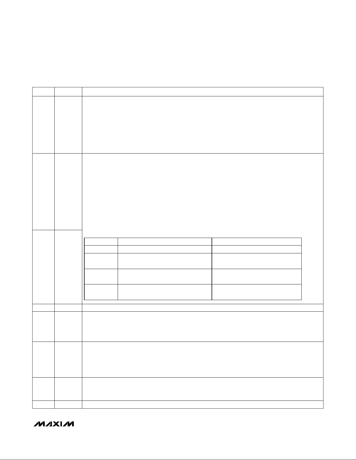
Page 1
General Description
The MAX6620 controls the speeds of up to four fans
using four independent linear voltage outputs. The
drive voltages for the fans are controlled directly over
the I
2
C interface. Each output drives the base of an
external bipolar transistor or the gate of a FET in highside drive configuration. Voltage feedback at the fan’s
power-supply terminal is used to force the correct output voltage.
The MAX6620 offers two methods for fan control. In
RPM mode, the MAX6620 monitors four fan tachometer
logic outputs for precise (±1%) control of fan RPM and
detection of fan failure. In DAC mode, each fan is driven with a voltage resolution of 9 bits and the tachometer outputs of the fans are monitored for failure.
The DAC_START input selects the fan power-supply
voltage at startup to ensure appropriate fan drive when
power is first applied. A watchdog feature turns the
fans fully on to protect the system if there are no valid
I
2
C communications within a preset timeout period.
The MAX6620 operates from a 3.0V to 5.5V power supply with low 250µA supply current, and the I
2
C-compatible interface makes it ideal for fan control in a wide
range of cooling applications. The MAX6620 is available in a 28-pin TQFN package and operates over the
-40°C to +125°C automotive temperature range.
Applications
Consumer Products
Servers
Communications Equipment
Storage Equipment
Features
♦ Controls Up to Four Independent Fans With
Linear (DC) Drive
♦ Uses Four External Low-Cost Pass Transistors
♦ 1% Accuracy Precision RPM Control
♦ Controlled Voltage Rate-Of-Change for Best
Acoustics
♦ I
2
C Bus Interface
♦ 3.0V to 5.5V Supply Voltage Range
♦ 250µA (typ) Operating Supply Current
♦ 3µA (typ) Shutdown Supply Current
♦ Small 5mm x 5mm Footprint
MAX6620
Quad Linear Fan-Speed Controller
________________________________________________________________
Maxim Integrated Products
1
×
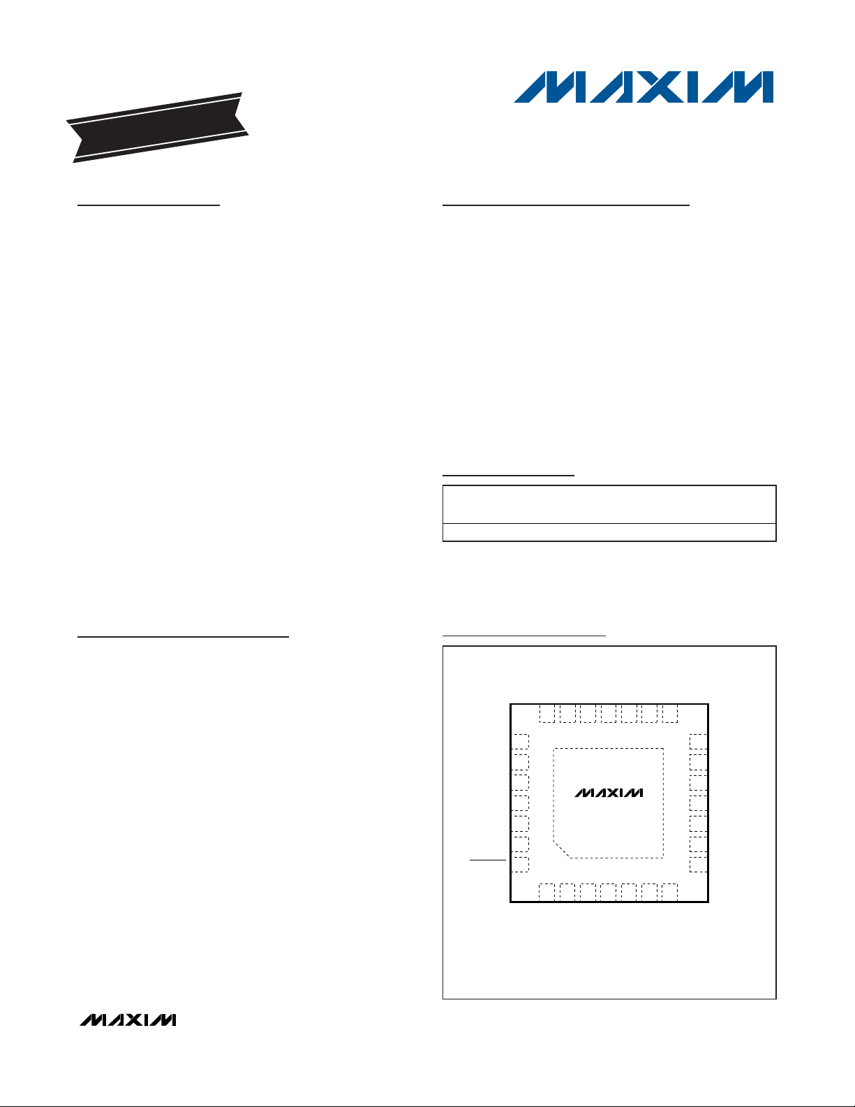
Pin Configuration
Ordering Information
19-4039; Rev 0; 3/08
For pricing, delivery, and ordering information, please contact Maxim Direct at 1-888-629-4642,
or visit Maxim’s website at www.maxim-ic.com.
EVALUATION KIT
AVAILABLE
+
Denotes a lead-free package.
*
EP = Exposed paddle.
PART
PINPACKAGE
PKG
CODE
MAX6620ATI+
T2855-8
Typical Application Circuit appears at end of data sheet.
TEMP RANGE
-40°C to +125°C 28 TQFN-EP*
TOP VIEW
TACH1
DACFB1
DACOUT1
GND
FAN
VCC
FAN_FAIL
22
23
24
25
26
27
28
DACFB2
TACH2
2021 19 17 16 15
+
12
SCL
(5mm
GND
DACOUT2
18
MAX6620
4567
3
SDA
GND
WD_START
THIN QFN
5mm × 0.8mm)
DACOUT3
DACFB3
ADDR
DAC_START
TACH3
14
TACH4
DACFB4
13
12
DACOUT4
GND
11
10
GND
X2
9
8
X1
SPINUP_START
Page 2
MAX6620
Quad Linear Fan-Speed Controller
2 _______________________________________________________________________________________
ABSOLUTE MAXIMUM RATINGS
ELECTRICAL CHARACTERISTICS
(TA= -40°C to +125°C, VCC= 3.0V to 5.5V, unless otherwise noted. Typical values are at TA= +25°C, VCC= 3.3V.) (Note 3)
Stresses beyond those listed under “Absolute Maximum Ratings” may cause permanent damage to the device. These are stress ratings only, and functional
operation of the device at these or any other conditions beyond those indicated in the operational sections of the specifications is not implied. Exposure to
absolute maximum rating conditions for extended periods may affect device reliability.
VCC to GND ..........................................................-0.3V to +6.0V
FAN_FAIL, SDA, SCL to GND ...............................-0.3V to +6.0V
ADDR, SPINUP_START, DAC_START, WD_START,
X1, X2 to GND ........................................-0.3V to (V
CC
+ 0.3V)
All Other Pins to GND..........................................-0.3V to +13.5V
Input Current at DACOUT_ Pins (Note 1) ...............+5mA/-50mA
Input Current at Any Pin (Note 1)..........................................5mA
ESD Protection (all pins, Human Body Model) (Note 2) ...±2000V
Continuous Power Dissipation (T
A
= +70°C)
28-Pin TQFN (derate 34.5mW/°C above +70°C) ....2758.6mW
Operating Temperature Range .........................-40°C to +125°C
Junction Temperature......................................................+150°C
Storage Temperature Range .............................-65°C to +150°C
Lead Temperature (soldering, 10s) .................................+300°C
Note 1: Absolute Maximum Ratings indicate limits beyond which damage to the device may occur. DC and AC electrical specifica-
tions do not apply when operating the device beyond its rated operating conditions.
Note 2: Human Body Model, 100pF discharged through a 1.5kΩ resistor.
PARAMETER SYMBOL CONDITION MIN TYP MAX UNITS
Operating Supply Voltage V
Operating Supply Current I
Quiescent Supply Current
V
Supply Voltage
FAN
DACOUT_ Output Current I
DACOUT_ Output Voltage V
DAC Feedback Voltage at Half
Scale
DAC Feedback Voltage at Full
Scale
Drive Voltage Resolution 9 Bit
DACFB_ Impedance R
TACH Minimum Input Pulse Width 25 µs
Internal Reference Frequency
Accuracy
TACH Count Accuracy (Note 4)
CC
CC
VCC = 5.5V 0.25 0.60 mA
I2C inactive 0.2 0.5 mA
Shutdown mode 3 20 µA
V
FANHI
V
FANLO
V
GND
V
DACOUT_
DACOUT_IDACOUT_
V
V
FAN
GND
FAN
At DACFB_,
FBHS
FBFS
code = 0x100,
I
DACOUT_
At DACFB_,
DAC
DAC
code = 0x1FF,
I
V
DACFB511
DACFB
DACOUT_
(Note 4) -3 +3 %
Using 32.768kHz crystal -0.1 +0.1
Using on-chip oscillator -2 +2
+ 10V < V
DACOUT_
< 11.5V,
= 12V
+ 3V < V
DACOUT_
< 10V,
= 12V
= 5mA 0.05
V
= V
FAN
FANHI
V
= V
FAN
FANLO
V
= 12V 5.54 5.74 5.94
= 5mA
= 5mA
FAN
V
= 5V 2.05 2.25 2.45
FAN
V
= V
FAN
FANHI
V
= V
FAN
FANLO
V
= 12V 11.25 11.45 11.65
FAN
= 5V 4.3 4.5 4.7
V
FAN
3.0 5.5 V
10 12 13.5
4.0 5.0 5.5
-18
-16
V
-
FAN
0.1
256/535
256/567
511/535
511/567
1MΩ
V
mA
V
V
V
%
Page 3

MAX6620
Quad Linear Fan-Speed Controller
_______________________________________________________________________________________ 3
ELECTRICAL CHARACTERISTICS (continued)
(TA= -40°C to +125°C, VCC= 3.0V to 5.5V, unless otherwise noted. Typical values are at TA= +25°C, VCC= 3.3V.) (Note 3)
PARAMETER SYMBOL CONDITION MIN TYP MAX UNITS
Fan Control Accuracy (Note 4)
Using 32.768kHz crystal, test at 850RPM -1 +1
Using on-chip oscillator -3 +3
%
XTAL Oscillator Startup Time 2s
X1 Input Threshold 0.7 V
POR Threshold
V
V
CC
FAN
2
3.5
V
LOGIC (SDA, SCL, FAN_FAIL, WD_START, TACH_)
Input High Voltage V
Input Low Voltage V
Input High Current I
Input Low Current I
IH
IL
IH
IL
VCC x
0.7
VCC x
0.3
1.0 µA
-1.0 µA
V
V
Input Capacitance All digital inputs 6 pF
Output High Current 100 µA
Output Low Voltage IOL = 3mA 0.4 V
LOGIC (DAC_START, SPIN_START, ADDR)
V
-
Input High Voltage V
Input Low Voltage V
Input High Current I
Input Low Current I
IH
IL
IH
IL
CC
0.5
V
0.5 V
1.0 µA
-1.0 µA
Input Capacitance All digital inputs 6 pF
I2C-COMPATIBLE TIMING (Notes 5, 6)
Serial Clock Frequency f
Bus Free Time Between STOP
and START Conditions
START Condition Hold Time t
STOP Condition Setup Time t
Clock Low Period t
Clock High Period t
START Condition Setup Time t
Data Setup Time t
Data Out Hold Time t
Data In Hold Time t
Maximum Receive SCL/SDA Rise
Time
Minimum Receive SCL/SDA Rise
Time
SCL
t
BUF
HD:STA
SU:STO
LOW
HIGH
SU:STA
SU:DAT
DH
HD:DAT
t
R
t
R
1.3 µs
0.6 µs
600 ns
1.3 µs
0.6 µs
600 ns
100 ns
100 ns
(Note 6) 0 0.9 µs
(Note 8) 300 ns
(Note 7)
20 + 0.1
x C
B
400 kHz
ns
Page 4
MAX6620
Quad Linear Fan-Speed Controller
4 _______________________________________________________________________________________
ELECTRICAL CHARACTERISTICS (continued)
(TA= -40°C to +125°C, VCC= 3.0V to 5.5V, unless otherwise noted. Typical values are at TA= +25°C, VCC= 3.3V.) (Note 3)
Note 3: All parts will operate properly over the VCCsupply voltage range of 3.0V to 5.5V.
Note 4: Guaranteed by design and characterization.
Note 5: All timing specifications are guaranteed by design.
Note 6: A master device must provide a hold time of at least 300ns for the SDA signal to bridge the undefined region of SCL’s falling edge.
Note 7: C
B
= total capacitance of one bus line in pF. Tested with CB= 400pF.
Note 8: Input filters on SDA and SCL suppress noise spikes less than 50ns.
Note 9: Holding the SDA line low for a time greater than t
TIMEOUT
will cause the devices to reset SDA to the idle state of the serial
bus communication (SDA set high).
t
HD,STA
t
HIGH
t
R
t
F
t
HD,STA
S Sr A
SCL
SDA
t
SU,STA
t
SU,STO
t
R
t
F
t
BUF
t
LOW
t
SU,DAT
t
HD,DAT
PS
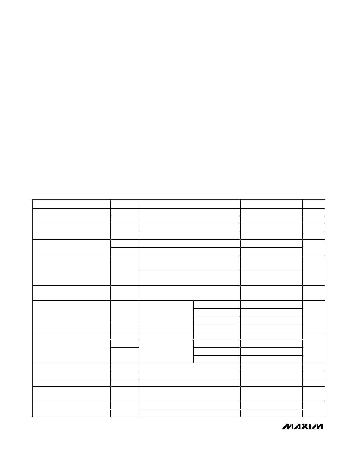
Figure 1. I2C Serial Interface Timing
PARAMETER SYMBOL CONDITION MIN TYP MAX UNITS
Maximum Receive SCL/SDA Fall
Time
Minimum Receive SCL/SDA Fall
Time
Transmit SDA Fall Time t
Pulse Width of Suppressed Spike t
Output Fall Time CL = 400pF, I
SDA Time Low for Reset of Serial
Interface
t
F
t
F
F
SP
t
TIMEOUT
(Note 7)
(Note 7)
20 + 0.1
x C
(Note 8) 0 50 ns
= 3mA 250 ns
OUT
(Note 9) 20 50 ms
300 ns
20 + 0.1
x C
B
B
250 ns
ns
Page 5
MAX6620
Quad Linear Fan-Speed Controller
_______________________________________________________________________________________ 5
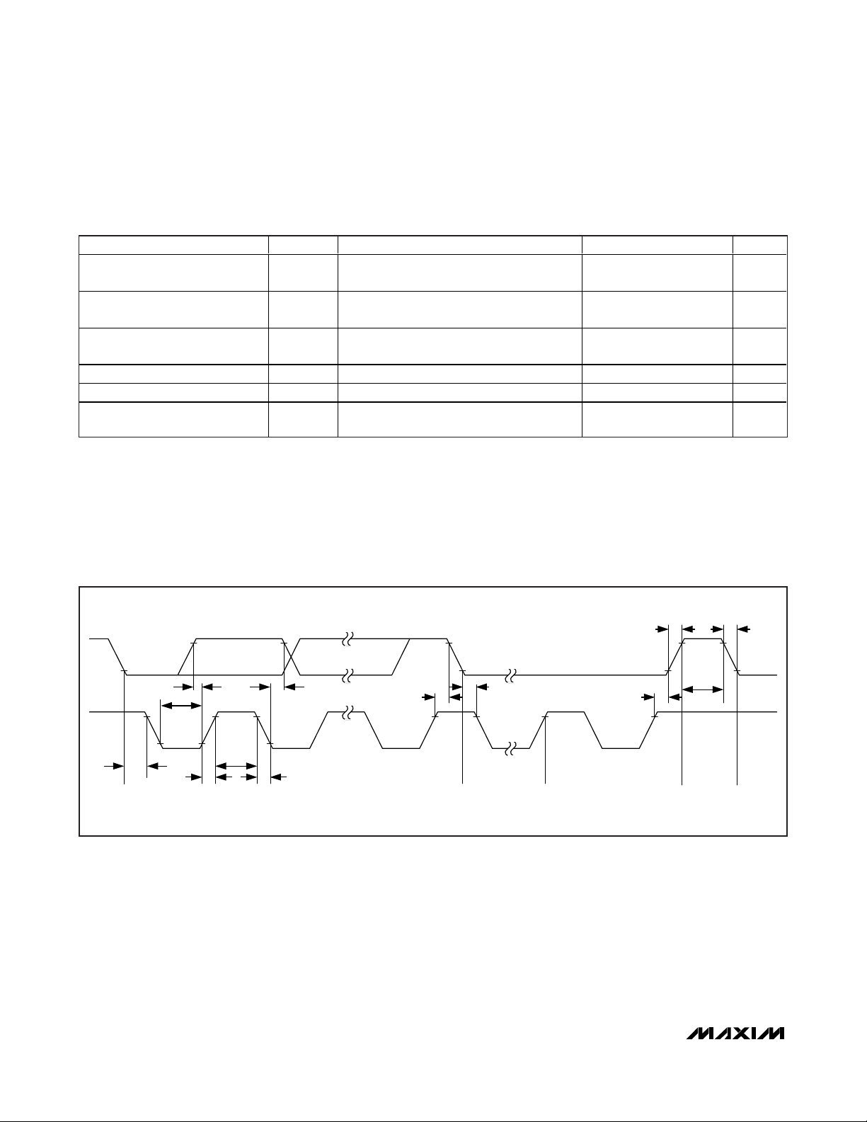
Typical Operating Characteristics
(VCC= 3.3V, V
FAN
= 12V, TA= +25°C, unless otherwise noted.)
TACH COUNT ACCURACY WITH INT CLK
vs. SUPPLY VOLTAGE
2.0
V
= 12V
FAN
1.5
1.0
0.5
TA = +25°C
0
-0.5
-1.0
-1.5
TACH COUNT ACCURACY WITH INT CLK (%)
-2.0
3.0 5.5
TA = 0°C
TA = +125°C
SUPPLY VOLTAGE (V)
TACH COUNT ACCURACY WITH EXT CLK
vs. TEMPERATURE
2.0
V
= 12V
FAN
1.5
1.0
0.5
0
-0.5
-1.0
-1.5
TACH COUNT ACCURACY WITH EXT CLK (%)
-2.0
-55 125
VCC = 3.3V, 5.0V
TEMPERATURE (°C)
TA = +70°C
TACH COUNT ACCURACY WITH EXT CLK
vs. SUPPLY VOLTAGE
2.0
V
= 12V
FAN
1.5
MAX6620 toc01
1.0
0.5
0
-0.5
-1.0
-1.5
TACH COUNT ACCURACY WITH EXT CLK (%)
-2.0
5.04.53.5 4.0
3.0 5.5
TA = 0°C, +70°C, +125°C
TA = +25°C
5.04.53.5 4.0
SUPPLY VOLTAGE (V)
MAX6620 toc02
DACFB_ VOLTAGE ACCURACY
vs. TEMPERATURE
2.0
V
= 12V
FAN
1.5
MAX6620 toc04
1.0
0.5
0
-0.5
-1.0
DACFB VOLTAGE ACCURACY (%)
-1.5
-2.0
8035-10
-55 125
VCC = 3.0V, 3.3V, 5.0V
TEMPERATURE (°C)
MAX6620 toc05
8035-10
TACH COUNT ACCURACY WITH INT CLK
vs. TEMPERATURE
2.0
V
= 12V
FAN
1.5
1.0
0.5
0
-0.5
-1.0
-1.5
TACH COUNT ACCURACY WITH INT CLK (%)
-2.0
-55 125
VCC = 5.0V
VCC = 3.3V
TEMPERATURE (°C)
DACFB_ VOLTAGE ACCURACY
vs. SUPPLY VOLTAGE
2.0
V
= 12V
FAN
1.5
1.0
0.5
0
-0.5
-1.0
DACFB VOLTAGE ACCURACY (%)
-1.5
-2.0
3.0 5.5
SUPPLY VOLTAGE (V)
MAX6620 toc03
8035-10
MAX6620 toc06
5.04.54.03.5
DACFB_ VOLTAGE ACCURACY
vs. OUTPUT CURRENT
2.0
V
= 12V
FAN
1.5
1.0
0.5
0
-0.5
-1.0
DACFB VOLTAGE ACCURACY (%)
-1.5
-2.0
5.0 10.08.57.56.55.5 9.5
VCC = 3.0V, 3.3V
VCC = 5.5V
OUTPUT CURRENT (mA)
STANDBY SUPPLY CURRENT
vs. SUPPLY VOLTAGE
500
V
= 12V
FAN
450
MAX6620 toc07
400
350
300
250
200
150
100
STANDBY SUPPLY CURRENT (μA)
50
0
9.08.07.06.0
3.0 5.5
INT CLK
EXT CLK
5.04.54.03.5
SUPPLY VOLTAGE (V)
MAX6620 toc08
OPERATING SUPPLY CURRENT (mA)
OPERATING SUPPLY CURRENT
vs. SUPPLY VOLTAGE
0.6
V
= 12V
FAN
0.5
0.4
0.3
0.2
0.1
0
3.0 5.5
INT CLK
EXT CLK
5.04.54.03.5
SUPPLY VOLTAGE (V)
MAX6620 toc09
Page 6
MAX6620
Quad Linear Fan-Speed Controller
6 _______________________________________________________________________________________
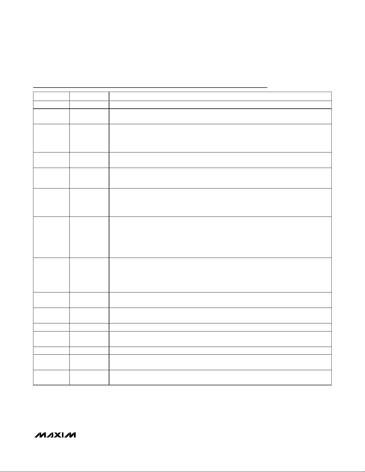
Typical Operating Characteristics (continued)
(VCC= 3.3V, V
FAN
= 12V, TA= +25°C, unless otherwise noted.)
TACH COUNT ACCURACY WITH INT CLK
vs. SUPPLY VOLTAGE
2.0
V
= 5.0V
FAN
1.5
1.0
0.5
0
-0.5
-1.0
-1.5
TACH COUNT ACCURACY WITH INT CLK (%)
-2.0
3.0 5.5
TA = +25°C
TA = +125°C
SUPPLY VOLTAGE (V)
TACH COUNT ACCURACY WITH EXT CLK
vs. TEMPERATURE
2.0
V
= 5.0V
FAN
1.5
1.0
0.5
0
-0.5
-1.0
-1.5
TACH COUNT ACCURACY WITH EXT CLK (%)
-2.0
-55 125
VCC = 3.3V, 5.0V
TEMPERATURE (°C)
TA = 0°C
TA = +70°C
TACH COUNT ACCURACY WITH EXT CLK
vs. SUPPLY VOLTAGE
2.0
V
= 5.0V
FAN
1.5
MAX6620 toc10
1.0
0.5
0
-0.5
-1.0
-1.5
TACH COUNT ACCURACY WITH EXT CLK (%)
5.04.54.03.5
-2.0
TA = 0°C, +70°C, +125°C
TA = +25°C
3.0 5.5
SUPPLY VOLTAGE (V)
5.04.54.03.5
MAX6620 toc11
DACFB_ VOLTAGE ACCURACY
vs. TEMPERATURE
4.5
V
= 5.0V
FAN
3.5
MAX6620 toc13
2.5
1.5
0.5
-0.5
-1.5
-2.5
DACFB VOLTAGE ACCURACY (%)
-3.5
8035-10
-4.5
VCC = 3.0V
VCC = 3.3V
-55 125
TEMPERATURE (°C)
VCC = 5.5V
8035-10
MAX6620 toc14
TACH COUNT ACCURACY WITH INT CLK
vs. TEMPERATURE
2.0
V
= 5.0V
FAN
1.5
1.0
0.5
0
-0.5
-1.0
-1.5
TACH COUNT ACCURACY WITH INT CLK (%)
-2.0
-55 125
VCC = 3.3V
VCC = 5.0V
TEMPERATURE (°C)
DACFB_ VOLTAGE ACCURACY
vs. SUPPLY VOLTAGE
4.5
V
= 5.0V
FAN
3.5
2.5
1.5
0.5
-0.5
-1.5
-2.5
DACFB VOLTAGE ACCURACY (%)
-3.5
-4.5
3.0 5.5
SUPPLY VOLTAGE (V)
MAX6620 toc12
8035-10
MAX6620 toc15
5.04.54.03.5
DACFB_ VOLTAGE ACCURACY
vs. OUTPUT CURRENT
4.5
V
= 5.0V
FAN
3.5
2.5
1.5
0.5
-0.5
-1.5
-2.5
DACFB VOLTAGE ACCURACY (%)
-3.5
-4.5
5.0 10.08.57.56.55.5 9.5
VCC = 3.0V, 3.3V
VCC = 5.5V
OUTPUT CURRENT (mA)
STANDBY SUPPLY CURRENT
vs. SUPPLY VOLTAGE
500
V
= 5.0V
FAN
450
MAX6620 toc16
400
350
300
250
200
150
100
STANDBY SUPPLY CURRENT (μA)
50
0
9.08.07.06.0
3.0 5.5
INT CLK
EXT CLK
5.04.54.03.5
SUPPLY VOLTAGE (V)
MAX6620 toc17
OPERATING SUPPLY CURRENT (mA)
OPERATING SUPPLY CURRENT
vs. SUPPLY VOLTAGE
0.6
V
= 5.0V
FAN
0.5
0.4
0.3
0.2
0.1
0
3.0
SUPPLY VOLTAGE (V)
MAX6620 toc18
INT CLK
EXT CLK
5.0 5.54.54.03.5
Page 7
MAX6620
Quad Linear Fan-Speed Controller
_______________________________________________________________________________________ 7
Pin Description
PIN NAME FUNCTION
1 SCL I2C Serial-Clock Input. Can be pulled up to 5.5V regardless of VCC. Open circuit when VCC = 0V.
2 SDA
3 WD_START
4, 10, 11, 18,
25
5 ADDR
6 DAC_START
7S P IN U P _S TART
8, 9 X1, X2
12, 17, 19, 24
13, 16, 20, 23
14, 15, 21, 22 TACH4–TACH1 Fan Tachometer Logic Inputs. These inputs accept input voltages up to V
26 FAN
27 VCC Power-Supply Input. 3.3V nominal. Bypass VCC to GND with a 0.1µF capacitor.
28 FAN_FAIL
—EP
GND Ground
DACOUT4–
DACOUT1
DACFB4–
DACFB1
Open-Drain, I
circuit when V
Startup Watchdog Set Input. This input is sampled when power is first applied and sets the initial
2
C watchdog behavior. When connected to GND, the watchdog function is disabled. When
I
connected to V
fan drive goes to 100%.
2
C Address Set Input. This input is sampled when power is first applied and sets the I2C slave
I
address. When connected to GND, the slave address will be 0x50. When unconnected, the slave
address will be 0x52. When connected to V
Startup Fan Drive DAC Set Input. This input is sampled when power is first applied and sets the
power-up value for the fan drive voltage. When connected to GND, the fan drive voltage will be
0%. When unconnected, the fan drive voltage will be 75%. When connected to V
voltage will be 100%.
Startup Spin-Up Set Input. This input is sampled when power is first applied and sets the initial
spin-up behavior. When connected to GND, spin-up is disabled. When connected to V
power-up, the fan is driven with a full-scale drive voltage until two tachometer pulses have been
detected, or 1s has elapsed. When unconnected, the fan is driven with a full-scale drive voltage
until two tachometer pulses have been detected, or 0.5s has elapsed. Spin-up behavior may be
modified by writing appropriate settings to the MAX6620’s registers.
Crystal Oscillator Inputs. Connections for a standard 32.768kHz quartz crystal. The internal
oscillator circuitry is designed for operation with a crystal having a specified load capacitance
(CL) of 12pF. Connect an external 32.768kHz oscillator across X1 and X2 for operation with the
external oscillator. If no crystal or external oscillator is connected, the MAX6620 will use its
internal oscillator.
Fan Drive DAC Outputs. Connect to the gate of a p-channel MOSFET or base of a PNP bipolar
transistor.
D AC Feed b ack Inp uts. C onnect a 0.1µF cap aci tor b etw een these p i ns and GN D . C onnect to the
sup p l y p i n of the fan and to the d r ai n of a p - channel M O S FE T or col l ector of a P N P b i p ol ar tr ansi stor .
Fan Power-Supply Voltage Input. Connect to the fan power supply (V
capacitor to GND.
Active-Low, Open-Drain Fan Failure Output. Active only when fault is present; open-circuit when
= 0V. This pin can be pulled up to 5.5V regardless of VCC.
V
CC
Exposed Paddle. Internally connected to GND. Connect to a large ground plane to maximize
thermal performance. Not intended as an electrical connection point.
2
C Serial-Data Input/Output. Can be pulled up to 5.5V regardless of VCC. Open
= 0V.
CC
, the MAX6620 monitors SDA. If 10s elapse without a valid I2C transaction, the
CC
, the slave address will be 0x54.
CC
CC
.
FAN
). Bypass with a 0.1µF
FAN
, the fan drive
at
CC
Page 8
MAX6620
Quad Linear Fan-Speed Controller
8 _______________________________________________________________________________________
Write Byte Format
Read Byte Format
Send Byte Format
Receive Byte Format
Slave Address: equivalent to chip-select line of
a 3-wire interface
Command Byte: selects which
register you are writing to
Data Byte: data goes into the register
set by the command byte (to set
thresholds, configuration masks, and
sampling rate)
Slave Address: equivalent to chip-select line
Command Byte: selects
which register you are
reading from
Slave Address: repeated
due to change in dataflow direction
Data Byte: reads from
the register set by the
command byte
Command Byte: sends command with no data, usually
used for one-shot command
Data Byte: reads data from
the register commanded
by the last read byte or
write byte transmission;
also used for SMBus alert
response return address
S = START CONDITION SHADED = SLAVE TRANSMISSION
P = STOP CONDITION A = NOT ACKNOWLEDGED
Figure 2. I2C Protocols
S ADDRESS RD A DATA
A
P
7 bits 8 bits
WRS A COMMAND A P
8 bits
ADDRESS
7 bits
P
1
ADATA
8 bits
ACOMMAND
8 bits
AWRADDRESS
7 bits
S
S ADDRESS WR A COMMAND A S ADDRESS
7 bits8 bits7 bits
RD A DATA
8 bits
A
P
Detailed Description
The MAX6620 controls the speeds of up to four fans
using four independent linear voltage outputs. The
drive voltages for the fans are controlled directly over
the I
2
C interface. Each of the outputs (DACOUT1–
DACOUT4) drive the base of an external PNP or the
gate of a p-channel MOSFET. Voltage feedback at the
fan’s power-supply terminal is used to force the output
voltage.
The MAX6620 monitors fan tachometer logic outputs for
precise (1%) control of fan RPM and detection of fan
failure. When the MAX6620 is used with 2-wire fans,
these inputs are not used, and the fans can be driven
to the desired voltage without using tachometer feedback.
Three inputs set the fan drive status on application of
power. The DAC_START input selects the fan-supply
voltage (100%, 75%, or 0%) at startup to ensure appropriate fan drive when power is first applied. The
SPIN_START input selects whether spin-up will be
applied to the fans at power-up. WD_START selects
whether lack of I
2
C activity will force the fans to full
speed. When the watchdog function is enabled, the
fans will be driven to full speed if there is no I2C activity
for a period of 2s, 6s, or 10s.
Digital Interface
The MAX6620 features an I2C-compatible, 2-wire serial
interface consisting of a bidirectional serial data line
(SDA) and a serial clock line (SCL). SDA and SCL facilitate bidirectional communication between the MAX6620
and the master at rates up to 400kHz. The master (typically a microcontroller) initiates data transfer on the bus
and generates SCL. SDA and SCL require 4.7kΩ (typ)
pullup resistors.
Bit Transfer
One data bit is transferred during each SCL clock
cycle. Nine clock cycles are required to transfer the
data into or out of the MAX6620. The data on SDA must
remain stable during the high period of the SCL clock
pulse, as changes in SDA while SCL is high are control
signals (see the
START and STOP Conditions
section).
Both SDA and SCL idle high.
Page 9
MAX6620
Quad Linear Fan-Speed Controller
_______________________________________________________________________________________ 9
START and STOP Conditions
The master initiates a transmission with a START condition (S), a high-to-low transition on SDA with SCL high.
The master terminates a transmission with a STOP condition (P), a low-to-high transition on SDA while SCL is high
(Figure 3). The STOP condition frees the bus and places
all devices in F/S mode (Figure 1). Use a repeated
START condition (Sr) in place of a STOP condition to
leave the bus active and in its current timing mode.
Acknowledge Bits
Successful data transfers are acknowledged with an
acknowledge bit (A) or a not-acknowledge bit (A). Both
the master and the MAX6620 (slave) generate acknowl-
edge bits. To generate an acknowledge, the receiving
device must pull SDA low before the rising edge of the
acknowledge-related clock pulse (9th pulse), and keep it
low during the high period of the clock pulse (Figure 4).
To generate a not acknowledge, the receiver allows
SDA to be pulled high before the rising edge of the
acknowledge-related clock pulse, and leaves it high
during the high period of the clock pulse. Monitoring
the acknowledge bits allows for detection of unsuccessful data transfers. An unsuccessful data transfer
happens if a receiving device is busy or if a system
fault has occurred. In the event of an unsuccessful data
transfer, the master should reattempt communication at
a later time.
A = START CONDITION
B = MSB OF ADDRESS CLOCKED INTO SLAVE
C = LSB OF ADDRESS CLOCKED INTO SLAVE
D = R/W BIT CLOCKED INTO SLAVE
E = SLAVE PULLS SMBDATA LINE LOW
F = ACKNOWLEDGE BIT CLOCKED INTO MASTER
G = MSB OF DATA CLOCKED INTO SLAVE
H = LSB OF DATA CLOCKED INTO SLAVE
I = MASTER PULLS DATA LINE LOW
J = ACKNOWLEDGE CLOCKED INTO SLAVE
K = ACKNOWLEDGE CLOCK PULSE
L = STOP CONDITION
M = NEW START CONDITION
SCL
AB CDEFG HIJ
K
SDA
t
SU:STA
t
HD:STA
t
LOWtHIGH
t
SU:DAT
t
HD:DAT
t
SU:STO
t
BUF
L
M
Figure 3. I2C Write Timing Diagram
A = START CONDITION
B = MSB OF ADDRESS CLOCKED INTO SLAVE
C = LSB OF ADDRESS CLOCKED INTO SLAVE
D = R/W BIT CLOCKED INTO SLAVE
E = SLAVE PULLS SMBDATA LINE LOW
F = ACKNOWLEDGE BIT CLOCKED INTO MASTER
G = MSB OF DATA CLOCKED INTO MASTER
H = LSB OF DATA CLOCKED INTO MASTER
I = MASTER PULLS DATA LINE LOW
J = ACKNOWLEDGE CLOCKED INTO SLAVE
K = ACKNOWLEDGE CLOCK PULSE
L = STOP CONDITION
M = NEW START CONDITION
SCL
AB CDEFG
HIJ
SDA
t
SU:STAtHD:STA
t
LOW
t
HIGH
t
SU:DAT
t
SU:STOtBUF
LMK
Figure 4. I2C Read Timing Diagram
Page 10

MAX6620
Slave Address
A master initiates communication with a slave device by
issuing a START condition followed by a slave address
byte. As shown in Figure 5, the slave address byte consists of 7 address bits and a read/write bit (R/W). When
idle, the MAX6620 continuously waits for a START condition followed by its slave address. The first four bits
(MSBs) of the slave address have been factory programmed and are always 0101 and the seventh bit is 0.
Connect ADDR to GND or V
CC
, or leave it unconnected
to program D2 and D1 of the slave address according
to Table 1.
After receiving the address, the MAX6620 (slave)
issues an acknowledgement by pulling SDA low for one
clock cycle.
Data Byte (Read and Write)
Single Read and Burst Read. A single read begins
with the bus master issuing a START condition followed
by the seven slave ID address bits and a zero (WR,
Figure 2), which is followed by an acknowledge bit (A)
from the slave corresponding to the slave ID. Next, the
master sends out an 8-bit register address, which is
also followed by an acknowledge bit from the slave.
The bus master issues another START condition and
the same seven slave ID address bits followed by a one
(RD, Figure 2), with the slave producing an acknowledge bit. The slave then sends out the 8-bit data corresponding to the register address previously written by
the master. The bus master sends back a not-acknowledge bit (A). This completes the single read process
and a STOP condition is issued by the bus master.
In a burst read, the process is the same as a single
read except that the bus master issues an acknowledge bit after each byte transmitted by the slave. After
each acknowledge bit, the register address increments
by one, and the data from the next register is transmitted by the slave. The process continues, with data
reads followed by acknowledges. After the register with
the highest address is read, the register pointer rolls
over to point to the first register. To terminate a burst
read, the bus master issues a STOP condition.
Single Write and Burst Write. A single write begins
with the bus master issuing a START condition followed
by the seven slave ID address bits and a zero (WR,
Figure 2), which is followed by an acknowledge bit (A)
from the slave corresponding to the slave ID. Next, the
master sends out an 8-bit register address, which is
also followed by an acknowledge bit from the slave.
After the acknowledge bit, 8-bit data is written to the
register, and the slave issues a third acknowledgement.
A STOP condition is issued by the bus master to complete the single write process.
In a burst write, the process is similar to a single write
except that the master does not issue a STOP condition
immediately after the first byte has been written. After
the first write is completed, the slave issues an
acknowledge bit, the register address increments by
one, and the data to be written to the next register is
transmitted by the master. The process continues, with
data writes followed by acknowledges. After the register with the highest available address is written, the register pointer rolls over to point to the first register. To
terminate a burst write, the bus master issues a STOP
condition.
Fan Drive
The MAX6620 uses external pass transistors to power
the fans. DACOUT1–DACOUT4 adjust the powersupply voltage for each fan by driving the base of a
PNP bipolar transistor, or the gate of a p-MOSFET. The
resulting fan-supply voltage is fed back to DACFB_.
This closes the voltage feedback loop. The system
power supply for the output devices is V
FAN
. V
FAN
is
Quad Linear Fan-Speed Controller
10 ______________________________________________________________________________________
Table 1. Slave Address Setting with
ADDR Pin
SDA
SCL
0101
1234
D2 D1 0 R/W
56789
S
A
ACKNOWLEDGE
Figure 5. MAX6620 Slave Address Byte
ADDR CONNECTION
GND 0x50 0101 000
Unconnected 0x52 0101 010
V
CC
SLAVE ADDRESS
HEX BINARY
0x54 0101 100
Page 11

MAX6620
Quad Linear Fan-Speed Controller
______________________________________________________________________________________ 11
Figure 6. Read and Write Summary
P
AM
AS
8-BIT DATA
BIT 7…….…………BIT 0 ACK BIT
8-BIT DATA8-BIT REGISTER ADDRESS
BIT 7…….…….…………BIT 0 ACK BIT
1ASS P
BIT 7………….…………BIT 0 ACK BITBIT 7…………….……………BIT 0 ACK BIT
BIT 7……….…………………BIT 0 ACK BIT
LAST 8-BIT DATA AS PS
BIT 7…………….…………BIT 0 ACK BIT
AS7-BIT SLAVE ID 0 AS
AM
LAST 8-BIT DATA
BIT 7……….……………BIT 0 ACK BIT
FIRST 8-BIT DATA
AS
8-BIT REGISTER ADDRESS
8-BIT REGISTER ADDRESS
BIT 7…………….………BIT 0 ACK BIT BIT 7…………….……………BIT 0 ACK BIT
0 AS AS S 7-BIT SLAVE ID
7-BIT SLAVE ID 0 AS ASS P
BIT 7…………….……………… BIT 0 ACK BIT BIT 7…………….…………………BIT ACK BIT
7-BIT SLAVE ID
SINGLE WRITE
BIT 7…………….……….BIT 0 ACK BIT
SINGLE READ
BURST WRITE
BIT 7…………….…………BIT 0 ACK BIT
S
8-BIT REGISTER ADDRESS
BIT 7…………….…………… BIT 0 ACK BIT
0 AS AS 7-BIT SLAVE ID 1 AS FIRST 8-BIT DATA AM
7-BIT SLAVE ID
BIT 7…………….………… BIT 0 ACK BIT
BURST READ
S
S: 2-WIRE BUS START CONDITION BY MASTER
P: 2-WIRE BUS STOP CONDITION BY MASTER
AS: ACKNOWLEDGE BY SLAVE
AM: ACKNOWLEDGE BY MASTER
AM: NO ACKNOWLEDGE BY MASTER
Page 12

MAX6620
nominally 12V or 5V. The drive to the fans is proportional to V
FAN
. See the
Fan_ Target Drive Voltage Registers
and the
Applications Information
sections for more
details.
Fan-Speed Control
DAC (Voltage) Mode. In DAC mode, the MAX6620 sim-
ply sets the voltage that powers the fan. The fan’s
speed is related, but not precisely proportional to, the
drive voltage. The drive voltage is set by the Fan_
Target Drive Voltage registers and may be read from
the Fan_ Drive Voltage registers. Because the output
voltage can ramp to new values at a controlled rate, the
values in the two registers may be different. See the
Register Descriptions
and
Applications Information
sec-
tions for details.
RPM Mode. In RPM mode, the MAX6620 monitors
tachometer output pulses from the fan and adjusts the
fan drive voltage to force the fan’s speed to the desired
value. Fan speed is measured by counting the number
of internal 8192Hz clock cycles that take place during a
selectable number of tachometer periods. The number
of clock cycles counted (11-bit value) is stored in the
Fan_ TACH Count registers, and the desired number of
cycles is stored in the Fan_ Target TACH Count registers. See the
Register Descriptions
and
Applications
Information
sections for details.
Rate-of-Change Control. Sudden changes in fan
speed can be easily heard by users. The MAX6620
helps reduce the audibility of fan-speed changes by
controlling the rate at which the drive to the fan is incremented. Four bits in the Fan_ Dynamics registers set
the rate at which the fan drive voltage is incremented.
This allows the time required for a change in fan speed
to be varied from 0 (in DAC mode only) to several minutes. See the
Register Descriptions
and
Applications
Information
sections for details.
Monitoring Tachometer Signals. The TACH_ inputs
accept tachometer or “locked-rotor” output signals from
3- or 4-wire fans. When measuring fan speed, the
MAX6620 counts the number of internal 8192Hz clock
cycles that occur during 1, 2, 4, 8, 16, or 32 tachometer
periods. The number of tachometer periods is selectable for each fan by using the appropriate Fan_
Dynamics register. Tachometer pulses <25µs in duration are ignored to minimize the effect of noise on the
tachometer lines.
The TACH count for a given RPM can be obtained from
the following equation:
where:
NP = number of tachometer pulses per revolution. Most
general-purpose brushless DC fans produce two
tachometer pulses per revolution.
SR = 1, 2, 4, 8, 16, or 32. See the Fan_ Speed Range
information in the
Fan_ Dynamics Registers(06h, 07h,
08h, 09h)—POR = 0100 1100
section.
The tachometer count consists of 11 bits in the Fan_
TACH Count registers and is available in RPM and DAC
modes. In RPM mode, the desired fan count is written
to the Fan_ Target TACH Count registers.
Fan Failure Detection
When enabled, the MAX6620 monitors the TACH_
inputs to determine when a fan has failed. For fans with
tachometer outputs, failure is detected in various ways
depending on the fan control mode. In every case, four
consecutive fault detections are required to decide
whether the fan has failed. In DAC mode, the Fan_
Target TACH Count registers hold the upper limit for
tachometer count values; a fault condition is identified
when a TACH count exceeds the value written to the
Fan_ Target TACH Count registers for more than 1s. In
RPM mode, a fault condition is identified when any of
the following three conditions occur for more than 1s: 1)
the TACH count exceeds the value of the Fan_ Target
TACH Count registers while the fan drive voltage is at
full-scale, 2) the TACH count exceeds two times the
Fan_ Target TACH Count value, or 3) the TACH count
reaches its full count of 7FF.
Some fans have locked rotor outputs that produce a
logic-level output to indicate that the fan has stopped
spinning. These signals can be monitored by setting
D2:D1 in the Fan_ Configuration registers. D2 selects
locked rotor or tachometer monitoring and D1 selects the
polarity of the locked rotor signal. A fan fault has occurred
when a locked rotor signal has been present for 1s.
Fan failure is indicated in the Fan Fault register and
also with the open-drain FAN_FAIL output. The
FAN_FAIL output may be masked using the mask bits
in the Fan Fault register. When a fan failure is detected,
drive to the affected fan is removed. Drive may be
restored by writing a new DAC or fan count target to the
fan’s control registers. The global configuration regis-
Quad Linear Fan-Speed Controller
12 ______________________________________________________________________________________
SR
TACH count
=
60
NP
×
SR
×× =
RPM
8192
491520
×
NP RPM
×
Page 13

ter’s bit D4 can be used to cause a fan failure to force
the remaining fan speeds to 100%.
Watchdog
The MAX6620 includes an optional I2C watchdog function that monitors the I2C bus for transactions. When the
watchdog function is enabled, all fans will be forced to
full speed if no I2C transactions occur within a selected
period (2s, 6s, or 10s).
Spin-Up
When a fan is not spinning, and a voltage less than the
nominal fan-supply voltage is applied to its powersupply terminals, it may fail to start spinning. To overcome this, the full nominal supply voltage may be
applied to the fan terminals for a short time before a
lower voltage is applied. This “spin-up” period allows
the fan to overcome inertia and begin operating. Spinup is controlled using the Fan_ Configuration registers.
Spin-up can be disabled, or it can cause the fan to be
driven with the full supply voltage until it produces two
tachometer pulses, up to a maximum of 0.5s, 1s, or 2s
when the fan is started.
POR Options
Three inputs allow set up of the MAX6620’s behavior at
power-up. These inputs are sampled when power is
first applied to the MAX6620:
• WD_START. Connect WD_START to VCCto enable,
or to ground to disable, the watchdog function. When
enabled using WD_START, the timeout period is 10s.
After power is applied, the watchdog function may be
enabled or disabled through the global configuration
register.
• SPINUP_START. At power-up, spin-up operation is
controlled by the SPINUP_START pin, which can be
connected to ground (spin-up disabled), VCC(spinup for a maximum of 1s), or unconnected (spin-up for
a maximum of 0.5s).
• DAC_START. This input controls the fan drive volt-
age (for all four fans) at power-up. When connected
to ground, the initial fan drive voltage will be 0V.
When connected to V
CC
, the initial fan drive voltage
will be full scale. When unconnected, the initial fan
drive voltage will be 75% of V
FAN
.
MAX6620
Quad Linear Fan-Speed Controller
______________________________________________________________________________________ 13
Page 14

MAX6620
Quad Linear Fan-Speed Controller
14 ______________________________________________________________________________________
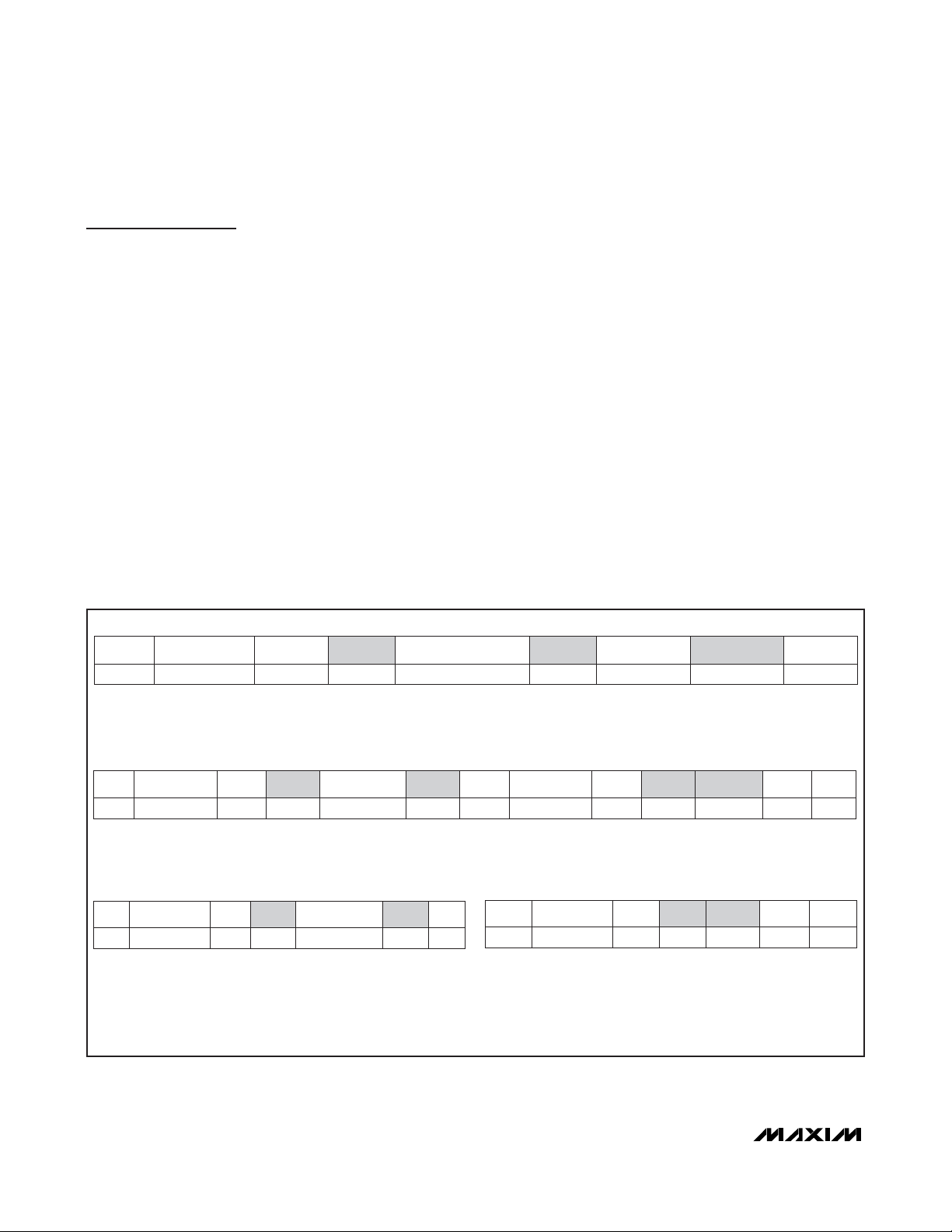
Register Map
Registers
C
2
I
1 =
S tatus
Watchd og
el ap sed
( r ead onl y) :
Rotor
0 = l ow
Locked
P ol ar i ty:
1 = hi g h
01 = 2s
10 = 6s
00 = N o w atchd og
OS C :
0 = i nter nal
failure:
100% on
(35ms):
Timeout
P OR:
0 = nor m al
Run:
0 = r un
11 = 10s
r otor
Rotor :
TAC H /
Locked
0 = TAC H
1 = l ocked
i np ut
TAC H
00 = N o sp i n- up
01 = tw o TAC H counts
M od e:
or 0.5s
0 = D AC
enab l e
or 1s
10 = tw o TAC H counts
1 = RP M
11 = tw o TAC H counts
or 2s
111 = 1s p er LS B
110 = 0.5s p er LS B
101 = 0.25s p er LS B
D AC Rate- of- C hang e:
0.0625s p er LS B ( RP M m od e)
000 = 0s p er LS B ( D AC m od e)
S am e as Fan 1 C onfi g ur ati on
S am e as Fan 1 C onfi g ur ati on
S am e as Fan 1 C onfi g ur ati on
000 = 1
001 = 2
S p eed Rang e ( TAC H p er i od s) :
100 = 0.125s p er LS B
011 = 0.0625s p er LS B
010 = 0.03125s p er LS B
001 = 0.015625s p er LS B
S am e as Fan 1 D ynam i cs
S am e as Fan 1 D ynam i cs
S am e as Fan 1 D ynam i cs
010 = 4
011 = 8
100 = 16
101 = 32
110 = 32
111 = 32
1 = X TAL
0 = enabled
1 = disabled
0 = enabled
1 = disabled
S p i n- U p :
1 = r eset
1 = standby
C W atchd og :
2
I
Fans to
Bus
F U N C T IO N D 7 D 6 D 5 D 4 D 3 D 2 D 1 D 0
PO R
ST A T E
R EGIST ER
N O ./A D DR ESS
R /W
Gl ob al
C onfi g ur ati on
R/W 00h 0000 0X X X
R/W 01h 0000 1111 Fan Faul t Fan 4 Faul t Fan 3 Faul t Fan 2 Faul t Fan 1 Faul t Fan 4 Mask Fan 3 Mask Fan 2 Mask Fan 1 Mask
Fan 1
C onfi g ur ati on
R/W 02h 0X X 0 0000
Fan 2
C onfi g ur ati on
R/W 03h 0X X 0 0000
Fan 3
C onfi g ur ati on
R/W 04h 0X X 0 0000
Fan 4
R/W 05h 0X X 0 0000
Fan 1
C onfi g ur ati on
D ynam i cs
R/W 06h 0100 1100
Fan 2
D ynam i cs
R/W 07h 0100 1100
Fan 3
D ynam i cs
R/W 08h 0100 1100
Fan 4
D ynam i cs
R/W 09h 0100 1100
Page 15

MAX6620
Quad Linear Fan-Speed Controller
______________________________________________________________________________________ 15
X = Depends on input states at power-up.
Register Map (continued)
S am e as Fan 1 TAC H C ount
S am e as Fan 1 TAC H C ount
S am e as Fan 1 TAC H C ount
S am e as Fan 1 D r i ve V ol tag e
S am e as Fan 1 D r i ve V ol tag e
S am e as Fan 1 D r i ve V ol tag e
S am e as Fan 1 Tar g et TAC H C ount
S am e as Fan 1 Tar g et TAC H C ount
S am e as Fan 1 Tar g et TAC H C ount
S am e as Fan 1 Tar g et D r i ve V ol tag e
S am e as Fan 1 Tar g et D r i ve V ol tag e
S am e as Fan 1 Tar g et D r i ve V ol tag e
D 2D 1D 0—————
C ount
C ount
13h 1110 0000
R
C ount
Fan 3 TAC H
15h 1110 0000
14h 1111 1111
R
Fan 4 TAC H
16h 1111 1111
F U N C T IO N D 7 D 6 D 5 D 4 D 3 D 2 D 1 D 0
Fan 1 TAC H
Fan 2 TAC H
PO R
ST A T E
11h 1110 0000
10h 1111 1111 D 10 D 9D 8D 7D 6D 5D 4D 3
12h 1111 1111
R EG IST ER
N O . /A D D R ESS
R
R /W
C ount
17h 1110 0000
R
D 0——————Ful l
V ol tag e
V ol tag e
1Bh 0000 0000
R
V ol tag e
Fan 3 D r i ve
1C h 0000 0000
1D h 0000 0000
R
Fan 4 D r i ve
1E h 0000 0000
R
Fan 1 D r i ve
Fan 2 D r i ve
19h 0000 0000
18h 0000 0000 D 8D 7D 6D 5D 4D 3D 2D 1
1Ah 0000 0000
R
D 2D 1D 0—————
V ol tag e
Fan 1 Tar g et
TAC H C ount
Fan 2 Tar g et
TAC H C ount
1Fh 0000 0000
21h 0000 0000
20h 0011 1100 D 10 D 9D 8D 7D 6D 5D 4D 3
R/W
23h 0000 0000
22h 0011 1100
R/W
Fan 3 Tar g et
TAC H C ount
25h 0000 0000
24h 0011 1100
R/W
Fan 4 Tar g et
TAC H C ount
27h 0000 0000
26h 0011 1100
R/W
D 0———————
Fan 1 Tar g et
Fan 2 Tar g et
2Ah X X X X X X X X
D r i ve V ol tag e
2Bh X 000 0000
R/W
2C hX X X X X X X X
Fan 3 Tar g et
R/W
D r i ve V ol tag e
2D hX 000 0000
28h X X X X X X X X D 8D 7D 6D 5D 4D 3D 2D 1
D r i ve V ol tag e
29h X 000 0000
R/W
Fan 4 Tar g et
2E hX X X X X X X X
R/W
D r i ve V ol tag e
2Fh X 000 0000
Page 16

MAX6620
Quad Linear Fan-Speed Controller
16 ______________________________________________________________________________________
Global Configuration Register (00h)—POR = 0000 0XXX
Register Descriptions
BIT R/W FUNCTION
Run:
7 R/W
0 = run
1 = standby
6 R/W
5 R/W
4 R/W
3 R/W
POR:
0 = norma l operation
1 = reset all registers to POR values
Thi s bit automatically re sets itself and will always return a 0 when read.
2
C Bus Timeout:
I
0 = enabled
1 = disabled
2
C interface will reset if SDA is low for more than 35ms.
The I
Fans to 100% on failure:
0 = if a fan fai lure is detected, all other fan channels immediately go to full-scale drive vo ltage to
ensure adequate coo ling
1 = disabled
Oscillator Selection:
Selects on-chip oscillator or 32.768kHz crystal/ceramic resonator. Use crystal if 1% RPM accuracy is
required.
0 = internal oscillator (default at power-on)
1 = external 32.768kHz crystal
When switching from the internal osci llator to an external crystal, the MAX6620 operates from the internal
oscillator until the crystal oscillator has started up. If the crystal is damaged or the oscillator fails to start,
the MAX6620 will continue to operate from the internal oscillator.
Page 17

MAX6620
Quad Linear Fan-Speed Controller
______________________________________________________________________________________ 17
Global Configuration Register (00h)—POR = 0000 0XXX (continued)
BIT R/W FUNCTION
I
When active, the watchdog monitors SDA and SCL for va lid I
transactions between the ma ster and the MAX6620 within the watchdog period, all fan output vo ltages
2
R/W
1
0 R
will go to full-scale drive voltage.
If the watchdog times out and va lid I
previous DAC va lue. The master can then program the output vo ltages, target TACH counts, or other
functions in the normal manner.
When the w atchdog function is active, ensure that the master communicates to the MAX6620
periodically, for example reading a status register.
The POR state is set by the state of the WD_START pin at power-up.
I
This bit is cleared by I
2
C Watchdog:
2
C transactions begin to occur again, operation will resume with the
D2:D1 I
00 Inactive (no watchdog) WD_START = GND
01 2 —
10 6 —
11 10 WD_START = V
2
C Watchdog Status:
2
0 = I
C transactions occurred within watchdog period
1 = time between I
2
C WATCHDOG PERIOD (s) POR CONDITION
2
C transact ion exceeds watchdog period
2
C read from this register.
2
C transactions . If there are no va lid
CC
Page 18

MAX6620
Quad Linear Fan-Speed Controller
18 ______________________________________________________________________________________
Fan Fault Register (01h)—POR = 0000 1111
BIT R/W FUNCTION
7 R
6 R Fan 3 Fault Status
5 R Fan 2 Fault Status
4 R Fan 1 Fault Status
3 R/W
2 R/W Fan 3 Fault Mask
1 R/W Fan 2 Fault Mask
0 R/W Fan 1 Fault Mask
Fan 4 Fault Status:
Indicates which fans have had faults detected. When a fan fault is detected, the drive to the fan is disabled and
the corresponding fault bit is set. The fault bits latch until they are cleared by reading, thus allowing short-term
faults to be identified. After a fault status bit is cleared by reading, the corresponding output voltage will
remain zero until a Fan_ Target Drive Voltage register or Fan_ Target TACH Register is written. Writing a
new target drive voltage or target TACH count will cause drive to be applied to the fan again, at which time a
new failure-detection cycle will begin.
Fault Conditions Are:
MODE
DAC Any
RPM
FAN_FAIL will be asserted when four consecutive faults are detected.
Fan 4 Fault Mask:
Masks faults on selected fans from asserting the FAN_FAIL output. Faults will still be indicated by the fault
status bits:
0 = not masked
1 = masked
FAN_ DRIVE
VOLTAGE REGISTER
1FF (full)
<1FF
CONDITION
TACH count exceeds value of Fan_ Target
TACH count
Locked rotor asserts
TACH count exceeds value of Fan_ Target
TACH Count
TACH count exceeds two times of Fan_ Target
TACH Count value
TACH count reaches it full count of 7FF
TIME
(s)
>1
>1
Page 19
MAX6620
Quad Linear Fan-Speed Controller
______________________________________________________________________________________ 19
Fan_ Configuration Registers (02h, 03h, 04h, 05h)—POR = 0XX0 0000
BIT R/W FUNCTION
RPM/DAC:
0 = DAC mode. The fan drive voltage is set by the value in the Fan_ Target Drive Voltage register.
1 = RPM mode. The fan drive voltage is adjusted to produce the TACH count value in the Fan_ Target
7 R/W
6 R/W
5 R/W
TACH Count regi ster.
When chang ing from DAC to RPM mode, if the current RPM value is different from the value selected in
the Fan_ Target TACH Count register, the drive voltage will start from the current va lue and increment/
decrement toward the desired value at the se lected DAC rate-of-change.
Spin-Up:
When the fan drive voltage increa se s from 0V to a value less than the ful l-s cale drive vo ltage, it may be
necess ary to drive the fan with the full-sca le drive voltage for a brief period to ensure that the fan is
spinning before reducing the drive to the selected va lue.
When spin-up is selected, the fan i s driven at the full-scale drive vo ltage until two tachometer pulses
have been detected or loc ked rotor has been cleared. A maxi mum spin-up time is a lso selectable to
ensure that the spin-up time is not excess i ve. After two tachometer pulses have been detected, or locked
rotor has been cleared or the spin-up has timed out, the drive voltage goes to the value in the Fan_ Target
Drive Voltage register.
The POR state is set by the state of the SPINUP_START pin at power-up.
D6:D5 FUNCTION POR CONDITION
00 No spin-up SPIN_START pin = ground
01
10
11
Spin-up until two tachometer pul se s or
clearing of locked rotor, or 0.5s (ma x)
Spin-up until two tachometer pul se s or
clearing of locked rotor, or 1s (max)
Spin-up until two tachometer pul se s or
clearing of locked rotor, or 2s (max)
SPIN_START pin = open
SPIN_START pin = V
—
CC
4 Reserved
TACH Input Enable:
3 R/W
2 R/W
1 R/W
0 — Reserved
Enables TACH input function and fan fault detection (automatically enabled in RPM mode).
0 = disabled. When disabled and TACH input is not used, bit 1 and bit 2 are ignored.
1 = enabled
TACH/Locked Rotor:
Selects TACH input function as TACH count or locked rotor. In locked rotor mode, the TACH count stops
and assertion of the TACH input indicates that the fan ha s stopped.
0 = TACH count
1 = locked rotor
Locked Rotor Polarity:
0 = low locked rotor. TACH input low in locked rotor mode indicates fan is stopped.
1 = high locked rotor. TACH input high in locked rotor mode indicates fan is stopped.
Page 20

MAX6620
Quad Linear Fan-Speed Controller
20 ______________________________________________________________________________________
Fan_ Dynamics Registers (06h, 07h, 08h, 09h)—POR = 0100 1100
BIT R/W FUNCTION
7 R/W
6 R/W
5 R/W
Fan_ Speed Range:
The MAX6620 determines fan speed by counting the number of internal 8192Hz clock cycles (using an 11bit counter) during one or more fan tachometer periods. Three bits set the nominal RPM range for the fan, as
shown in the table below. As an example, a setting of 010 causes the MAX6620 to count the number of
8192Hz clock cycles that occur during four complete tachometer periods. If the fan has a nominal speed of
2000RPM and two tachometer pulses per revolution, one tachometer period will be nominally 15ms, and four
tachometer periods will be 60ms. With an 8192Hz clock, the TACH count will therefore be equal to 491. With
a fan speed of 1/3 the nominal value, the count will be 1474. If the fan’s nominal speed is 1000RPM, the fullspeed TACH count will be 983. At 1/3 the nominal speed, there will be 2948 clock cycles in four tachometer
periods. This is greater than the maximum 11-bit count of 2047, so four tachometer periods is too many for
this fan; a setting of 001 (two clock cycles) is recommended instead.
The table below shows the full-speed tachometer counts for several combinations of nominal fan speeds
and D7:D5 settings. The shaded combinations will provide the best results. When setting D7:D5, the goal is
to obtain the highest tachometer count without exceeding the maximum count of 2047 when the fan is at the
minimum speed of interest. For example, if the minimum speed of interest is 1/3 of full speed, the maximum
tachometer count will be three times the value shown in the table below:
Tachometer Counts/(Counting Period) (8192Hz Clock Used):
NUMBER OF
D7:D5
TACH PERIODS
COUNTED
000 1
001 2
010 4
011 8
100 18
101,
110,
111
32
500 1000 2000 4000 8000 16000
491
(60ms)
983
(120ms)
1966
(240ms)
2047
(480ms)
2047
(960ms)
2047
(1920ms)
245
(30ms)
491
(60ms)
983
(120ms)
1966
(240ms)
2047
(480ms)
2047
(960ms)
(120ms)
(240ms)
(480ms)
RPM
122
(15ms) 61(7.5ms) 30(3.75ms) 15(1.875ms)
245
(30ms)
491
(60ms)
983
1966
2047
122
(15ms) 61(7.5ms) 30(3.75ms)
245
(30ms)
491
(60ms)
983
(120ms
1966
(240ms)
122
(15ms) 61(7.5ms
245
(30ms)
491
(60ms)
983
(120ms)
122
(15ms)
245
(30ms
491
(60ms)
Page 21

MAX6620
Quad Linear Fan-Speed Controller
______________________________________________________________________________________ 21
Fan_ Dynamics Registers (06h, 07h, 08h, 09h)—POR = 0100 1100 (continued)
BIT R/W FUNCTION
Fan_ DAC Rate-of-Change:
The fan drive voltage (at the DACFB_ inputs) varies from 0 to full scale in 512 increments. The rate-ofchange bits determine the time interval between output voltage increments/decrements. In RPM mode, a
setting of 0 would result in an unstable feedback loop, so a default value of 0.0625 is in effect when 0 is
selected.
4 R/W
3 R/W
2 R/W
Regardless of the settings, there are a few cases for which the rate-of-change is always 0:
•
When a target TACH count of 2047 (7FF) is selected, the fan drive voltage immediately goes to 0V. A
full-scale target count is assumed to mean that the intent is to shut down the fan, and going directly to 0
drive avoids the possibility of loss of control-loop feedback at high TACH counts. If a slow- speed
decrease toward 0 is desired, a target TACH count at the slowest practical value for the fan should be
chosen. Once that count has been reached, selecting a count of 2047 (7FF) will then take the drive
immediately to 0V.
• When a target fan drive voltage of 0V is selected, the drive voltage immediately goes to 0V. Again, it is
assumed that the intent is to shut down the fan. If a slow-speed decrease toward 0 is desired, a target
fan drive voltage of the slowest practical value for the fan in question should be chosen. Once that drive
voltage has been reached, selecting a target value of 0 will then take the drive immediately to 0V.
• When the current drive level is 0 in DAC mode, selecting a new target fan drive voltage will immediately
take the voltage to that value. The fan will spin-up first if spin-up is enabled.
• When the current drive level is 0 in RPM mode, selecting a new target TACH count that is less than 2047
(7FF) will immediately take the drive voltage to the value in the Fan_ Target Drive Voltage register. From
this value, the drive voltage will increment as needed to achieve the desired TACH count. The fan will
spin-up first if spin-up is enabled.
TIME BETWEEN OUTPUT VOLTAGE
D4:D2
DAC MODE RPM MODE
000 0 0.0625 0
001 0.015625 10
010 0.03125 20
011 0.0625 (default) 40
100 0.125 80
101 0.25 160
110 0.5 320
111 1.0 640
INCREMENTS (s)
TIME FROM 33%
TO 100%
(s)
1 — Reserved
0 — Reserved
Page 22
MAX6620
Quad Linear Fan-Speed Controller
22 ______________________________________________________________________________________
Fan_ TACH Count Registers (10h, 12h, 14h, 16h)—POR = 1111 1111
Fan_ TACH Count Registers (11h, 13h, 15h, 17h)—POR = 1110 0000
Fan_ Drive Voltage Registers (18h, 1Ah, 1Ch, 1Eh)—POR = 0000 0000
Fan_ Drive Voltage Registers (19h, 1Bh, 1Dh, 1Fh)—POR = 0000 0000
BIT R/W FUNCTION
7
6
5
4
3
2
1
0
BIT R/W FUNCTION
7
6
5
BIT R/W FUNCTION
7
6
5
4
3
2
1
0
R
R Fan_ TACH Count D7:D5
R
Fan_ TACH Count D10:D3:
Indicates the number of 8192Hz clock pulses counted during the counting period. The Fan_ TACH Count
consists of 11 bits contained in two bytes.
To minimize noise from spurious tachometer transitions, pulses less than 25µs are ignored.
Fan_ Drive Voltage D8:D1:
This is a 9-bit value that ranges from 0 to 511.
This register shows the actual fan drive voltage. When the value in this register is 480V, the nominal fan drive
voltage of V
is supplied to the fan, as shown in the table in the Fan_ Target Drive Voltage Registers section.
FAN
BIT R/W FUNCTION
7RFan_ Drive Voltage D0
Full-Scale Status:
0R
0 = DAC is driving with value of D8:D0 that is not at full scale
1 = DAC is driving with full scale voltage
Page 23
MAX6620
Quad Linear Fan-Speed Controller
______________________________________________________________________________________ 23
Fan_ Target TACH Count Registers (21h, 23h, 25h, 27h)—POR = 0000 0000
Fan_ Target TACH Count Registers (20h, 22h, 24h, 26h)—POR = 0011 1100
The Fan_ Target TACH Count consists of 11 bits contained in two bytes. The two bytes must be written in
order in one or two I
2
C transactions, with no other I2C
writes in between. These target registers are updated
internally at the same time when a second byte (LSB) is
written.
BIT R/W FUNCTION
7
6
5
4
R/W
3
2
1
0
Fan_ Target TACH Count D10:D3:
In RPM mode, write the desired tachometer count to this register. The MAX6620 will then adjust the fan drive
voltage to achieve this tachometer count.
In DAC mode, this register has no effect.
When changing from DAC mode to RPM mode, best results are obtained by loading this register with the
desired TACH count before changing to RPM mode. The target TACH count for a given RPM will be obtained
by the following equation:
TargetTACH
where:
NP = number of TACH pulses per revolution
SR = 1, 2, 4, 8, 16, or 32 (see the fan_ speed range information in the Fan_ Dynamics Registers (06h, 07h, 08h,
09h)—POR = 0100 1100 section)
=
NP
BIT R/W FUNCTION
7
6
5
R Fan_ Target TACH Count D2:D0
×
××608192
RPM
SR
Page 24
MAX6620
Quad Linear Fan-Speed Controller
24 ______________________________________________________________________________________
The Fan_ Target Drive Voltage consists of 9 bits contained in two bytes. The two bytes must be written in
order in one or two I
2
C transactions with no other I2C
writes in between. These target registers are updated
internally at the same time when a second byte (LSB) is
written.
Fan_ Target Drive Voltage Registers (29h, 2Bh, 2Dh, 2Fh)—POR = X000 0000
Fan_ Target Drive Voltage Registers (28h, 2Ah, 2Ch, 2Eh)—POR = XXXX XXXX
BIT R/W FUNCTION
7
6
5
4
R/W
3
2
Fan_ Target Drive Voltage D8:D1:
This is a 9-bit value that ranges from 0 to 511 and is contained in two bytes. In DAC mode, write the
desired fan drive voltage to these two registers. The MAX6620 will then ramp the fan drive voltage to
this va lue at a rate determined by the DAC rate-of-change bit s.
In RPM mode, the value contained in this register will be the vo ltage applied to the fan immed iately after
spin-up or after changing the Fan_ Target TACH Count from 2047 (7FF) to a value lower than 2047 (7FF).
For example, if the fan is currently stopped with spin-up disab led, and a new Fan_ Target TACH Count
corresponding to 60% of the full-sca le fan speed is to be selected, the fan voltage can be programmed
to immediately go to 60% of the full-scale drive voltage when the new Fan_ Target TACH Count is
selected from 2047 (7FF), and then clo se the RPM control loop starting from that voltage.
The register value is converted to the drive vo ltage at the fan (or voltage at DACFB _) as fol lows:
D8:D0 FAN_ DRIVE VOLTAGE (V)
DECIMAL HEX 5V RANGE 12V RANGE
0 000h 0.000 0.000
200 0C8h 1.764 4.486
300 12Ch 2.646 6.729
400 190h 3.527 8.972
480 1E0h 4.232 10.766
511 1FFh 4.506 11.462
The value of the Fan_ Target Drive Voltage at POR depends on state of the DAC_START pin, as show n
1
0
below:
D8:D0
DECIMAL HEX
0 000h GND
384 180h Open
511 1FF VCC
DAC_START
Bit R/W FUNCTION
7RFan_ Target Drive Voltage D0
Page 25

MAX6620
Quad Linear Fan-Speed Controller
______________________________________________________________________________________ 25
Applications Information
External Pass Transistors
Match external pass transistors to the fans being used.
Ensure that the pass transistor is capable of handling
the maximum fan current. For best results, the pass
transistor’s maximum current rating should be at least
50% greater than the fan’s nominal supply current.
The transistor should also be capable of dissipating the
worst-case power, which usually occurs when the fan is
being driven to approximately 50% of the nominal supply voltage. The maximum power dissipation will
depend on the thermal resistance of the transistor, its
case, and the printed-circuit board (PCB) to which it is
soldered. For example, if the worst-case transistor
power dissipation occurs when the fan current is
100mA, and the voltage across the fan is 6.5V, the
maximum power dissipation will be 650mW. A
BCP69T1-D in a SOT223-4 package is rated at 1.5W at
25°C (about 1W at 70°C) when soldered to a 0.93in
2
(6cm2) copper PCB pad, and can easily handle this
power dissipation. Larger copper pads, packages with
lower thermal resistance, or different transistors can
give significantly different results.
The MAX6620 uses an advanced output driver design
that eliminates the large external capacitors often connected across the fan’s power-supply terminals. For
stability with a variety of fans, connect a 0.1µF capacitor from DACFB_ to ground.
Using a Low-Dropout Voltage Regulator
(LDO) as the Pass Device
Voltage regulators can be used instead of discrete transistors to drive the fans (Figure 7). The voltage feedback loop is closed around the regulator to provide the
desired output voltage. When using a voltage regulator,
note the following:
• Most regulators require relatively large capacitors at
their inputs and outputs for stability.
• Most regulators have a lower output voltage limit that
is >0V. If removing the drive from the fan is necessary when using a regulator, choose a regulator that
has an on/off control input and drive that input from
the system microcontroller.
Fan-Speed Control (DAC and RPM Modes)
The MAX6620 has two main modes for controlling fan
speeds. In DAC mode, the MAX6620 produces an output voltage that drives the fan. This voltage is proportional to the main fan power-supply voltage (V
FAN
).
Write the 9-bit desired voltage value in the Fan_ Target
Drive Voltage register.
In RPM mode, the MAX6620 monitors the tachometer
signals from the fans through the TACH_ inputs and
adjusts the drive voltage to yield the desire tachometer
count. The tachometer count is the number of internal
8192 clock cycles that are counted during the selected
number of tachometer pulses.
Controlling 2-Wire Fans (DAC Mode)
In DAC mode, the MAX6620 sets the fan’s supply voltage to the value selected in the Fan_ Target Drive
Voltage register. Tachometer monitoring is never done
when controlling a 2-wire fan, so the TACH input enable
bit in the Fan_ Configuration register should be set to 0.
Enabling the TACH input when using a 2-wire fan will
result in an erroneous fan failure detection.
Initial Settings:
• Begin with the POR settings. The POR value of the
fan_ DAC rate-of-change bits (4:2 of the Fan_
Dynamics Register) can yield slower fan speed
changes than desired. If this is the case, choose a
faster value, such as 001.
Starting the Fan:
• Write the desired drive voltage value to the Fan_
Target Drive Voltage register.
Changing Speeds:
• Write the new desired drive voltage value to the Fan_
Target Drive Voltage register.
Stopping the Fan:
• Write a voltage value of 0 to the Fan_ Target Drive
Voltage register.
Controlling 3-Wire Fans (DAC Mode)
In DAC mode, the MAX6620 sets the fan’s supply voltage to the value selected in the Fan_ Target Drive
Voltage register. 3-wire fans with tachometer outputs
allow monitoring of the fan’s speed to detect fan failure.
To monitor a fan’s speed, the TACH input should be
enabled.
Page 26

MAX6620
Quad Linear Fan-Speed Controller
26 ______________________________________________________________________________________
Figure 7. Using Low Dropout Voltage Regulators Instead of Discrete Transistors as the Pass Devices
V
C
470Ω
DACOUT1
TO I2C MASTER
FAN_FAIL
SDA
SCL
V
CC
3.0V TO 5.5V
0.1μF
V
+12V
FAN
0.1μF
DACFB1
TACH1
DACOUT2
DACFB2
V
FAN
V
C
470Ω
V
FAN
V
FAN
+12V
V
IN
PQ20RX
V
FAN
V
IN
PQ20RX
0.33μF
V
O
V
ADJ
2.4kΩ
27kΩ
0.33μF
V
O
V
ADJ
2.4kΩ
27kΩ
47μF
FAN1
47μF
V
CC
(OPTIONAL CRYSTAL)
ADDR
DAC_START
SPINUP_START
WD_START
X1
X2
I2C INTERFACE,
REGISTERS, AND
CONTROL LOGIC
DAC OUTPUT
DRIVER
TACH MONITOR
TACH2
DACOUT3
DACFB3
TACH3
DACOUT4
DACFB4
TACH4
V
FAN
V
IN
V
470Ω
V
FAN
V
470Ω
V
FAN
V
PQ20RX
V
FAN
V
IN
PQ20RX
O
V
ADJ
2.4kΩ
27kΩ
V
O
V
ADJ
2.4kΩ
27kΩ
C
C
FAN2
0.33μF
47μF
FAN3
0.33μF
47μF
FAN3
Page 27

MAX6620
Quad Linear Fan-Speed Controller
______________________________________________________________________________________ 27
Initial Settings:
• Begin with the POR settings. The POR value of the
fan_ DAC rate-of-change bits (4:2 of the Fan_
Dynamics register) can yield slower fan speed
changes than desired. If this is the case, choose a
faster value, such as 001.
• Write the desired number of tachometer periods to
be counted in the speed range bits (7:5 of the Fan_
Dynamics register).
• Write the maximum allowable tachometer count to the
Fan_ Target TACH Count registers. Tachometer
counts greater than this value will result in a fan fault
detection. Choose a value that will not be encountered during normal operation, accounting for normal
fan speed tolerances.
Note: Setting a full-scale target count (2047) will
result in the fan drive going to 0V.
• Set the TACH input enable bit in the Fan_
Configuration register to 1.
Note: This bit can be set after the fan has been started, if desired. If the bit is set before writing a target
fan drive voltage, the target drive voltage should be
set immediately after enabling the TACH input to
avoid failure detection before the fan has started
spinning.
Starting the Fan:
• Write the desired drive voltage value to the Fan_
Target Drive Voltage register.
Changing Speeds:
• Write the new desired drive voltage value to the Fan_
Target Drive Voltage register.
Stopping the Fan:
• Write a 0 to the TACH input enable bit in the Fan_
Configuration register. This prevents the MAX6620
from deciding that the fan has failed after it has
stopped.
• Write a voltage value of 0V to the Fan_ Target Drive
Voltage register.
• If a gradual decrease in fan speed is desired, write
the lowest drive voltage at which the fan will reliably
operate. When the drive voltage reaches that value,
write 0V to the Fan_ Target Drive Voltage register.
Controlling 3-Wire Fans (RPM Mode)
Begin as in DAC mode and start the fan.
Changing from DAC Mode to RPM Mode:
• Write the desired tachometer count to the Fan_ TACH
Count registers.
• Set bit 7 of the Fan_ Configuration register to 1. This
selects RPM mode. The fan will go to the selected
speed.
Note: When the DAC rate-of-change is set to one of
the faster values, the fan drive voltage can, depending on the fan’s characteristics, undergo a slow oscillation. While this rarely has an audible impact, it can
be reduced or eliminated by selecting a slower rateof-change once the fan’s speed has reached or
approached its target value.
Changing Speeds:
• Write the desired tachometer count to the Fan_
Target TACH Count registers.
Stopping the Fan:
• Write the current drive voltage into the Fan_ Target
Drive Voltage register.
• Write a value greater than the current tachometer
count into the Fan_ Target TACH Count register.
• Write a 0 to bit 7 of the Fan_ Configuration register.
This selects DAC mode.
• Write a 0 to the TACH input enable bit in the Fan_
Configuration register. This prevents the MAX6620
from detecting a high TACH count and determining
that the fan has failed.
• Write a voltage value of 0V to the Fan_ Target Drive
Voltage register.
• If a gradual decrease in fan speed is desired, write
the lowest drive voltage at which the fan will reliably
operate. When the drive voltage reaches that value,
write 0 to the Fan_ Target Drive Voltage register.
Page 28

MAX6620
Quad Linear Fan-Speed Controller
28 ______________________________________________________________________________________
Typical Application Circuit
Chip Information
PROCESS: CMOS
TO I2C MASTER
V
CC
FAN_FAIL
SDA
SCL
ADDR
DAC_START
V
CC
0.1μF
I2C INTERFACE,
REGISTERS, AND
CONTROL LOGIC
V
FAN
0.1μF
DAC OUTPUT
DRIVER
TACH MONITOR
DACOUT1
DACFB1
TACH1
DACOUT2
DACFB2
TACH2
DACOUT3
DACFB3
TACH3
0.1μF
0.1μF
0.1μF
4.7kΩ
4.7kΩ
4.7kΩ
4.7kΩ
4.7kΩ
4.7kΩ
0.1μF
V
FAN
FAN1
0.1μF
V
FAN
FAN2
0.1μF
V
FAN
FAN3
SPINUP_START
(OPTIONAL CRYSTAL)
WD_START
DACOUT4
X1
X2
GND
DACFB4
0.1μF
TACH4
4.7kΩ
V
4.7kΩ
0.1μF
FAN
FAN4
Page 29

MAX6620
Quad Linear Fan-Speed Controller
______________________________________________________________________________________ 29
Package Information
(The package drawing(s) in this data sheet may not reflect the most current specifications. For the latest package outline information
go to www.maxim-ic.com/packages
.)
QFN THIN.EPS
Page 30

Package Information (continued)
(The package drawing(s) in this data sheet may not reflect the most current specifications. For the latest package outline information
go to www.maxim-ic.com/packages
.)
Maxim cannot assume responsibility for use of any circuitry other than circuitry entirely embodied in a Maxim product. No circuit patent licenses are
implied. Maxim reserves the right to change the circuitry and specifications without notice at any time.
30
____________________Maxim Integrated Products, 120 San Gabriel Drive, Sunnyvale, CA 94086 408-737-7600
© 2008 Maxim Integrated Products is a registered trademark of Maxim Integrated Products, Inc.
Quad Linear Fan-Speed Controller
MAX6620
 Loading...